

W3214
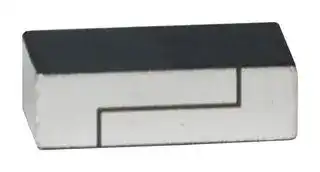
Antenna, 868 MHz, 10mm x 3.2mmx 5mm
- Manufacturer: PULSE ELECTRONICS
- Product type: Antennas - Single Band Chip
- SVHC: No SVHC (04-Feb-2026)
- Product Range: -
- Centre Frequency: 868MHz
- Antenna Case Size: 10mm x 3.2mmx 5mm
| Delivery and price | |
|---|---|
| Units per pack | 500 |
| Price | 0.992 € |
| Current stock | 500+ |
| Lead time | 30 days |
## **Series:** Chip Antenna ## **Description:** 868MHz On Ground Ceramic SMD Loop Antenna **PART NUMBER: W3214** ## **Features:** - Frequency 863-873 MHz - Size 10 x 3.2 x 5mm - Full metal under antenna - Peak Gain 1dBi - Peak Efficiency 55% - RoHs Compliant - MSL level 1 ## **Applications:** - 868MHz ISM band radios - IoT devices - Sensors, monitoring - Industry automation All dimensions are in mm / inches ## Issue: 2049 In the effort to improve our products, we reserve the right to make changes judged to be necessary. CONFIDENTIAL AND PROPRIETARY INFORMATION This document contains confidential and proprietary information of Pulse Electronics, Inc. (Pulse) and is protected by copyright, trade secret and other state and federal laws. Its receipt or possession does not convey any rights to reproduce, disclose its contents, or to manufacture, use or sell anything it may describe. Reproduction, disclosure or use without specific written authorization of Pulse is strictly forbidden. For more information: Pulse Worldwide Headquarters 15255 Innovation Drive #100 San Diego, CA 92128 USA Tel:1-858-674-8100 Pulse/Larsen Antennas Europe Headquarters 18110 SE 34[th] St Bldg 2 Suite 250 Pulse GmbH & Do, KG Vancouver, WA 98683 Zeppelinstrasse 15 USA Herrenberg, Germany Tel: 1-360-944-7551Tel: 49 7032 7806 0 Pulse (Suzhou) Wireless Products Co, Inc. 99 Huo Ju Road(#29 Bldg,4[th] Phase Suzhou New District Jiangsu Province, Suzhou 215009 PR China Tel: 86 512 6807 9998 1 ## **Series:** Chip Antenna ## **Description:** 868MHz On Ground Ceramic SMD Loop Antenna ## **PART NUMBER: W3214** Frequency 863-873MHz Nominal Impedance 50 Return Loss Peak -20dB Return Loss Band edge -5dB Radiation Pattern Omni Peak Gain 1dBi Efficiency 38% (55% peak) Polarization Linear Power Withstanding 5W **MECHANICAL SPECIFICATIONS** Overall Length 10x3.2x5mm Weight 0.73g Antenna Material Ceramic with silver plating ## **ENVIRONMENTAL SPECIFICATIONS** Operating Temperature -40~+85°C Storage Temperature -40~+85°C RoHS Compliant Yes ## Issue: 2049 In the effort to improve our products, we reserve the right to make changes judged to be necessary. CONFIDENTIAL AND PROPRIETARY INFORMATION This document contains confidential and proprietary information of Pulse Electronics, Inc. (Pulse) and is protected by copyright, trade secret and other state and federal laws. Its receipt or possession does not convey any rights to reproduce, disclose its contents, or to manufacture, use or sell anything it may describe. Reproduction, disclosure or use without specific written authorization of Pulse is strictly forbidden. 2 ## **Series:** Chip Antenna ## **Description:** 868MHz On Ground Ceramic SMD Loop Antenna ## **PART NUMBER: W3214** ## **MECHANICAL DRAWING** **==> picture [163 x 14] intentionally omitted <==** **----- Start of picture text -----**<br> 1 2<br>**----- End of picture text -----**<br> |No.|Terminal Name|Terminal Dimensions| |---|---|---| |1|Feed / GND|1.5 x 2.75 mm| |2|Feed / GND|1.5 x 2.75 mm| |Antenna is symmetrical. Either of terminals 1 or 2 can be Feed / GND||| ## Issue: 2049 In the effort to improve our products, we reserve the right to make changes judged to be necessary. CONFIDENTIAL AND PROPRIETARY INFORMATION This document contains confidential and proprietary information of Pulse Electronics, Inc. (Pulse) and is protected by copyright, trade secret and other state and federal laws. Its receipt or possession does not convey any rights to reproduce, disclose its contents, or to manufacture, use or sell anything it may describe. Reproduction, disclosure or use without specific written authorization of Pulse is strictly forbidden. 3 ## **Series:** Chip Antenna ## **Description:** 868MHz On Ground Ceramic SMD Loop Antenna ## **PART NUMBER: W3214** ## **MECHANICAL DRAWING AND TERMINAL CONFIGURATION** # _**Ground cleared under antenna TOP and MIDDLE layers, clearance area 10.8 mm x 8.25mm (BOTTOM layer solid ground)**_ ## Issue: 2049 In the effort to improve our products, we reserve the right to make changes judged to be necessary. CONFIDENTIAL AND PROPRIETARY INFORMATION This document contains confidential and proprietary information of Pulse Electronics, Inc. (Pulse) and is protected by copyright, trade secret and other state and federal laws. Its receipt or possession does not convey any rights to reproduce, disclose its contents, or to manufacture, use or sell anything it may describe. Reproduction, disclosure or use without specific written authorization of Pulse is strictly forbidden. 4 **PART NUMBER: W3214** ## **Series:** Chip Antenna ## **Description:** 868MHz On Ground Ceramic SMD Loop Antenna ## **MECHANICAL DRAWING AND TERMINAL CONFIGURATION** ## _**Recommended Antenna Pad Dimensions on PCB Layout (top surface) Ground cleared under antenna on top and inner layers, clearance area 10.8 mm x 8.25 mm**_ _**All metallization must be removed from top and inner layers, clearance Area ( 10.8 x 8.25 mm )**_ ## **Bottom solid ground layer** ## Issue: 2049 In the effort to improve our products, we reserve the right to make changes judged to be necessary. CONFIDENTIAL AND PROPRIETARY INFORMATION This document contains confidential and proprietary information of Pulse Electronics, Inc. (Pulse) and is protected by copyright, trade secret and other state and federal laws. Its receipt or possession does not convey any rights to reproduce, disclose its contents, or to manufacture, use or sell anything it may describe. Reproduction, disclosure or use without specific written authorization of Pulse is strictly forbidden. 5 ## **Series:** Chip Antenna ## **Description:** 868MHz On Ground Ceramic SMD Loop Antenna **PART NUMBER: W3214** |**MECHANICAL DRAWING AND TERMINAL CONFIGURATION**|**MECHANICAL DRAWING AND TERMINAL CONFIGURATION**|**MECHANICAL DRAWING AND TERMINAL CONFIGURATION**|**MECHANICAL DRAWING AND TERMINAL CONFIGURATION**|| |---|---|---|---|---| |_Recommended Antenna Pad Dimensions on PWB Layout (top surface)_||||| ||||1,70|| ||el<br>9,10<br>ofS<br>10,80<br>pO] oO 0 0<br>FO<br>OO|||| ||||OoD)|| |**1**<br>**2**<br>**3**<br>essen<br>ro.<br>8||||| |RAIS<br>col t}00) Oo||DETAIL|V2IRS<br> D<br>O|—|—la|+|| ||**PCB contact pads**||**PCB contact pads**|| |No.|Terminal Name||Terminal Dimensions|| |1|Feed||1.70 x 1.45 mm|| |2|GND||1.70 x 1.45 mm|| |3|GND||1.70 x 3.20 mm|| ## Issue: 2049 In the effort to improve our products, we reserve the right to make changes judged to be necessary. CONFIDENTIAL AND PROPRIETARY INFORMATION This document contains confidential and proprietary information of Pulse Electronics, Inc. (Pulse) and is protected by copyright, trade secret and other state and federal laws. Its receipt or possession does not convey any rights to reproduce, disclose its contents, or to manufacture, use or sell anything it may describe. Reproduction, disclosure or use without specific written authorization of Pulse is strictly forbidden. 6 ## **Series:** Chip Antenna ## **Description:** 868MHz On Ground Ceramic SMD Loop Antenna **PART NUMBER: W3214** ## **MECHANICAL DRAWING AND TERMINAL CONFIGURATION** ## _Recommended test board layout for electrical characteristic measurement, test board outline size 120 x 37mm_ ## Issue: 2049 In the effort to improve our products, we reserve the right to make changes judged to be necessary. CONFIDENTIAL AND PROPRIETARY INFORMATION COMPLIANT This document contains confidential and proprietary information of Pulse Electronics, Inc. (Pulse) and is protected by copyright, trade secret and other state and federal laws. Its receipt or possession does not convey any rights to reproduce, disclose its contents, or to manufacture, use or sell anything it may describe. Reproduction, disclosure or use without specific written authorization of Pulse is strictly forbidden. 7 ## **Series:** Chip Antenna ## **Description:** 868MHz On Ground Ceramic SMD Loop Antenna **PART NUMBER: W3214** ## **CHARTS** Measured on the 120x37mm test board with matching circuit, 10pF shunt capacitor, position center location of test board edge. Ground cleared under antenna, clearance area 10.80 mm x 8.25 mm top and middle layers. ## Issue: 2049 In the effort to improve our products, we reserve the right to make changes judged to be necessary. CONFIDENTIAL AND PROPRIETARY INFORMATION This document contains confidential and proprietary information of Pulse Electronics, Inc. (Pulse) and is protected by copyright, trade secret and other state and federal laws. Its receipt or possession does not convey any rights to reproduce, disclose its contents, or to manufacture, use or sell anything it may describe. Reproduction, disclosure or use without specific written authorization of Pulse is strictly forbidden. 8 ## **Series:** Chip Antenna ## **Description:** 868MHz On Ground Ceramic SMD Loop Antenna **PART NUMBER: W3214** ## **CHARTS** Measured on the 120x37mm test board with matching circuit, 10pF shunt capacitor, position center location of test board edge. Ground cleared under antenna, clearance area 10.80 mm x 8.25 mm top and middle layers. ## Issue: 2049 This document contains confidential and proprietary information of Pulse Electronics, Inc. (Pulse) and is protected by copyright, trade secret and other state and federal laws. Its receipt or possession does not convey any rights to reproduce, disclose its contents, or to manufacture, use or sell anything it may describe. Reproduction, disclosure or use without specific written authorization of Pulse is strictly forbidden. 9 In the effort to improve our products, we reserve the right to make changes judged to be necessary. CONFIDENTIAL AND PROPRIETARY INFORMATION ## **Series:** Chip Antenna ## **Description:** 868MHz On Ground Ceramic SMD Loop Antenna **PART NUMBER: W3214** ## **CHARTS** Measured on the 120x37mm test board with matching circuit, 10pF shunt capacitor, position center location of test board edge. Ground cleared under antenna, clearance area 10.80 mm x 8.25 mm top and middle layers. ## Issue: 2049 This document contains confidential and proprietary information of Pulse Electronics, Inc. (Pulse) and is protected by copyright, trade secret and other state and federal laws. Its receipt or possession does not convey any rights to reproduce, disclose its contents, or to manufacture, use or sell anything it may describe. Reproduction, disclosure or use without specific written authorization of Pulse is strictly forbidden. 10 In the effort to improve our products, we reserve the right to make changes judged to be necessary. CONFIDENTIAL AND PROPRIETARY INFORMATION ## **Series:** Chip Antenna ## **Description:** 868MHz On Ground Ceramic SMD Loop Antenna ## **PART NUMBER: W3214** ## **CHARTS** Measured on the 120x37mm test board with matching circuit, 10pF shunt capacitor, position center location of test board edge. Ground cleared under antenna, clearance area 10.80 mm x 8.25 mm top and middle layers. ## **Radiation Pattern** ## **XY Plane** **==> picture [437 x 311] intentionally omitted <==** **----- Start of picture text -----**<br> 0<br>5<br>863MHz<br>330 0 30<br>Avg(dBi) = -4.41<br>-5 Peak(dBi) = -0.81<br>-10 Avg -3(deg) = 147.5<br>-15<br>300 60 868MHz<br>-20 Avg (dBi) = -3.62<br>-25 Peak (dBi) = 0.28<br>Avg -3 (deg) = 130.5<br>-30<br>-35 873MHz<br>270 -40 90 Avg (dBi) = -5.11<br>Peak (dBi) = -1.19<br>Avg -3 (deg) = 129.5<br>240 120<br>210 150<br>180 Phi Angle (°)<br>863MHz 868MHz 873MHz<br>Power (dBm)<br>**----- End of picture text -----**<br> ## Issue: 2049 In the effort to improve our products, we reserve the right to make changes judged to be necessary. CONFIDENTIAL AND PROPRIETARY INFORMATION This document contains confidential and proprietary information of Pulse Electronics, Inc. (Pulse) and is protected by copyright, trade secret and other state and federal laws. Its receipt or possession does not convey any rights to reproduce, disclose its contents, or to manufacture, use or sell anything it may describe. Reproduction, disclosure or use without specific written authorization of Pulse is strictly forbidden. 11 ## **Series:** Chip Antenna ## **Description:** ‘ec 868MHz On Ground Ceramic SMD Loop Antenna ## **PART NUMBER: W3214** ## **CHARTS** Measured on the 120x37mm test board with matching circuit, 10pF shunt capacitor, position center location of test board edge. Ground cleared under antenna, clearance area 10.80 mm x 8.25 mm top and middle layers. ## **Radiation Pattern** **==> picture [443 x 333] intentionally omitted <==** **----- Start of picture text -----**<br> ZX Plane<br>0<br>5<br>863MHz<br>330 30<br>0<br>Avg(dBi) = -4.48<br>-5 Peak(dBi) = -0.09<br>Avg -3(deg) = 90.5<br>-10<br>300 60 868MHz<br>-15<br>Avg (dBi) = -3.83<br>-20<br>Peak (dBi) = 0.78<br>-25 Avg -3 (deg) = 85.5<br>(= -30 873MHz<br>270 -35 90 Avg (dBi) = -5.24<br>Peak (dBi) = -1.03<br>Avg -3 (deg) = 96.5<br>240 120<br>\am/<br>CT<br>210 150<br>180 Phi Angle (°)<br>863MHz 868MHz 873MHz<br>Power (dBm)<br>**----- End of picture text -----**<br> ## Issue: 2049 In the effort to improve our products, we reserve the right to make changes judged to be necessary. CONFIDENTIAL AND PROPRIETARY INFORMATION This document contains confidential and proprietary information of Pulse Electronics, Inc. (Pulse) and is protected by copyright, trade secret and other state and federal laws. Its receipt or possession does not convey any rights to reproduce, disclose its contents, or to manufacture, use or sell anything it may describe. Reproduction, disclosure or use without specific written authorization of Pulse is strictly forbidden. 12 ## **Series:** Chip Antenna ## **Description:** 868MHz On Ground Ceramic SMD Loop Antenna ## **PART NUMBER: W3214** ## **CHARTS** Measured on the 120x37mm test board with matching circuit, 10pF shunt capacitor, position center location of test board edge. Ground cleared under antenna, clearance area 10.80 mm x 8.25 mm top and middle layers. ## **Radiation Pattern** ## **YZ Plane** **==> picture [444 x 317] intentionally omitted <==** **----- Start of picture text -----**<br> 0<br>10<br>863MHz<br>330 5 30<br>Avg(dBi) = -4.48<br>0 Peak(dBi) = -0.09<br>-5 Avg -3(deg) = 90.5<br>-10<br>300 60 868MHz<br>-15 Avg (dBi) = -3.83<br>-20 Peak (dBi) = 0.78<br>Avg -3 (deg) = 85.5<br>-25<br>-30 873MHz<br>270 -35 90 Avg (dBi) = -5.24<br>/ Peak (dBi) = -1.03<br>Avg -3 (deg) = 96.5<br>240 120<br>210 150<br>180 Phi Angle (°)<br>863MHz 868MHz 873MHz<br>Power (dBm)<br>**----- End of picture text -----**<br> ## Issue: 2049 In the effort to improve our products, we reserve the right to make changes judged to be necessary. CONFIDENTIAL AND PROPRIETARY INFORMATION This document contains confidential and proprietary information of Pulse Electronics, Inc. (Pulse) and is protected by copyright, trade secret and other state and federal laws. Its receipt or possession does not convey any rights to reproduce, disclose its contents, or to manufacture, use or sell anything it may describe. Reproduction, disclosure or use without specific written authorization of Pulse is strictly forbidden. 13 ## **Series:** Chip Antenna ## **Description:** 868MHz On Ground Ceramic SMD Loop Antenna **PART NUMBER: W3214** ## **PACKAGING** ## 350pcs antennas per 7” reel 3pcs 7” reel per inner package box 2pcs inner box per out box Total 2100pcs antenna per out box Out box size: 390mmx215mmx165mm ## Label area **==> picture [14 x 7] intentionally omitted <==** **----- Start of picture text -----**<br> 350<br>**----- End of picture text -----**<br> ## Issue: 2049 This document contains confidential and proprietary information of Pulse Electronics, Inc. (Pulse) and is protected by copyright, trade secret and other state and federal laws. Its receipt or possession does not convey any rights to reproduce, disclose its contents, or to manufacture, use or sell anything it may describe. Reproduction, disclosure or use without specific written authorization of Pulse is strictly forbidden. 14 In the effort to improve our products, we reserve the right to make changes judged to be necessary. CONFIDENTIAL AND PROPRIETARY INFORMATION
Updated at April 28, 2026
Pulse Electronics, a YAGEO company, is a global leader in the design and manufacturing of passive electronic components. With a legacy of innovation dating back to 1956, the company provides essential technology for the communications, computing, industrial, transportation, and IoT sectors. Pulse is recognized worldwide for delivering high-performance solutions that power advanced applications, ranging from 5G networks and electric vehicles to data centers and smart grids. The company's extensive product portfolio is heavily anchored in power and networking magnetics. This includes a comprehensive range of power inductors engineered for exceptional efficiency and reliability in demanding environments. To address complex electromagnetic compatibility challenges, Pulse also manufactures highly effective EMC and RFI suppression solutions, such as common mode chokes and filters, alongside specialized toroidal and RF inductors designed to ensure clean power delivery and optimal signal integrity. Beyond traditional magnetics, Pulse excels in the development of advanced wireless and power conversion components. Their connectivity solutions feature a wide array of high-performance RF antennas and single-band chip antennas tailored for modern connected devices. Furthermore, to support sophisticated power architectures, Pulse provides a broad spectrum of transformers—encompassing PCB-mounted designs, current sensing transformers, and precise pulse transformers—equipping engineers with robust, industry-proven components for power isolation and measurement.
About Novapart
Novapart is a B2B electronic component broker specialising in stock shortages and cost reduction. We source hard-to-find parts and identify compliant alternatives across a catalogue of 410,000+ components from 500+ manufacturers.
Learn more →Stock Shortage Specialist
When a component is unavailable, discontinued or has an unacceptable lead time, we tap into our network of vetted European and Asian distributors to source what you need — without compromising on quality or traceability.
Request a quote →Compliant Alternatives
We identify pin-to-pin, electrically equivalent substitutes that meet the same certifications (RoHS, AEC-Q100, REACH) as your original specification — validated against datasheets, not just part numbers. Often at a lower cost.
BOM Analysis service →