


VVZ40-16IO1
Thyristor Diode Module, Bridge Rectifier, Three Phase - SCR/Diode, 0.065 A, 1 V, V1-B-Pack
- Manufacturer: LITTELFUSE
- Product type: Thyristors - SCR Modules
- SVHC: To Be Advised
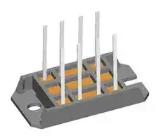
- No. of Pins: 8Pins
- Product Range: -
- SCR Module Type: Bridge Rectifier, Three Phase - SCR / Diode
- Thyristor Mounting: Panel
- On State RMS Current: 100A
- Thyristor Case Style: V1-B-Pack
- Average Forward Current: 45A
- Gate Trigger Current Max: 65mA
- Gate Trigger Voltage Max: 1V
- Operating Temperature Max: 125°C
- Repetitive Peak Reverse Voltage: 1.6kV
- Peak Repetitive Off State Voltage: 1.6kV
| Delivery and price | |
|---|---|
| Units per pack | 50 |
| Price | 29.23 € |
| Current stock | 10+ |
| Lead time | 30 days |
**VVZ40-16io1**

## **Thyristor Module**

|||**3~**||
|---|---|---|---|
||**Rectifier**|||
|RRM<br>V||1600<br>=|V|
|I|DAV|45<br>=|A|
|I|FSM|320<br>=|A|


## 3~ Rectifier Bridge, half-controlled (high-side)

## **Part number**

## **VVZ40-16io1**

Backside: isolated

**==> picture [163 x 92] intentionally omitted <==**

**----- Start of picture text -----**<br>
8 4 7 5 2<br>1<br>6<br>3<br>**----- End of picture text -----**<br>


## **Features / Advantages:**

- Package with DCB ceramic base plate

- Improved temperature and power cycling

- Planar passivated chips

- Very low forward voltage drop

- Very low leakage current

## **Applications:**

- Line rectifying 50/60 Hz

- Drives

- SMPS

- UPS

## **Package:** V1-B-Pack

- Isolation Voltage:          V~3600

- Industry standard outline

- RoHS compliant

- Soldering pins for PCB mounting

- Height: 10 mm

- Base plate: DCB ceramic

- Reduced weight

- Advanced power cycling

## **Terms and Conditions of Usage**

The data contained in this product data sheet is exclusively intended for technically trained staff. The user will have to evaluate the suitability of the product for the intended application and the completeness of the product data with respect to his application. The specifications of our components may not be considered as an assurance of component characteristics. The information in the valid application- and assembly notes must be considered. Should you require product information in excess of the data given in this product data sheet or which concerns the specific application of your product, please contact your local sales office.

Due to technical requirements our product may contain dangerous substances. For information on the types in question please contact your local sales office. Should you intend to use the product in aviation, in health or life endangering or life support applications, please notify. For any such application we urgently recommend

- to perform joint risk and quality assessments;

- the conclusion of quality agreements;

- to establish joint measures of an ongoing product survey, and that we may make delivery dependent on the realization of any such measures.

IXYS reserves the right to change limits, conditions and dimensions.

Data according to IEC 60747and per semiconductor unless otherwise specified

20140310e

© 2014 IXYS all rights reserved

**VVZ40-16io1**

|**Rectifier**|**Rectifier**|**Ratings**|**Ratings**|**Ratings**|**Ratings**|**Ratings**|
|---|---|---|---|---|---|---|
|**Symbol**<br>**Definition**<br>**Conditions**|||**min.**|**typ.**|**max.**|**Unit**|
|**V**<br>**RSM/DSM**<br>_max. non-repetitive reverse/forward blocking voltage_||T    =   25°C<br>VJ|||1700|V|
|**V**<br>**RRM/DRM**<br>_max. repetitive reverse/forward blocking voltage_||T    =   25°C<br>VJ|||1600|V|
|**I**<br>**R/D**<br>_reverse current, drain current_|V    =          V<br>V    =          V<br>1600<br>1600<br>R/D<br>R/D|T    =   25°C<br>VJ<br>T    =       °C<br>VJ<br>125|||300<br>5|mA<br>µA|
|**VT**<br>_forward voltage drop_|I   =         A<br>T<br>15<br>I   =         A<br>45<br>T|T    =   25°C<br>VJ|||1.12<br>1.47|V<br>V|
||I   =         A<br>T<br>15<br>I   =         A<br>45<br>T|T    =       °C<br>VJ<br>125|||1.07<br>1.52|V<br>V|
|**I**<br>**DAV**<br>_bridge output current_|T  =       °C<br>C<br>100<br>d =<br>rectangular<br>⅓|T    =       °C<br>VJ<br>125|||45|A|
|**VT0**<br>**rT**<br>_threshold voltage_<br>_slope resistance_<br>_for power loss calculation only_||T    =       °C<br>VJ<br>125|||0.85<br>15|V<br>mΩ|
|**R**<br>**thJC**<br>_thermal resistance junction to case_|||||1|K/W|
|**RthCH**<br>_thermal resistance case to heatsink_||||0.60||K/W|
|**Ptot**<br>_total power dissipation_||T    =   25°C<br>C|||100|W|
|**ITSM**<br>_max. forward surge current_|t =  10 ms; (50 Hz), sine<br>t = 8,3 ms; (60 Hz), sine|T    =   45°C<br>VJ<br>V    = 0 V<br>R|||320<br>345|A<br>A|
||t =  10 ms; (50 Hz), sine|T    =       °C<br>VJ<br>125|||270<br>295|A<br>A|
||<br>t = 8,3 ms; (60 Hz), sine|V    = 0 V<br>R|||||
|**I²t**<br>_value for fusing_|t =  10 ms; (50 Hz), sine<br>t = 8,3 ms; (60 Hz), sine|T    =   45°C<br>V    = 0 V<br>VJ<br>R|||510<br>495|A²s<br>A²s|
||t =  10 ms; (50 Hz), sine<br>t = 8,3 ms; (60 Hz), sine|T    =       °C<br>125<br>V    = 0 V<br>VJ<br>R|||365<br>360|A²s<br>A²s|
|**CJ**<br>_junction capacitance_|V  =         V<br>400<br>f = 1 MHz<br>R|T    =   25°C<br>VJ||16||pF|
|**PGM**<br>_max. gate power dissipation_<br>**PGAV**<br>_average gate power dissipation_|t  =   30 µs<br>P<br>t  =<br>P<br>300 µs|T    =       °C<br>C<br>125|||10<br>1<br>0.5|W<br>W<br>W|
|**(di/dt)cr**<br>_critical rate of rise of current_|repetitive,   I   =<br>TVJ = 125°C; f = 50 Hz<br>t  =        µs;<br>I<br>A; V  =⅔V<br>45 A<br>T<br>P<br>G =<br>0.3<br>di  /dt<br>A/µs;<br>G<br>= 0.3<br>DRM<br>non-repet., I   =<br>15 A<br>T<br>200|repetitive,   I   =<br>45 A<br>T|||150|A/µs|
||||||500|A/µs|
|**(dv/dt)**<br>_critical rate of rise of voltage_<br>**cr**|T<br>= 125°C<br>R     =∞; method 1 (linear voltage rise)<br>VJ<br>V  =⅔VDRM<br>GK||||1000|V/µs|
|**VGT**<br>_gate trigger voltage_<br>**IGT**<br>_gate trigger current_|V = 6 V<br>T<br>=<br>°C<br>25<br>D<br>VJ<br>T<br>=<br>°C<br>-40<br>VJ<br>V = 6 V<br>T<br>=<br>°C<br>25<br>D<br>VJ<br>T<br>=<br>°C<br>-40<br>VJ||||1<br>65<br>1.2<br>80|V<br>mA<br>V<br>mA|
|**VGD**<br>_gate non-trigger voltage_<br>**IGD**<br>_gate non-trigger current_|T<br>=<br>°C<br>VJ<br>V  =⅔V<br>D<br>DRM<br>125||||0.2<br>5|V<br>mA|
|_latching current_<br>**IL**|T<br>=<br>°C<br>VJ<br>25<br>t<br>µs<br>p =<br>30<br>I<br>A;<br>=<br>03<br>di  /dt<br>A/s<br><br>=<br>03||||150|mA|
||G <br>.<br> <br>µ<br>G<br><br>.||||||
|_holding current_<br>**IH**|T<br>=<br>°C<br>VJ<br>25<br>V = 6 V<br>D<br>R    =∞<br>GK||||100|mA|
|_gate controlled delay time_<br>**tgd**|T<br>=<br>°C<br>VJ<br>25<br>I<br>A;<br>G =<br>0.3<br>di  /dt<br>A/µs<br>G<br>=<br>0.3<br>V   = ½ V<br>D<br>DRM||||2|µs|
|_turn-off time_<br>**tq**|T<br>=<br>°C<br>VJ<br>di/dt =<br>A/µs<br>10<br>dv/dt =<br>V/µs<br>20<br>V   =<br>R<br>100 V; I<br>A;<br>T = 15<br>V  =⅔VDRM<br>t<br>µs<br>p = 300<br>100|||150||µs|
||||||||


IXYS reserves the right to change limits, conditions and dimensions.

Data according to IEC 60747and per semiconductor unless otherwise specified

20140310e

© 2014 IXYS all rights reserved

**VVZ40-16io1**

|**Symbol**<br>**Definition**<br>**Conditions**|**min.**|**typ.**|**max.**|**Unit**|
|---|---|---|---|---|
|**I RMS**<br>_RMS current_<br>per terminal<br>~~a~~|~~a~~|~~a~~|100<br>~~a~~|A|
|**TVJ**<br>_virtual junction temperature_<br>~~a~~<br>~~I~~|-40<br>~~a~~<br>~~I~~|~~a~~<br>~~I~~|125<br>~~a~~<br>~~I~~|°C|
|**Top**<br>_operation temperature_<br>~~I~~<br>~~pT~~|-40<br>~~I~~<br>~~pT~~|~~I~~<br>~~pT~~|100<br>~~I~~|°C|
|**Tstg**<br>_storage temperature_<br>~~pT~~|-40<br>~~pT~~|~~pT~~|125|°C|
|**Weight**||30||g|
|**M D**<br>_mounting torque_<br>~~TT~~|2<br>~~TT~~|~~TT~~|2.5|Nm|
|**dSpp/App**<br>_creepage distance on surface | striking distance through air_<br>**dSpb/Apb**<br>_terminal to backside_<br>_terminal to terminal_<br>~~TT~~<br>~~|~~|6.0<br>12.0<br>~~TT~~<br>~~|~~|~~TT~~<br>~~|~~||mm<br>mm|
|**V**<br>t = 1 second<br>t = 1 minute<br>_isolation voltage_<br>50/60 Hz, RMS; I≤1 mA<br>ISOL<br>**ISOL**<br>~~|~~|3600<br>3000<br>~~|~~|~~|~~||V<br>V|


Date Code Prod. Index ~~_~~ - yywwA Part Number (Typ) Lot No.: Data Matrix: _Typ_ (1-19), DC+ _Prod.Index_ (20-25), _FKT#_ (26-31) _leer_ (33), _lfd.#_ (33-36)

**Ordering Ordering Number Marking on Product Delivery Mode Quantity Code No.** ~~ee~~ Standard VVZ40-16io1 VVZ40-16io1 Box 5 466379

~~S~~ **Equivalent Circuits for Simulation** ~~T~~ _* on die level_ T    =VJ 125 °C I V0 ~~R~~ 0 **Thyristor** ~~Oo~~ **V 0 max** _threshold voltage_ 0.85 V **R0 max** _slope resistance *_ 12.5 mΩ

IXYS reserves the right to change limits, conditions and dimensions.

Data according to IEC 60747and per semiconductor unless otherwise specified

20140310e

© 2014 IXYS all rights reserved

**VVZ40-16io1**

## **Outlines V1-B-Pack**

**==> picture [509 x 483] intentionally omitted <==**

**----- Start of picture text -----**<br>
2<br>35 x 26<br>Kühlfläche<br>cooling area<br>38.6<br>14 14<br>5 5<br>1.6<br>48<br>63<br>31<br>0<br>1<br>2<br>ca. 0.25<br>1 2 3 4<br>.5<br>1<br>1 0<br>27.2 31.6<br>1 5 6 7 8<br>1<br>5.3<br>5.3<br>**----- End of picture text -----**<br>


**==> picture [509 x 168] intentionally omitted <==**

**----- Start of picture text -----**<br>
8 4 7 5 2<br>1<br>6<br>3<br>**----- End of picture text -----**<br>


IXYS reserves the right to change limits, conditions and dimensions.

Data according to IEC 60747and per semiconductor unless otherwise specified

20140310e

© 2014 IXYS all rights reserved

**VVZ40-16io1**

## **Thyristor**

**==> picture [508 x 660] intentionally omitted <==**

**----- Start of picture text -----**<br>
60 300 600<br>50 500<br>40 TVJ = 45°C 400<br>IF I [2] t T VJ = 45°C<br>IFSM<br>30 200 300<br>[A] T VJ = 125°C<br>20 T VJ =   25°C [A] TVJ = 125°C [A [2] s] 200 T VJ = 125°C<br>10 100<br>50Hz, 80% VRRM<br>0 100 0<br>0.0 0.5 1.0 1.5 2.0 0.001 0.01 0.1 1 1 2 3 4 5 6 7 8 9<br>VF  [V] t [s] t [ms]<br>Fig. 1 Forward current vs. Fig. 2 Surge overload current Fig. 3 I [2] t vs. time per thyristor<br>voltage drop per thyristor vs. time per thyristor<br>10 1000 60<br>1: I GD , T VJ  = 125°C TVJ = 25°C<br>2: I GT , T VJ = 25°C DC =<br>3: I GT , T VJ = -40°C 50 1<br>0.5<br>6 typ. Limit 0.4<br>VG 2 3 4 5 tgd 100 IT(AV)M40 0.33 0.17 0.08<br>1 30<br>[V] [μs]<br>[A]<br>10 20<br>1<br>4: P GAV  = 0.5 W 10<br>5: PGM = 1 W<br>6: PGM = 10 W<br>0.1 1 0<br>10 [0] 10 [1] 10 [2] 10 [3] 10 [4] 10 100 1000 0 50 100 150<br>IG [mA] IG  [mA] TC [°C]<br>Fig. 4 Gate trigger characteristics Fig. 5 Gate trigger delay time Fig. 5 Max. forward current vs.<br>case temperature per thyristor<br>25 1.2<br>DC =<br>1 R thHA :<br>0.5 0.6 K/W 1.0<br>20 0.4 0.8 K/W<br>1.0 K/W<br>0.33<br>2.0 K/W<br>0.17 4.0 K/W 0.8<br>Ptot 15 0.08 8.0 K/W ZthJC 0.6 Constants for ZthJC calc.:<br>[W] 10 [K/W] i R th (K/W) t i (s)<br>0.4 1 0.020 0.0004<br>2 0.100 0.0090<br>5 0.2 3 0.210 0.0140<br>4 0.410 0.0500<br>5 0.260 0.3600<br>0 0.0<br>0 5 10 15 20 0 50 100 150 1 10 100 1000 10000<br>IT(AV)M [A] Tamb [°C] t  [ms]<br>Fig. 4 Power dissipation vs. forward current Fig. 6 Transient thermal impedance junction to case<br>and ambient temperature per thyristor vs. time per thyristor<br>**----- End of picture text -----**<br>


IXYS reserves the right to change limits, conditions and dimensions.

Data according to IEC 60747and per semiconductor unless otherwise specified

20140310e

© 2014 IXYS all rights reserved
Updated at June 9, 2026
Founded in 1927 and headquartered in Chicago, Illinois, Littelfuse is a premier global manufacturer of circuit protection, power control, and sensing technologies. Widely recognized for pioneering the first small, fast-acting protective fuse, the company has grown into an industry leader whose highly reliable components are essential to modern industrial, transportation, and consumer electronics applications worldwide. At the core of the Littelfuse portfolio is an expansive and industry-leading range of circuit protection solutions. This encompasses a massive selection of traditional fuses, fuse holders, and resettable PTC thermistor fuses designed to safely interrupt overcurrent conditions. To defend against electrical overstress, Littelfuse also provides advanced transient voltage suppression (TVS) technologies, including thousands of specialized TVS diodes, TVS varistors, and gas discharge tubes (GDTs) that ensure robust defense against voltage spikes and environmental hazards. Beyond its foundational protection components, Littelfuse manufactures a diverse array of discrete semiconductors, sensors, and switching devices. Engineers rely on their high-performance thyristors, including TRIACs and SCRs, alongside power-efficient Schottky diodes and MOSFETs for demanding power control applications. Complemented by precision proximity sensors and highly reliable reed and solid-state relays, Littelfuse delivers the critical building blocks required for secure, efficient, and complete system design.
About Novapart
Novapart is a B2B electronic component broker specialising in stock shortages and cost reduction. We source hard-to-find parts and identify compliant alternatives across a catalogue of 410,000+ components from 500+ manufacturers.
Learn more →Stock Shortage Specialist
When a component is unavailable, discontinued or has an unacceptable lead time, we tap into our network of vetted European and Asian distributors to source what you need — without compromising on quality or traceability.
Request a quote →Compliant Alternatives
We identify pin-to-pin, electrically equivalent substitutes that meet the same certifications (RoHS, AEC-Q100, REACH) as your original specification — validated against datasheets, not just part numbers. Often at a lower cost.
BOM Analysis service →