


VS-SC50BA65
Silicon Carbide Schottky Diode, Bridge, 650 V, 50 A, 110 nC, SOT-227
- Manufacturer: VISHAY
- Product type: Silicon Carbide Schottky Diodes
- SVHC: To Be Advised
- No. of Pins: 4 Pin
- Product Range: -
- Qualification: -
- Diode Mounting: Panel
- Diode Case Style: SOT-227
- Diode Configuration: Bridge
- Average Forward Current: 50A
- Total Capacitive Charge: 110nC
- Operating Temperature Max: 175°C
- Repetitive Peak Reverse Voltage: 650V
| Delivery and price | |
|---|---|
| Units per pack | 160 |
| Price | 51.06 € |
| Current stock | 10+ |
| Lead time | 30 days |
**VS-SC50BA65**
**==> picture [78 x 17] intentionally omitted <==**
**----- Start of picture text -----**<br>
VISHAY, —<br>**----- End of picture text -----**<br>
**==> picture [77 x 10] intentionally omitted <==**
**----- Start of picture text -----**<br>
www.vishay.com<br>**----- End of picture text -----**<br>
## Vishay Semiconductors
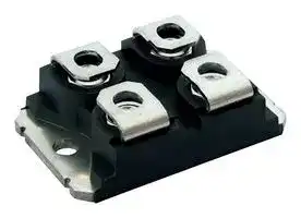
## **SOT-227 Silicon Carbide Single Phase Bridge, 50 A**
## **FEATURES**
- Virtually no recovery tail and no switching losses
- Majority carrier diode using Schottky technology on SiC wide band gap material
- Improved VF and efficiency by thin wafer technology
- High speed switching, low switching losses
- Positive temperature coefficient, for easy paralleling
**==> picture [34 x 7] intentionally omitted <==**
**----- Start of picture text -----**<br>
SOT-227<br>**----- End of picture text -----**<br>
- Electrically isolated base plate
- Large creepage distance between terminal
## **LINKS TO ADDITIONAL RESOURCES**
- Simplified mechanical designs, rapid assembly
- Designed and qualified for industrial level
Application Notes
- UL approved file E78996
- Material categorization: for definitions of compliance please see www.vishay.com/doc?99912
## **PRIMARY CHARACTERISTICS**
|**PRIMARY CHARACTERISTICS**|**PRIMARY CHARACTERISTICS**|
|---|---|
|IOat TC= 124 °C|50 A|
|VRRM|650 V|
|VFMat 50 A, TC= 25 °C|1.5 V|
|Package|SOT-227|
|Circuit configuration|Single phase bridge|
## **DESCRIPTION / APPLICATIONS**
Wide band gap SiC based 650 V Schottky diode, designed for high performance and ruggedness.
Optimum choice for high speed hard switching and efficient operation over a wide temperature range, it is also recommended for all applications suffering from Silicon ultrafast recovery behavior.
Typical applications include AC/DC PFC and DC/DC ultra high frequency output rectification in FBPS and LLC converters
## **MAJOR RATINGS AND CHARACTERISTICS**
|**MAJOR RATINGS AND CHARACTERISTICS**|**MAJOR RATINGS AND CHARACTERISTICS**|**MAJOR RATINGS AND CHARACTERISTICS**|**MAJOR RATINGS AND CHARACTERISTICS**|
|---|---|---|---|
|**SYMBOL**|**CHARACTERISTICS**|**VALUES**|**UNITS**|
|IO|180° rect. conduction angle|50|A|
||TC|124|°C|
|IFSM|50 Hz|267|A|
||60 Hz|280||
|I2t|50 Hz|358|A2s|
||60 Hz|327||
|VRRM||650|V|
|TJ||-40 to +175|°C|
## **ELECTRICAL SPECIFICATIONS**
## **VOLTAGE RATINGS**
||**VRRM, MAXIMUM REPETITIVE**|**VRSM, MAXIMUM NON-REPETITIVE PEAK**|
|---|---|---|
|**TYPE NUMBER**|**PEAK REVERSE VOLTAGE**|**REVERSE VOLTAGE**|
||**V**|**V**|
|VS-SC50BA65|650|650|
Revision: 22-Apr-2024
Document Number: 97173
**1**
For technical questions within your region: DiodesAmericas@vishay.com, DiodesAsia@vishay.com, DiodesEurope@vishay.com THIS DOCUMENT IS SUBJECT TO CHANGE WITHOUT NOTICE. THE PRODUCTS DESCRIBED HEREIN AND THIS DOCUMENT ARE SUBJECT TO SPECIFIC DISCLAIMERS, SET FORTH AT www.vishay.com/doc?91000
**VS-SC50BA65**
Vishay Semiconductors
www.vishay.com
## **ELECTRICAL SPECIFICATIONS** (TJ = 25 °C unless otherwise specified)
|**ELECTRICAL SPECIFICATIONS**(TJ= 25 °C unless otherwise specified)|**ELECTRICAL SPECIFICATIONS**(TJ= 25 °C unless otherwise specified)|**ELECTRICAL SPECIFICATIONS**(TJ= 25 °C unless otherwise specified)|**ELECTRICAL SPECIFICATIONS**(TJ= 25 °C unless otherwise specified)|**ELECTRICAL SPECIFICATIONS**(TJ= 25 °C unless otherwise specified)|**ELECTRICAL SPECIFICATIONS**(TJ= 25 °C unless otherwise specified)|**ELECTRICAL SPECIFICATIONS**(TJ= 25 °C unless otherwise specified)|
|---|---|---|---|---|---|---|
|**PARAMETER**|**SYMBOL**|**TEST CONDITIONS**|**MIN.**|**TYP.**|**MAX.**|**UNITS**|
|Cathode to anode breakdown voltage|VBR|IR= 200 μA|650|-|-|V|
|Forward voltage|VFM|IF= 50 A||1.5|1.73||
|||IF= 50 A, TJ= 150 °C|-|1.88|-||
|Reverse leakage current|IRM|VR= 650 V|-|1.9|80|μA|
|||TJ= 125 °C, VR= 650 V|-|6.0|-||
|||TJ= 150 °C, VR= 650 V|-|9.0|-||
|Junction capacitance|CT|VR= 650 V, f = 1 MHz|-|161|-|pF|
|RMS isolation voltage base plate|VISOL|f = 50 Hz, any terminal to case, t = 1 min.|2500|-|-|V|
## **FORWARD CONDUCTION**
|**FORWARD CONDUCTION**|**FORWARD CONDUCTION**|**FORWARD CONDUCTION**|**FORWARD CONDUCTION**|**FORWARD CONDUCTION**|**FORWARD CONDUCTION**|**FORWARD CONDUCTION**|
|---|---|---|---|---|---|---|
|**PARAMETER**|**SYMBOL**|**TEST CONDITIONS**|||**VALUES**|**UNITS**|
|Maximum DC output current<br>at case temperature|IO|Resistive or inductive load|||50|A|
||||||124|°C|
|Maximum peak, one-cycle<br>non-repetitive forward current|IFSM|t = 10 ms|No voltage<br>reapplied|Initial TJ= 25 °C|267|A|
|||t = 8.3 ms|||280||
|||t = 10 ms|100 % VRRM<br>reapplied||225||
|||t = 8.3 ms|||235||
|Maximum I2t for fusing|I2t|t = 10 ms|No voltage<br>reapplied||358|A2s|
|||t = 8.3 ms|||327||
|||t = 10 ms|100 % VRRM<br>reapplied||253||
|||t = 8.3 ms|||231||
|Maximum I2√t for fusing|I2√t|I2t for time tx= I2√t x√tx;0.1≤tx ≤10 ms, VRRM= 0 V|||3.58|kA2√s|
|Low level of threshold voltage, per leg|VF(T0)1|(16.7 % xπx IF(AV)) < I <πx IF(AV), TJ= TJmaximum|||0.87|V|
|Low level value of forward slope resistance|rf1||||25.47|mΩ|
|High level of threshold voltage, per leg|VF(T0)2|(I >πx IF(AV)), TJ= TJmaximum|||0.98|V|
|High level value of forward slope resistance|rf2||||25.19|mΩ|
|Maximum forward voltage, per diode|VFM|IF= 50 A|||1.73|V|
## **DYNAMIC RECOVERY CHARACTERISTICS** (TJ = 25 °C unless otherwise specified)
|**DYNAMIC RECOVERY CHARACTERISTICS**(TJ= 25 °C unless otherwise specified)|**DYNAMIC RECOVERY CHARACTERISTICS**(TJ= 25 °C unless otherwise specified)|**DYNAMIC RECOVERY CHARACTERISTICS**(TJ= 25 °C unless otherwise specified)|**DYNAMIC RECOVERY CHARACTERISTICS**(TJ= 25 °C unless otherwise specified)|**DYNAMIC RECOVERY CHARACTERISTICS**(TJ= 25 °C unless otherwise specified)|**DYNAMIC RECOVERY CHARACTERISTICS**(TJ= 25 °C unless otherwise specified)|**DYNAMIC RECOVERY CHARACTERISTICS**(TJ= 25 °C unless otherwise specified)|
|---|---|---|---|---|---|---|
|**PARAMETER**|**SYMBOL**|**TEST CONDITIONS**|**MIN.**|**TYP.**|**MAX.**|**UNITS**|
|Total capacitive charge|QC|VR= 400 V|-|110|-|nC|
## **THERMAL - MECHANICAL SPECIFICATIONS**
|**THERMAL - MECHANICAL SPECIFICATIONS**|**THERMAL - MECHANICAL SPECIFICATIONS**|**THERMAL - MECHANICAL SPECIFICATIONS**|**THERMAL - MECHANICAL SPECIFICATIONS**|**THERMAL - MECHANICAL SPECIFICATIONS**|**THERMAL - MECHANICAL SPECIFICATIONS**|**THERMAL - MECHANICAL SPECIFICATIONS**|
|---|---|---|---|---|---|---|
|**PARAMETER**|**SYMBOL**|**TEST CONDITIONS**|**MIN.**|**TYP.**|**MAX.**|**UNITS**|
|Thermal resistance junction-to-case,<br>per diode|RthJC||-|-|0.94|°C/W|
|Case-to-heatsink|RthCS|Flat, greased surface|-|0.1|-||
|Weight|||-|30|-|g|
|Mounting torque||Torque to terminal|-|-|1.1 (9.7)|Nm (lbf.in)|
|||Torque to heatsink|-|-|1.8 (15.9)|Nm (lbf.in)|
|Case style|||SOT-227||||
Revision: 22-Apr-2024
Document Number: 97173
**2**
For technical questions within your region: DiodesAmericas@vishay.com, DiodesAsia@vishay.com, DiodesEurope@vishay.com THIS DOCUMENT IS SUBJECT TO CHANGE WITHOUT NOTICE. THE PRODUCTS DESCRIBED HEREIN AND THIS DOCUMENT ARE SUBJECT TO SPECIFIC DISCLAIMERS, SET FORTH AT www.vishay.com/doc?91000
**VS-SC50BA65** Vishay Semiconductors
**==> picture [506 x 426] intentionally omitted <==**
**----- Start of picture text -----**<br>
www.vishay.com Vishay Semiconductors<br>a a<br>Axis Title Axis Title<br>80 10000 160 10000<br>70 P| TJ = 175 °C | ULL LT 140 P| | | | |<br>TJ = 150 °C<br>60 | TJ = 125 °C 7A 120 P| | | |YAYA<br>50 | T J = 25 ° C rYf |_| 1000 100 P| | |efef 1000<br>40 80<br>| [fi | | et ft<br>30 | | | fF | | 60 P| [[wil]]<br>100 100<br>20 | | [Ff | 40 LY Tf = 1.0 MHzJ = 25 °Cf = 1.0 MHzJ = 25 °CJ = 25 °C = 25 °C | i<br>10 20<br>| | |<br>0 | | [A|| [| | [ | | 10 0 fyABRs|ABRs|| | | [cw{oe{oe 10<br> 0 0.5 1.0 1.5 2.0 2.5 3.0 0 100 200 300 400 500 600 700<br>VF - Forward Voltage Drop (V) Reverse Voltage (V)<br>Fig. 1 - Typical Forward Voltage Drop Characteristics Fig. 4 - Typical Capacitive Charge vs. Reverse Voltage<br>Axis Title Axis Title<br>0.01 10000 180 10000<br>160<br>| TJ = 175 ° C 140<br>T J = 150 °C<br>rT T J = 125 °C _ fy} 1000 120 IN 180° rect. 1000<br>TJ = 25 °C ZH 100 See 180° sine NGaaEe<br>0.001 | || LH | | 80 } iN\\ L<br>ot oH TS 100 60 WN 100<br>eee 40 PELL<br>20<br>Cee PEELE<br>0.0001 | Zeer 10 0 FLEEOeOe 10<br>0 100 200 300 400 500 600 700 0 10 20 30 40 50 60 70 80 90 100<br>VR - Reverse Voltage (V) IOO - Total Output Current (A)<br>(nC)<br>line line<br>Charge<br>2nd line 1st line 2nd line 2nd 1st line 2nd<br>Capacitive<br> - Instantaneous Forward Current (A)IF<br>2nd line 1st line 2nd line 2nd line 1st line 2nd line<br> - Reverse Current (µA)<br>IR<br>Maximum Allowable Case Temperature (°C)<br>**----- End of picture text -----**<br>
**==> picture [190 x 572] intentionally omitted <==**
**----- Start of picture text -----**<br>
160<br>140 P| | | | |<br>120<br>P| | | |YAYA<br>100 P| | |efef<br>80<br>| et ft<br>60 P| [[wil]]<br>40 LY Tf = 1.0 MHzJ = 25 °Cf = 1.0 MHzJ = 25 °CJ = 25 °C = 25 °C | i<br>20<br>| |<br>0 fyABRs|ABRs|| | | [cw{oe{oe<br>0 100 200 300 400 500 600 700<br>Reverse Voltage (V)<br>Fig. 4 - Typical Capacitive Charge vs. Reverse Voltage<br>Axis Title<br>180<br>160<br>140<br>120 IN 180° rect.<br>100 See 180° sine NGaaEe<br>80 } iN\\ L<br>60 WN<br>40 PELL<br>20<br>PEELE<br>0 FLEEOeOe<br>0 10 20 30 40 50 60 70 80 90 100<br>IOO - Total Output Current (A)<br>Fig. 5 - Maximum Allowable Case Temperature vs.<br> Average Forward Current<br>Axis Title<br>900<br>800<br>700<br>600<br>500 PEPE 180° sine AZ<br>400<br>180° rect.<br>300 K/<br>200 EEE AE<br>100 TT<br>0 CTLAS COLE<br>0 10 20 30 40 50 60 70 80 90 100<br>IO - Total Output Current (A)<br>(nC)<br>Charge<br>Capacitive<br>Maximum Allowable Case Temperature (°C)<br>Maximum Total Power Loss (W)<br>**----- End of picture text -----**<br>
Fig. 5 - Maximum Allowable Case Temperature vs. Average Forward Current
Fig. 2 - Typical Values of Reverse Current vs. Reverse Voltage
**==> picture [191 x 160] intentionally omitted <==**
**----- Start of picture text -----**<br>
10 000<br>a ae a<br>SE<br>1000<br>eee Ce SS<br>pone ek NE<br>CN FCI FEMS<br>100 LLIN LE CEI ta<br>0.1 1 10 100 1000<br>VR - Reverse Voltage (V)<br>C - Junction Capacitance (pF)T<br>**----- End of picture text -----**<br>
**==> picture [160 x 9] intentionally omitted <==**
**----- Start of picture text -----**<br>
Fig. 6 - Forward Power Loss Characteristics<br>**----- End of picture text -----**<br>
Fig. 3 - Junction Capacitance vs. Reverse Voltage
Revision: 22-Apr-2024
Document Number: 97173
**3**
For technical questions within your region: DiodesAmericas@vishay.com, DiodesAsia@vishay.com, DiodesEurope@vishay.com THIS DOCUMENT IS SUBJECT TO CHANGE WITHOUT NOTICE. THE PRODUCTS DESCRIBED HEREIN AND THIS DOCUMENT ARE SUBJECT TO SPECIFIC DISCLAIMERS, SET FORTH AT www.vishay.com/doc?91000
**VS-SC50BA65**
www.vishay.com
## Vishay Semiconductors
**==> picture [209 x 159] intentionally omitted <==**
**----- Start of picture text -----**<br>
270 10000<br>240 Initial T Rated VJ = 25 RRM reapplied° C<br>210<br>at 60 Hz 0.0083 s 1000<br>180<br>at 50 Hz 0.01 s<br>150<br>120<br>100<br>90<br>60<br>30 10<br>1 10 100<br>Number of Equal Amplitude Half Cycle Current Pulses (N)<br> (A)<br>IFSM<br>**----- End of picture text -----**<br>
Fig. 7 - Non-Repetitive Peak Forward Surge Current vs. Number Pulses
**==> picture [186 x 161] intentionally omitted <==**
**----- Start of picture text -----**<br>
300<br>Initial TJ = 25 °C<br>270<br>240<br>210 V R = 0<br>180 V R = V RRM<br>150<br>120<br>90<br>60<br>30<br>0.01 0.1 1<br>tp (s)<br> (A)<br>IFSM<br>**----- End of picture text -----**<br>
Fig. 8 - Non-Repetitive Peak Forward Surge Current vs. Pulse Duration
**==> picture [462 x 160] intentionally omitted <==**
**----- Start of picture text -----**<br>
1<br>0.1<br>0.50<br>0.20<br>0.10<br>0.05<br>0.02<br>0.01<br>0.01<br>0.001<br>0.00001 0.0001 0.001 0.01 0.1 1 10<br>t1 - Rectangular Pulse Duration (s)<br> - Thermal Impedance<br>thJC Junction to Case (°C/W)<br>Z<br>**----- End of picture text -----**<br>
Fig. 9 - Maximum Thermal Impedance Characteristics
Revision: 22-Apr-2024
Document Number: 97173
**4**
For technical questions within your region: DiodesAmericas@vishay.com, DiodesAsia@vishay.com, DiodesEurope@vishay.com THIS DOCUMENT IS SUBJECT TO CHANGE WITHOUT NOTICE. THE PRODUCTS DESCRIBED HEREIN AND THIS DOCUMENT ARE SUBJECT TO SPECIFIC DISCLAIMERS, SET FORTH AT www.vishay.com/doc?91000
**VS-SC50BA65**
Vishay Semiconductors
www.vishay.com
## **ORDERING INFORMATION TABLE**
|**Device code**|**VS-**|**VS-**||**S**<br>**C**<br>**50**<br>**B**|**S**<br>**C**<br>**50**<br>**B**|**S**<br>**C**<br>**50**<br>**B**|**A**|**65**||
|---|---|---|---|---|---|---|---|---|---|
||1|||5<br>3<br>2<br>4|||6|7||
||**1**||-||Vishay Semiconductors product|||||
||**2**||-||Silicon Carbide diode|||||
||**3**||-||Present silicon generation|||||
||**4**||-||Current rating (50 = 50|A)||||
||**5**||-||Circuit configuration (single phase|||bridge)||
||**6**||-||Package indicator (SOT-227 standard insulated base)|||||
||**7**||-||Voltage rating (65 = 650 V)|||||
Quantity per tube is 10, M4 screw and washer included
|**CIRCUIT CONFIGURATION**|**CIRCUIT CONFIGURATION**|**CIRCUIT CONFIGURATION**||||||||||
|---|---|---|---|---|---|---|---|---|---|---|---|
|**CIRCUIT**|**CIRCUIT CONFIGURATION CODE**||**CIRCUIT DRAWING**|||||||||
|Single phase bridge|B|(AC) 4<br>(+) 1|||||1<br>4<br>Lead Assignment<br>2 (AC)<br>3 (-)||||3<br>2|
|||||||||||||
|||||||||||||
|||||||||||||
|||||||||||||
|||||||||||||
|||||||||||||
|||||||||||||
|||||||||||||
|||||||||||||
|||||||||||||
|||||||||||||
|**LINKS TO RELATED DOCUMENTS**||||||||||||
|Dimensions|||||www.vishay.com/doc?95423|||||||
|Part marking information|||||www.vishay.com/doc?95425|||||||
Revision: 22-Apr-2024
Document Number: 97173
**5**
For technical questions within your region: DiodesAmericas@vishay.com, DiodesAsia@vishay.com, DiodesEurope@vishay.com THIS DOCUMENT IS SUBJECT TO CHANGE WITHOUT NOTICE. THE PRODUCTS DESCRIBED HEREIN AND THIS DOCUMENT ARE SUBJECT TO SPECIFIC DISCLAIMERS, SET FORTH AT www.vishay.com/doc?91000
**Legal Disclaimer Notice** Vishay
www.vishay.com
## **Disclaimer**
ALL PRODUCT, PRODUCT SPECIFICATIONS AND DATA ARE SUBJECT TO CHANGE WITHOUT NOTICE TO IMPROVE RELIABILITY, FUNCTION OR DESIGN OR OTHERWISE.
Vishay Intertechnology, Inc., its affiliates, agents, and employees, and all persons acting on its or their behalf (collectively, “Vishay”), disclaim any and all liability for any errors, inaccuracies or incompleteness contained in any datasheet or in any other disclosure relating to any product.
Vishay makes no warranty, representation or guarantee regarding the suitability of the products for any particular purpose or the continuing production of any product. To the maximum extent permitted by applicable law, Vishay disclaims (i) any and all liability arising out of the application or use of any product, (ii) any and all liability, including without limitation special, consequential or incidental damages, and (iii) any and all implied warranties, including warranties of fitness for particular purpose, non-infringement and merchantability.
Statements regarding the suitability of products for certain types of applications are based on Vishay's knowledge of typical requirements that are often placed on Vishay products in generic applications. Such statements are not binding statements about the suitability of products for a particular application. It is the customer's responsibility to validate that a particular product with the properties described in the product specification is suitable for use in a particular application. Parameters provided in datasheets and / or specifications may vary in different applications and performance may vary over time. All operating parameters, including typical parameters, must be validated for each customer application by the customer's technical experts. Product specifications do not expand or otherwise modify Vishay's terms and conditions of purchase, including but not limited to the warranty expressed therein.
Hyperlinks included in this datasheet may direct users to third-party websites. These links are provided as a convenience and for informational purposes only. Inclusion of these hyperlinks does not constitute an endorsement or an approval by Vishay of any of the products, services or opinions of the corporation, organization or individual associated with the third-party website. Vishay disclaims any and all liability and bears no responsibility for the accuracy, legality or content of the third-party website or for that of subsequent links.
Except as expressly indicated in writing, Vishay products are not designed for use in medical, life-saving, or life-sustaining applications or for any other application in which the failure of the Vishay product could result in personal injury or death. Customers using or selling Vishay products not expressly indicated for use in such applications do so at their own risk. Please contact authorized Vishay personnel to obtain written terms and conditions regarding products designed for such applications.
No license, express or implied, by estoppel or otherwise, to any intellectual property rights is granted by this document or by any conduct of Vishay. Product names and markings noted herein may be trademarks of their respective owners.
_**© 2024 VISHAY INTERTECHNOLOGY, INC. ALL RIGHTS RESERVED**_
Revision: 01-Jan-2024
Document Number: 91000
**1** For technical questions, contact: THIS DOCUMENT IS SUBJECT TO CHANGE WITHOUT NOTICE. THE PRODUCTS DESCRIBED HEREIN AND THIS DOCUMENT ARE SUBJECT TO SPECIFIC DISCLAIMERS, SET FORTH AT www.vishay.com/doc?91000
Updated at April 22, 2026
Vishay is a global leader in the manufacturing of discrete semiconductors and passive electronic components. Renowned for its exceptional quality and engineering expertise, the company produces highly reliable solutions that drive innovation across the industrial, automotive, telecommunications, and consumer electronics markets. From advanced factory automation to vehicle electrification, Vishay components provide the foundational building blocks for modern electronic design. The company's expansive portfolio is heavily focused on efficient power management, signal routing, and energy storage. Within its passive component lineup, Vishay is recognized for its extensive array of high-performance capacitors, including robust aluminium electrolytic, film, and polymer variants, alongside highly efficient power inductors. In the realm of discrete semiconductors, Vishay is a premier manufacturer of single and dual MOSFETs, as well as a vast selection of Schottky, Zener, and fast-recovery rectifier diodes designed for demanding power applications. Furthermore, Vishay delivers industry-leading circuit protection and thermal management solutions. With a broad offering of transient voltage suppressors (TVS diodes) and temperature-sensing NTC thermistors, these components are engineered to safeguard sensitive circuitry against both electrical and thermal overstress. By combining this vital mix of advanced discretes and passives, Vishay enables engineers to develop robust, space-saving, and highly resilient electronic systems.
About Novapart
Novapart is a B2B electronic component broker specialising in stock shortages and cost reduction. We source hard-to-find parts and identify compliant alternatives across a catalogue of 540,000+ components from 500+ manufacturers.
Learn more →Stock Shortage Specialist
When a component is unavailable, discontinued or has an unacceptable lead time, we tap into our network of vetted European and Asian distributors to source what you need — without compromising on quality or traceability.
Request a quote →Compliant Alternatives
We identify pin-to-pin, electrically equivalent substitutes that meet the same certifications (RoHS, AEC-Q100, REACH) as your original specification — validated against datasheets, not just part numbers. Often at a lower cost.
BOM Analysis service →