


VS-C20ET07T-M3
Silicon Carbide Schottky Diode, Single, 650 V, 20 A, 68 nC, TO-220AC
- Manufacturer: VISHAY
- Product type: Silicon Carbide Schottky Diodes
- Available until stocks are exhausted
- SVHC: To Be Advised
- No. of Pins: 2 Pin
- Product Range: -
- Qualification: -
- Diode Mounting: Through Hole
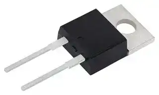
- Diode Case Style: TO-220AC
- Diode Configuration: Single
- Average Forward Current: 20A
- Total Capacitive Charge: 68nC
- Operating Temperature Max: 175°C
- Repetitive Peak Reverse Voltage: 650V
| Delivery and price | |
|---|---|
| Units per pack | 250 |
| Price | 3.58 € |
| Current stock | 500+ |
| Lead time | 30 days |
**VS-C20ET07T-M3** www.vishay.com ## Vishay Semiconductors ## **650 V Power SiC Merged PIN Schottky Diode, 20 A** ## **FEATURES** **==> picture [221 x 87] intentionally omitted <==** **----- Start of picture text -----**<br> Base cathode<br>2<br>e 2<br>1<br>1 3<br>3 Cathode Anode<br> 2L TO-220AC<br>**----- End of picture text -----**<br> ## **LINKS TO ADDITIONAL RESOURCES** ~~CE]~~ SPICE 3D Models Models Application Notes - Majority carrier diode using Schottky technology on SiC wide band gap material - Positive VF temperature coefficient for easy paralleling - Virtually no recovery tail and no switching losses - Temperature invariant switching behavior - 175 °C maximum operating junction temperature - MPS structure for high ruggedness to forward current surge events - Meets JESD 201 class 1A whisker test - Solder Bath temperature 275 °C maximum, 10 s per JESD 22-B106 - Material categorization: for definitions of compliance please see www.vishay.com/doc?99912 ## **PRIMARY CHARACTERISTICS** |**PRIMARY CHARACTERISTICS**|**PRIMARY CHARACTERISTICS**| |---|---| |IF(AV)|20 A| |VR|650 V| |VFat IFat 150 °C|1.6 V| |TJmax.|175 °C| |IRat VRat 175 °C|35 μA| |QC(VR= 400 V)|68 nC| |Package|2L TO-220AC| |Circuit configuration|Single| ## **DESCRIPTION / APPLICATIONS** Wide band gap SiC based 650 V Schottky diode, designed for high performance and ruggedness. Optimum choice for high speed hard switching and efficient operation over a wide temperature range, it is also recommended for all applications suffering from Silicon ultrafast recovery behavior. Typical applications include AC/DC PFC and DC/DC ultra high frequency output rectification in FBPS and LLC converters. ## **MECHANICAL DATA** **Case:** 2L TO-220AC Molding compound meets UL 94 V-0 flammability rating Base P/N-M3 - halogen-free, RoHS-compliant **Terminals:** matte tin plated leads, solderable per J-STD-002 and JESD 22-B102 **Mounting torque:** 10 in-lbs maximum |**ABSOLUTE MAXIMUM RATINGS**(TA= 25 °C unless otherwise specified)<br>~~Cn~~|**ABSOLUTE MAXIMUM RATINGS**(TA= 25 °C unless otherwise specified)<br>~~Cn~~|**ABSOLUTE MAXIMUM RATINGS**(TA= 25 °C unless otherwise specified)<br>~~Cn~~|**ABSOLUTE MAXIMUM RATINGS**(TA= 25 °C unless otherwise specified)<br>~~Cn~~|**ABSOLUTE MAXIMUM RATINGS**(TA= 25 °C unless otherwise specified)<br>~~Cn~~| |---|---|---|---|---| |**PARAMETER**<br>~~GGG~~|**SYMBOL**<br>~~GGG~~|**TEST CONDITIONS**<br>~~GGG~~|**VALUES**<br>~~GGG~~|**UNITS**<br>~~GGG~~| |Peak repetitive reverse voltage<br>~~DGG~~|VRRM<br>~~DGG~~|~~DGG~~|650<br>~~DGG~~|V<br>~~DGG~~| |Average rectified forward current<br>~~GGG~~|IF(AV)<br>~~GGG~~|TC= 125 °C (DC)<br>~~GGG~~|20<br>~~GGG~~|A<br>~~GGG~~| |DC blockingvoltage<br>~~GGG~~|VDC<br>~~GGG~~|~~GGG~~|650<br>~~GGG~~|V<br>~~GGG~~| |Repetitive peak surge current<br>~~a~~|IFRM<br>~~BG~~|TC= 25 °C, f = 50 Hz, square wave, DC = 25 %<br>~~BG~~|75<br>~~BG~~|A<br>~~eee~~| |Non-repetitive peak forward surge current<br>~~Lf~~<br><br>~~I~~|IFSM<br>~~Lf~~<br>~~cs~~<br>~~I~~|TC= 25 °C, tp= 10 ms, half sine wave<br>~~Lf~~|160<br>~~Lf~~|| |||TC= 110 °C, tp= 10 ms, half sine wave<br>~~Lf~~<br>~~|~~<br>~~cs~~<br>|140<br>~~Lf~~<br>~~|~~<br>~~eee~~<br>|| |Power dissipation<br>~~a ~~<br>~~I~~|Ptot (1)<br> ~~cs~~<br>~~I~~|TC= 25 °C<br>~~|~~<br>~~pT~~<br>~~cs~~<br>|119<br>~~|~~<br>~~eee~~<br>|W<br>~~eee~~| |||TC= 110 °C<br>~~|~~<br>~~pT~~<br>~~cs~~<br>|52<br>~~|~~<br>~~eee~~<br>|| |I2t value<br> <br>~~I~~|i2 t<br>d<br><br> ~~cs~~<br>~~I ~~|TC= 25 °C<br>~~cs~~<br>|128<br>~~eee~~<br>|A2s<br>~~eee~~| |||TC= 110 °C<br>~~cs ~~<br> ~~ee~~|98<br> ~~eee~~<br>~~ee~~|| |Operatingjunction and storage temperatures<br>~~GC~~|TJ(2), TStg<br>~~GC~~|~~GC~~|-55 to +175<br>~~GC~~|°C<br>~~GC~~| > (2) The heat generated must be less than the thermal conductivity from junction-to-ambient: dPD/dTJ < 1/RθJA Revision: 16-Apr-2021 Document Number: 96726 **1** For technical questions within your region: DiodesAmericas@vishay.com, DiodesAsia@vishay.com, DiodesEurope@vishay.com THIS DOCUMENT IS SUBJECT TO CHANGE WITHOUT NOTICE. THE PRODUCTS DESCRIBED HEREIN AND THIS DOCUMENT ARE SUBJECT TO SPECIFIC DISCLAIMERS, SET FORTH AT www.vishay.com/doc?91000 **VS-C20ET07T-M3** www.vishay.com ## Vishay Semiconductors |**ELECTRICAL SPECIFICATIONS**(TJ=|**ELECTRICAL SPECIFICATIONS**(TJ=|25 °C unless otherwise specified)|25 °C unless otherwise specified)|25 °C unless otherwise specified)|25 °C unless otherwise specified)|25 °C unless otherwise specified)| |---|---|---|---|---|---|---| |**PARAMETER**|**SYMBOL**|**TEST CONDITIONS**|**MIN.**|**TYP.**|**MAX.**|**UNITS**| |Forward voltage|VF|IF= 20 A|-|1.45|1.70|V| |||IF= 20 A, TJ= 150 °C|-|1.60|1.90|| |||IF= 20 A, TJ= 175 °C|-|1.65|-|| |Reverse leakage current|IR|VR= VRrated|-|-|100|μA| |||VR= VRrated, TJ= 150 °C|-|-|250|| |||VR= VRrated, TJ= 175 °C|-|35|-|| |Total capacitance|C|VR= 1 V, f = 1 MHz|-|1050|-|pF| |||VR= 400 V, f = 1 MHz|-|105|-|| |Total capacitive charge|QC|VR= 400 V, f = 1 MHz|-|68|-|nC| |**THERMAL - MECHANICAL SPECIFICATIONS**(TA= 25 °C unless otherwise specified)|**THERMAL - MECHANICAL SPECIFICATIONS**(TA= 25 °C unless otherwise specified)|**THERMAL - MECHANICAL SPECIFICATIONS**(TA= 25 °C unless otherwise specified)|**THERMAL - MECHANICAL SPECIFICATIONS**(TA= 25 °C unless otherwise specified)|**THERMAL - MECHANICAL SPECIFICATIONS**(TA= 25 °C unless otherwise specified)|**THERMAL - MECHANICAL SPECIFICATIONS**(TA= 25 °C unless otherwise specified)|**THERMAL - MECHANICAL SPECIFICATIONS**(TA= 25 °C unless otherwise specified)| |---|---|---|---|---|---|---| |**PARAMETER**|**SYMBOL**|**TEST CONDITIONS**|**MIN.**|**TYP.**|**MAX.**|**UNITS**| |Thermal resistance, junction-to-case|RthJC||-|0.9|1.3|°C/W| |Markingdevice|||C20ET07T|||| **==> picture [210 x 362] intentionally omitted <==** **----- Start of picture text -----**<br> 40 10000<br>35<br>30 TJ = 25 °C<br>1000<br>25 T J = -55 °C<br>TJ = 125 °C<br>20 T J = 150 °C<br>TJ = 175 °C<br>15<br>100<br>10<br>5<br>0 10<br>0 0.5 1.0 1.5 2.0 2.5 3.0<br>VF - Forward Voltage Drop (V)<br>Fig. 1 - Typical Forward Voltage Drop Characteristics<br>Axis Title<br>100 10000<br>10<br>1000<br>1 TJ = 175 ° C<br>0.1 T J = 150 °C<br>100<br>0.01 TT J J = 125 °C= 25 °C<br>TJ = -55 °C<br>0.001 10<br>0 100 200 300 400 500 600 700<br>VR - Reverse Voltage (V)<br> - Instantaneous Forward Current (A)IF<br> - Reverse Current (µA)<br>IR<br>**----- End of picture text -----**<br> Fig. 2 - Typical Values of Reverse Current vs. Reverse Voltage **==> picture [210 x 362] intentionally omitted <==** **----- Start of picture text -----**<br> 10 000 10000<br>1000 1000<br>100 100<br>T J = 25 °C<br>f = 1.0 MHz<br>10 10<br>0.1 1 10 100 1000<br>VR - Reverse Voltage (V)<br>Fig. 3 - Typical Junction Capacitance vs. Reverse Voltage<br>Axis Title<br>1000 10000<br>T J = 25 °C<br>1000<br>TJ = 110 °C<br>100<br>100<br>10 10<br>0.0001 0.001 0.01<br>tp (s)<br>C - Junction Capacitance (pF)T<br> (A)<br>IFSM<br>**----- End of picture text -----**<br> Fig. 3 - Typical Junction Capacitance vs. Reverse Voltage Fig. 4 - Non-Repetitive Peak Forward Surge Current vs. Pulse Duration (Square Wave) Revision: 16-Apr-2021 Document Number: 96726 **2** For technical questions within your region: DiodesAmericas@vishay.com, DiodesAsia@vishay.com, DiodesEurope@vishay.com THIS DOCUMENT IS SUBJECT TO CHANGE WITHOUT NOTICE. THE PRODUCTS DESCRIBED HEREIN AND THIS DOCUMENT ARE SUBJECT TO SPECIFIC DISCLAIMERS, SET FORTH AT www.vishay.com/doc?91000 **VS-C20ET07T-M3** **==> picture [77 x 10] intentionally omitted <==** **----- Start of picture text -----**<br> www.vishay.com<br>**----- End of picture text -----**<br> ## Vishay Semiconductors **==> picture [464 x 581] intentionally omitted <==** **----- Start of picture text -----**<br> 1<br>PS A<br>eS ee US<br>0.1<br>D = 0.5<br>D = 0.2<br>SCRE SS D = 0.1 er<br>D = 0.05<br>D = 0.02<br>D = 0.01<br>DC<br>0.01 EoSee att<br>nS See<br>0.00001 0.0001 0.001 0.01 0.1 1 10<br>t1 - Rectangular Pulse Duration (s)<br>Fig. 5 - Typical Thermal Impedance ZthJC Characteristics<br>Axis Title Axis Title<br>175 10000 30<br>150 25<br>125 pSNe| 1000 20 pt tttT<br>100 15<br>Pp} Pf itt Ty<br>75 100 10<br>P| pt tt | Yt |<br>TJ = 25 °C<br>f = 1.0 MHz<br>50 5<br>P| | Sea<br>25 po| 10 0 peeeee’here<br>0 5 10 15 20 25 0 100 200 300 400 500 600 700<br>IF(AV) - Average Forward Output Current (A) Reverse Voltage (V)<br>Fig. 6 - Maximum Allowable Case Temperature vs. Fig. 8 - Typical Capacitive Energy vs. Reverse Voltage<br>Average Forward Current<br>Axis Title Axis Title<br>180 10000 100<br>160<br>140 INNESS E S 80 P| i | | LZee<br>120 1000<br>SERRE 60 Coop<br>100 R thJC typ.<br>80 So -<br>PSA 40 EDpZannE<br>60 R thJC max. 100 TJ = 25 °C<br>40 PO S NA 20 Vann/ f = 1.0 MHz<br>20<br>ee eee / 0.=f'cav<br>0 10 0<br>25 50 75 100 125 150 175 0 100 200 300 400 500 600 700<br>Case Temperature (°C) Reverse Voltage (V)<br> - Thermal Impedance<br>thJC Junction to Case (°C/W)<br>Z<br>(µJ)<br>line Energy<br>2nd line 1st line 2nd line 2nd Capacitive<br>Allowable Case Temperature (°C)<br>(nC)<br>line<br>Charge<br>2nd line 1st line 2nd line 2nd<br>Capacitive<br>Allowable Input Power (W)<br>**----- End of picture text -----**<br> Fig. 8 - Typical Capacitive Energy vs. Reverse Voltage Fig. 7 - Forward Power Loss Characteristics **==> picture [195 x 9] intentionally omitted <==** **----- Start of picture text -----**<br> Fig. 9 - Typical Capacitive Charge vs. Reverse Voltage<br>**----- End of picture text -----**<br> Revision: 16-Apr-2021 Document Number: 96726 **3** For technical questions within your region: DiodesAmericas@vishay.com, DiodesAsia@vishay.com, DiodesEurope@vishay.com THIS DOCUMENT IS SUBJECT TO CHANGE WITHOUT NOTICE. THE PRODUCTS DESCRIBED HEREIN AND THIS DOCUMENT ARE SUBJECT TO SPECIFIC DISCLAIMERS, SET FORTH AT www.vishay.com/doc?91000 **VS-C20ET07T-M3** www.vishay.com ## Vishay Semiconductors ## **ORDERING INFORMATION TABLE** **==> picture [391 x 203] intentionally omitted <==** **----- Start of picture text -----**<br> Device code VS- C 20 E T 07 T -M3<br>1 2 3 4 5 6 7 8<br>1 - Vishay Semiconductors product<br>2 - C = SiC diode<br>3 - Current rating (20 = 20 A)<br>4 - E = single diode<br>5 - Package TO-220<br>6 - Voltage rating: (07 = 650 V)<br>7 - T = true 2 pin<br>8 - Environmental digit:<br>-M3 = halogen-free, RoHS-compliant, and termination lead (Pb)-free<br>**----- End of picture text -----**<br> |**ORDERING INFORMATION**|**ORDERING INFORMATION**|**ORDERING INFORMATION**|**ORDERING INFORMATION**|**ORDERING INFORMATION**| |---|---|---|---|---| |**PREFERRED P/N**|**BASE QUANTITY**|**MINIMUM ORDER QUANTITY**||**PACKAGING DESCRIPTION**| |VS-C20ET07T-M3|50/tube|1000||Antistatic plastic tubes| |||||| |**LINKS TO RELATED DOCUMENTS**||||| |Dimensions|||www.vishay.com/doc?96069|| |Part markinginformation|||www.vishay.com/doc?95391|| |SPICE model|||www.vishay.com/doc?96834|| Revision: 16-Apr-2021 Document Number: 96726 **4** For technical questions within your region: DiodesAmericas@vishay.com, DiodesAsia@vishay.com, DiodesEurope@vishay.com THIS DOCUMENT IS SUBJECT TO CHANGE WITHOUT NOTICE. THE PRODUCTS DESCRIBED HEREIN AND THIS DOCUMENT ARE SUBJECT TO SPECIFIC DISCLAIMERS, SET FORTH AT www.vishay.com/doc?91000 **Legal Disclaimer Notice** Vishay www.vishay.com ## **Disclaimer** ALL PRODUCT, PRODUCT SPECIFICATIONS AND DATA ARE SUBJECT TO CHANGE WITHOUT NOTICE TO IMPROVE RELIABILITY, FUNCTION OR DESIGN OR OTHERWISE. Vishay Intertechnology, Inc., its affiliates, agents, and employees, and all persons acting on its or their behalf (collectively, “Vishay”), disclaim any and all liability for any errors, inaccuracies or incompleteness contained in any datasheet or in any other disclosure relating to any product. Vishay makes no warranty, representation or guarantee regarding the suitability of the products for any particular purpose or the continuing production of any product. To the maximum extent permitted by applicable law, Vishay disclaims (i) any and all liability arising out of the application or use of any product, (ii) any and all liability, including without limitation special, consequential or incidental damages, and (iii) any and all implied warranties, including warranties of fitness for particular purpose, non-infringement and merchantability. Statements regarding the suitability of products for certain types of applications are based on Vishay’s knowledge of typical requirements that are often placed on Vishay products in generic applications. Such statements are not binding statements about the suitability of products for a particular application. It is the customer’s responsibility to validate that a particular product with the properties described in the product specification is suitable for use in a particular application. Parameters provided in datasheets and / or specifications may vary in different applications and performance may vary over time. All operating parameters, including typical parameters, must be validated for each customer application by the customer’s technical experts. Product specifications do not expand or otherwise modify Vishay’s terms and conditions of purchase, including but not limited to the warranty expressed therein. Except as expressly indicated in writing, Vishay products are not designed for use in medical, life-saving, or life-sustaining applications or for any other application in which the failure of the Vishay product could result in personal injury or death. Customers using or selling Vishay products not expressly indicated for use in such applications do so at their own risk. Please contact authorized Vishay personnel to obtain written terms and conditions regarding products designed for such applications. No license, express or implied, by estoppel or otherwise, to any intellectual property rights is granted by this document or by any conduct of Vishay. Product names and markings noted herein may be trademarks of their respective owners. _**© 2021 VISHAY INTERTECHNOLOGY, INC. ALL RIGHTS RESERVED**_ Revision: 01-Jan-2021 Document Number: 91000 **1**
Updated at April 22, 2026
Vishay is a global leader in the manufacturing of discrete semiconductors and passive electronic components. Renowned for its exceptional quality and engineering expertise, the company produces highly reliable solutions that drive innovation across the industrial, automotive, telecommunications, and consumer electronics markets. From advanced factory automation to vehicle electrification, Vishay components provide the foundational building blocks for modern electronic design. The company's expansive portfolio is heavily focused on efficient power management, signal routing, and energy storage. Within its passive component lineup, Vishay is recognized for its extensive array of high-performance capacitors, including robust aluminium electrolytic, film, and polymer variants, alongside highly efficient power inductors. In the realm of discrete semiconductors, Vishay is a premier manufacturer of single and dual MOSFETs, as well as a vast selection of Schottky, Zener, and fast-recovery rectifier diodes designed for demanding power applications. Furthermore, Vishay delivers industry-leading circuit protection and thermal management solutions. With a broad offering of transient voltage suppressors (TVS diodes) and temperature-sensing NTC thermistors, these components are engineered to safeguard sensitive circuitry against both electrical and thermal overstress. By combining this vital mix of advanced discretes and passives, Vishay enables engineers to develop robust, space-saving, and highly resilient electronic systems.
About Novapart
Novapart is a B2B electronic component broker specialising in stock shortages and cost reduction. We source hard-to-find parts and identify compliant alternatives across a catalogue of 540,000+ components from 500+ manufacturers.
Learn more →Stock Shortage Specialist
When a component is unavailable, discontinued or has an unacceptable lead time, we tap into our network of vetted European and Asian distributors to source what you need — without compromising on quality or traceability.
Request a quote →Compliant Alternatives
We identify pin-to-pin, electrically equivalent substitutes that meet the same certifications (RoHS, AEC-Q100, REACH) as your original specification — validated against datasheets, not just part numbers. Often at a lower cost.
BOM Analysis service →