
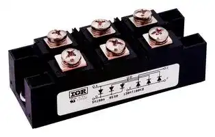


VS-90MT160KPBF
Bridge Rectifier, Three Phase, 1.6 kV, 90 A, Module, 6 Pins, 1.65 V
- Manufacturer: VISHAY
- Product type: Bridge Rectifier Diodes
- No. of Phases:Three Phase; Repetitive Reverse Voltage Vrrm Max:1.6kV; Forward Current If(AV):90A; Bridge Rectifier Case Style:Module; Forward Voltage VF Max:1.65V; No. of Pins:6Pins;
- SVHC: No SVHC (17-Dec-2014)
- No. of Pins: 6Pins
- No. of Phases: Three Phase
- Product Range: -
- Forward Voltage Max: 1.65V
- Forward Surge Current: 810A
- Average Forward Current: 90A
- Bridge Rectifier Mounting: Panel Mount
- Operating Temperature Max: 150°C
- Bridge Rectifier Case Style: Module
- Repetitive Peak Reverse Voltage: 1.6kV
| Delivery and price | |
|---|---|
| Units per pack | 15 |
| Price | 51.93 € |
| Current stock | 10+ |
| Lead time | 30 days |
**VS-90-110MT.KPbF Series** www.vishay.com ## Vishay Semiconductors ## **Three Phase Bridge (Power Modules), 90 A/110 A** ## **FEATURES** - Package fully compatible with the industry standard INT-A-PAK power modules series - High thermal conductivity package, electrically insulated case - Excellent power volume ratio, outline for easy connections to power transistor and IGBT modules **==> picture [18 x 6] intentionally omitted <==** **----- Start of picture text -----**<br> MTK<br>**----- End of picture text -----**<br> - 4000 VRMS isolating voltage - • UL E78996 approved - - Designed and qualified for industrial level - Material categorization: for definitions of compliance please see www.vishay.com/doc?99912 **PRIMARY CHARACTERISTICS DESCRIPTION** IO 90 A to 110 A A range of extremely compact, encapsulated three phase VRRM 800 V to 1600 V bridge rectifiers offering efficient and reliable operation. Package MTK They are intended for use in general purpose and heavy duty Circuit configuration Three phase bridge applications. **MAJOR RATINGS AND CHARACTERISTICS VALUES VALUES SYMBOL CHARACTERISTICS UNITS 90MT.K 110MT.K** 90 (120) 110 (150) A IO TC 90 (61) 90 (57) °C ~~|ee~~ 50 Hz 770 950 IFSM A 60 Hz 810 1000 ~~pfee~~ 50 Hz 3000 4500 I[2] t A[2] s 60 Hz 2700 4100 ~~|ee| GG~~ I[2] t 30 000 45 000 A[2] s ~~eG~~ VRRM Range 800 to 1600 V TStg Range -40 to 150 °C TJ -40 to 150 ~~==S=5Pp |pe |~~ **ELECTRICAL SPECIFICATIONS VOLTAGE RATINGS** A range of extremely compact, encapsulated three phase bridge rectifiers offering efficient and reliable operation. They are intended for use in general purpose and heavy duty |**VOLTAGE RATINGS**|**VOLTAGE RATINGS**|**VOLTAGE RATINGS**|**VOLTAGE RATINGS**|**VOLTAGE RATINGS**| |---|---|---|---|---| |**TYPE NUMBER**|**VOLTAGE**<br>**CODE**|**VRRM, MAXIMUM**<br>**REPETITIVE PEAK**<br>**REVERSE VOLTAGE**<br>**V**|**VRSM, MAXIMUM**<br>**NON-REPETITIVE PEAK**<br>**REVERSE VOLTAGE**<br>**V**|**IRRM MAXIMUM**<br>**AT TJ = MAXIMUM**<br>**mA**| |VS-90MT..K<br>VS-110MT..K|80|800|900|10| ||100|1000|1100|| ||120|1200|1300|| ||140|1400|1500|| ||160|1600|1700|| Revision: 17-Aug-17 Document Number: 94352 **1** For technical questions within your region: DiodesAmericas@vishay.com, DiodesAsia@vishay.com, DiodesEurope@vishay.com THIS DOCUMENT IS SUBJECT TO CHANGE WITHOUT NOTICE. THE PRODUCTS DESCRIBED HEREIN AND THIS DOCUMENT ARE SUBJECT TO SPECIFIC DISCLAIMERS, SET FORTH AT www.vishay.com/doc?91000 **VS-90-110MT.KPbF Series** Vishay Semiconductors **==> picture [59 x 48] intentionally omitted <==** www.vishay.com |**FORWARD CONDUCTION**|**FORWARD CONDUCTION**||||||| |---|---|---|---|---|---|---|---| |**PARAMETER**|**SYMBOL**|**TEST CONDITIONS**|||**VALUES**<br>**90MT.K**|**VALUES**<br>**110MT.K**|**UNITS**| |Maximum DC output current at case<br>temperature|IO|120° rect. conduction angle|||90 (120)|110 (150)|A| ||||||90 (61)|90 (57)|°C| |Maximum peak, one-cycle<br>forward, non-repetitive surge current|IFSM|t = 10 ms|No voltage<br>reapplied|Initial<br>TJ= TJmaximum|770|950|A| |||t = 8.3 ms|||810|1000|| |||t = 10 ms|100 % VRRM<br>reapplied||650|800|| |||t = 8.3 ms|||680|840|| |Maximum I2t for fusing|I2t|t = 10 ms|No voltage<br>reapplied||3000|4500|A2s| |||t = 8.3 ms|||2700|4100|| |||t = 10 ms|100 % VRRM <br>reapplied||2100|3200|| |||t = 8.3 ms|||1900|2900|| |Maximum I2t for fusing|I2t|t = 0.1 ms to 10 ms, no voltage reapplied|||30 000|45 000|A2s| |Low level value of<br>threshold voltage|VF(TO)1|(16.7 % xx IF(AV)< I <x IF(AV)), TJmaximum|||0.89|0.81|V| |High level value of threshold voltage|VF(TO)2|(I >x IF(AV)), TJmaximum|||1.05|0.99|| |Low level value of forward<br>slope resistance|rf1|(16.7 % xx IF(AV)< I <x IF(AV)), TJmaximum|||5.11|4.37|m| |High level value of forward<br>slope resistance|rf2|(I >x IF(AV)), TJmaximum|||4.64||| |Maximum forward voltage drop|VFM|Ipk= 150 A, TJ= 25 °C<br>tp= 400 μs single junction|||1.6|1.4|V| |RMS isolation voltage|VISOL|TJ= 25 °C, all terminal shorted<br>f = 50 Hz, t = 1 s|||4000||| ## **THERMAL AND MECHANICAL SPECIFICATIONS** |**THERMAL AND MECHANICAL SPECIFICATIONS**|**THERMAL AND MECHANICAL SPECIFICATIONS**|**THERMAL AND MECHANICAL SPECIFICATIONS**|**THERMAL AND MECHANICAL SPECIFICATIONS**|**THERMAL AND MECHANICAL SPECIFICATIONS**|**THERMAL AND MECHANICAL SPECIFICATIONS**|**THERMAL AND MECHANICAL SPECIFICATIONS**| |---|---|---|---|---|---|---| |**PARAMETER**||**SYMBOL**|**TEST CONDITIONS**|**VALUES**<br>**90MT.K**|**VALUES**<br>**110MT.K**|**UNITS**| |Maximum junction operating and<br>storage temperature range||TJ, TStg||-40 to 150||°C| |Maximum thermal resistance,<br>junction to case||RthJC|DC operation per module|0.21|0.18|°C/W| ||||DC operation per junction|1.26|1.07|| ||||120° rect. conduction angle per module|0.25|0.21|| ||||120° rect. conduction angle per junction|1.47|1.25|| |Maximum thermal resistance,<br>case to heatsink per module||RthCS|Mounting surface smooth, flat and greased|0.03||| |Mounting<br>torque ± 10 %|to heatsink||A mounting compound is recommended and the<br>torque should be rechecked after a period of<br>3 h to allow for the spread of the compound.<br>Lubricated threads.|4 to 6||Nm| ||to terminal|||3 to 4||| |Approximate weight||||176||g| Revision: 17-Aug-17 Document Number: 94352 **2** For technical questions within your region: DiodesAmericas@vishay.com, DiodesAsia@vishay.com, DiodesEurope@vishay.com THIS DOCUMENT IS SUBJECT TO CHANGE WITHOUT NOTICE. THE PRODUCTS DESCRIBED HEREIN AND THIS DOCUMENT ARE SUBJECT TO SPECIFIC DISCLAIMERS, SET FORTH AT www.vishay.com/doc?91000 **VS-90-110MT.KPbF Series** **==> picture [59 x 48] intentionally omitted <==** www.vishay.com ## Vishay Semiconductors **==> picture [204 x 368] intentionally omitted <==** **----- Start of picture text -----**<br> 150<br>90MT..K Series<br>140<br>130<br>120<br>120°<br>110<br>(Rect)<br>100<br>90<br>80 +<br>~<br>70 -<br>60<br>50<br>0 25 50 75 100 125<br>Total Output Current (A)<br>Fig. 1 - Current Ratings Characteristics<br>400<br>350<br>90MT..K Series<br>300 T J = 150 °C<br>250<br>120°<br>200 (Rect.)<br>150<br>100<br>50<br>0<br>0 20 40 60 80 100 120<br>Total Output Current (A)<br>Temperature (°C)<br>Maximum Allowable Case<br>Maximum Total Power Loss (W)<br>**----- End of picture text -----**<br> **==> picture [200 x 166] intentionally omitted <==** **----- Start of picture text -----**<br> 1000<br>100<br>TJ = 25 °C<br>TJ = 150 °C<br>10<br>90MT..K Series<br>Per junction<br>1<br>0 1 2 3 4 5<br>Instantaneous Forward Voltage (V)<br>Instantaneous Forward Current (A)<br>**----- End of picture text -----**<br> Fig. 2 - Forward Voltage Drop Characteristics **==> picture [204 x 175] intentionally omitted <==** **----- Start of picture text -----**<br> 400<br>350<br>300<br>250<br>200<br>150<br>100<br>50<br>0<br>0 25 50 75 100 125 150<br>Maximum Allowable Ambient<br>Temperature (°C)<br>1.5 K/W<br>1.0 K/W<br>0.7 K/W<br>0.05 K/W<br>0.3 K/W<br>0.2 K/W<br>0.12 K/WR<br>thSA<br> = 0.05 K/W - ΔR<br>Maximum Total Power Loss (W)<br>**----- End of picture text -----**<br> Fig. 3 - Total Power Loss Characteristics **==> picture [206 x 188] intentionally omitted <==** **----- Start of picture text -----**<br> 700<br>At any rated load condition and with<br>650 rated V RRM applied following surge.<br>600 Initial TJ = 150 °C<br>at 60 Hz 0.0083 s<br>550 at 50 Hz 0.0100 s<br>500<br>450<br>400<br>350<br>300<br>250 90MT..K Series<br>200<br>1 10 100<br>Number of Equal Amplitude Half<br>Cycle Current Pulses (N)<br>Fig. 4 - Maximum Non-Repetitive Surge Current<br>Peak Half Sine Wave Forward Current (A)<br>**----- End of picture text -----**<br> **==> picture [202 x 166] intentionally omitted <==** **----- Start of picture text -----**<br> 800<br>Maximum non-repetitive surge current<br>750 versus pulse train duration.<br>700 Initial T J = 150 °C<br>650 No voltage reapplied<br>Rated V RRM reapplied<br>600<br>500<br>450<br>400<br>350<br>300<br>250<br>90MT..K Series<br>200<br>150<br>0.01 0.1 1.0<br>Pulse Train Duration (s)<br>Peal Half Sine Wave Forward Current (A)<br>**----- End of picture text -----**<br> Fig. 5 - Maximum Non-Repetitive Surge Current Revision: 17-Aug-17 Document Number: 94352 **3** For technical questions within your region: DiodesAmericas@vishay.com, DiodesAsia@vishay.com, DiodesEurope@vishay.com THIS DOCUMENT IS SUBJECT TO CHANGE WITHOUT NOTICE. THE PRODUCTS DESCRIBED HEREIN AND THIS DOCUMENT ARE SUBJECT TO SPECIFIC DISCLAIMERS, SET FORTH AT www.vishay.com/doc?91000 **VS-90-110MT.KPbF Series** www.vishay.com **==> picture [59 x 48] intentionally omitted <==** ## Vishay Semiconductors **==> picture [204 x 166] intentionally omitted <==** **----- Start of picture text -----**<br> 150<br>110MT..K Series<br>140<br>130<br>120<br>110 120°<br>(Rect.)<br>100<br>90<br>80<br>+<br>70 ~<br>60 -<br>50<br>0 20 40 60 80 100 120 140 160<br>Total Output Current (A)<br>Temperature (°C)<br>Maximum Allowable Case<br>**----- End of picture text -----**<br> Fig. 6 - Current Ratings Characteristics **==> picture [200 x 166] intentionally omitted <==** **----- Start of picture text -----**<br> 1000<br>100<br>T J = 25 °C<br>TJ = 150 °C<br>10<br>110MT..K Series<br>Per junction<br>1<br>0 1 2 3 4 5<br>Instantaneous Forward Voltage (V)<br>Instantaneous Forward Current (A)<br>**----- End of picture text -----**<br> Fig. 7 - Forward Voltage Drop Characteristics **==> picture [500 x 399] intentionally omitted <==** **----- Start of picture text -----**<br> 450 450<br>110MT..K Series<br>400 400<br>TJ = 150 °C<br>350 350<br>300 300<br>120°<br>250 (Rect.) 250<br>200 200<br>150 150<br>100 100<br>50 50<br>0 0<br>0 25 50 75 100 125 150 0 25 50 75 100 125 150<br>Total Output Current (A) Maximum Allowable Ambient<br>Temperature (°C)<br>Fig. 8 - Total Power Loss Characteristics<br>900 1000<br>At any rated load condition and with Maximum non-repetitive surge current<br>800 rated VRRM applied following surge.Initial TJ = 150 °C 900 versus pulse train duration.Initial TJ = 150 °C<br>at 60 Hz 0.0083 s 800 No voltage reapplied<br>700 at 50 Hz 0.0100 s Rated VRRM reapplied<br>700<br>600<br>600<br>500<br>500<br>400<br>400<br>300 110MT..K Series 300 110MT..K Series<br>200 200<br>1 10 100 0.01 0.1 1<br>Number of Equal Amplitude Half Pulse Train Duration (s)<br>Cycle Current Pulses (N)<br>Fig. 9 - Maximum Non-Repetitive Surge Current Fig. 10 - Maximum Non-Repetitive Surge Current<br>1.5 K/W<br>1.0 K/W<br>0.7 K/W<br>0.4 K/W<br>0.5 K/W<br>0.3 K/W<br>0.2 K/W<br>0.12 K/W<br>R<br>thSA<br> = 0.05 K/W - ΔR<br>Maximum Total Power Loss (W) Maximum Total Power Loss (W)<br>Peak Half Sine Wave Forward Current (A) Peak Half Sine Wave Forward Current (A)<br>**----- End of picture text -----**<br> Revision: 17-Aug-17 Document Number: 94352 **4** For technical questions within your region: DiodesAmericas@vishay.com, DiodesAsia@vishay.com, DiodesEurope@vishay.com THIS DOCUMENT IS SUBJECT TO CHANGE WITHOUT NOTICE. THE PRODUCTS DESCRIBED HEREIN AND THIS DOCUMENT ARE SUBJECT TO SPECIFIC DISCLAIMERS, SET FORTH AT www.vishay.com/doc?91000 **VS-90-110MT.KPbF Series** **==> picture [59 x 48] intentionally omitted <==** www.vishay.com ## Vishay Semiconductors **==> picture [408 x 164] intentionally omitted <==** **----- Start of picture text -----**<br> 10<br>Steady state value<br>R thJC = 1.26 K/W<br>RthJC = 1.07 K/W 90MT..K Series<br>(DC operation)<br>1<br>110MT..K Series<br>0.1<br>Per junction<br>0.01<br>0.001 0.01 0.1 1 10<br>Square Wave Pulse Duration (s)<br> - Transient Thermal<br>Impedance (°C/W)<br>thJC<br>Z<br>**----- End of picture text -----**<br> Fig. 11 - Thermal Impedance ZthJC Characteristic ## **ORDERING INFORMATION TABLE** |**Device code**|**VS-**|**VS-**||**K**<br>**160**<br>**MT**<br>**0**<br>**11**|**K**<br>**160**<br>**MT**<br>**0**<br>**11**|**PbF**|**PbF**|| |---|---|---|---|---|---|---|---|---| |||||||||| |||||||||| ||1|||2<br>3<br>4<br>5||6||| ||**1**||-||Vishay Semiconductors product|||| ||**2**||-||Current rating code: 9 = 90 A (average)|||| ||||||11 = 110|A (average)||| ||**3**||-||Three phase diodes bridge|||| ||**4**||-||Essential part number|||| ||**5**||-||Voltage code x 10 = VRRM(see Voltage Ratings table)|||| ||**6**||-||PbF = Lead (Pb)-free|||| ## **Note** - To order the optional hardware go to www.vishay.com/doc?95172 ## **CIRCUIT CONFIGURATION** **==> picture [17 x 36] intentionally omitted <==** **----- Start of picture text -----**<br> A<br>B ~<br>C<br>**----- End of picture text -----**<br> **==> picture [94 x 98] intentionally omitted <==** **==> picture [15 x 112] intentionally omitted <==** **----- Start of picture text -----**<br> + D<br>E<br>-<br>F<br>**----- End of picture text -----**<br> ## **LINKS TO RELATED DOCUMENTS** Dimensions www.vishay.com/doc?95004 Revision: 17-Aug-17 **5** Document Number: 94352 For technical questions within your region: DiodesAmericas@vishay.com, DiodesAsia@vishay.com, DiodesEurope@vishay.com THIS DOCUMENT IS SUBJECT TO CHANGE WITHOUT NOTICE. THE PRODUCTS DESCRIBED HEREIN AND THIS DOCUMENT ARE SUBJECT TO SPECIFIC DISCLAIMERS, SET FORTH AT www.vishay.com/doc?91000 **Outline Dimensions** Vishay Semiconductors **==> picture [59 x 48] intentionally omitted <==** ## **MTK (with and without optional barrier)** ## **DIMENSIONS WITH OPTIONAL BARRIERS** in millimeters (inches) **==> picture [505 x 426] intentionally omitted <==** **----- Start of picture text -----**<br> Screws M5 x 0.8 length 10 Fast-on tab 2.8 x 0.8 (type 110) 24 ± 0.5<br>(0.94 ± 0.02)<br>35 ± 0.3<br>(1.38 ± 0.01)<br>5 ± 0.3 75 ± 0.5<br>(0.2 ± 0.01) (2.95 ± 0.02)<br>A B C<br>1 2 5 6<br>3 4 7 8<br>D E F<br>46 ± 0.3<br>(1.81 ± 0.01)<br>80 ± 0.3<br>(3.15 ± 0.01)<br>94 ± 0.3<br>(3.7 ± 0.01)<br>38 ± 0.5<br>(1.5 ± 0.02)<br>28 ± 1 30 ± 0.5<br>(1.11 ± 0.04) 25.5 ± 0.5 (1.004 ± 0.02) (1.17 ± 0.02)<br>8.5 ± 0.5<br>(0.34 ± 0.02)<br>14 ± 0.3 18 ± 0.3<br>(0.55 ± 0.01) (0.71 ± 0.01)<br>Ø 6.5 ± 0.2<br>(Ø 0.26 ± 0.01)<br>**----- End of picture text -----**<br> For technical questions, contact: indmodules@vishay.com www.vishay.com 1 Document Number: 95004 Revision: 27-Aug-07 ## **Outline Dimensions** ## Vishay Semiconductors MTK (with and without optional barrier) **==> picture [59 x 48] intentionally omitted <==** ## **DIMENSIONS WITHOUT OPTIONAL BARRIERS** in millimeters (inches) **==> picture [498 x 425] intentionally omitted <==** **----- Start of picture text -----**<br> Screws M5 x 0.8 length 10 Fast-on tab 2.8 x 0.8 (type 110)<br>24 ± 0.5<br>(0.94 ± 0.02)<br>35 ± 0.3<br>(1.38 ± 0.01)<br>5 ± 0.3 75 ± 0.5<br>(0.2 ± 0.01) (2.95 ± 0.02)<br>A B C<br>1 2 5 6<br>3 4 7 8<br>D E F<br>46 ± 0.3<br>(1.81 ± 0.01)<br>80 ± 0.3<br>(3.15 ± 0.01)<br>94 ± 0.3<br>(3.7 ± 0.01)<br>28 ± 1 30 ± 0.5<br>(1.11 ± 0.04) 25.5 ± 0.5 (1.004 ± 0.02) (1.17 ± 0.02)<br>8.5 ± 0.5<br>(0.34 ± 0.02)<br>14 ± 0.3 18 ± 0.3<br>(0.55 ± 0.01) (0.71 ± 0.01)<br>Ø 6.5 ± 0.2<br>(Ø 0.26 ± 0.01)<br>**----- End of picture text -----**<br> For technical questions, contact: indmodules@vishay.com Document Number: 95004 Revision: 27-Aug-07 www.vishay.com 2 **Legal Disclaimer Notice** Vishay www.vishay.com **==> picture [59 x 48] intentionally omitted <==** ## **Disclaimer** ALL PRODUCT, PRODUCT SPECIFICATIONS AND DATA ARE SUBJECT TO CHANGE WITHOUT NOTICE TO IMPROVE RELIABILITY, FUNCTION OR DESIGN OR OTHERWISE. Vishay Intertechnology, Inc., its affiliates, agents, and employees, and all persons acting on its or their behalf (collectively, “Vishay”), disclaim any and all liability for any errors, inaccuracies or incompleteness contained in any datasheet or in any other disclosure relating to any product. Vishay makes no warranty, representation or guarantee regarding the suitability of the products for any particular purpose or the continuing production of any product. To the maximum extent permitted by applicable law, Vishay disclaims (i) any and all liability arising out of the application or use of any product, (ii) any and all liability, including without limitation special, consequential or incidental damages, and (iii) any and all implied warranties, including warranties of fitness for particular purpose, non-infringement and merchantability. Statements regarding the suitability of products for certain types of applications are based on Vishay’s knowledge of typical requirements that are often placed on Vishay products in generic applications. Such statements are not binding statements about the suitability of products for a particular application. It is the customer’s responsibility to validate that a particular product with the properties described in the product specification is suitable for use in a particular application. Parameters provided in datasheets and / or specifications may vary in different applications and performance may vary over time. All operating parameters, including typical parameters, must be validated for each customer application by the customer’s technical experts. Product specifications do not expand or otherwise modify Vishay’s terms and conditions of purchase, including but not limited to the warranty expressed therein. Except as expressly indicated in writing, Vishay products are not designed for use in medical, life-saving, or life-sustaining applications or for any other application in which the failure of the Vishay product could result in personal injury or death. Customers using or selling Vishay products not expressly indicated for use in such applications do so at their own risk. Please contact authorized Vishay personnel to obtain written terms and conditions regarding products designed for such applications. No license, express or implied, by estoppel or otherwise, to any intellectual property rights is granted by this document or by any conduct of Vishay. Product names and markings noted herein may be trademarks of their respective owners. _**© 2017 VISHAY INTERTECHNOLOGY, INC. ALL RIGHTS RESERVED**_ Revision: 08-Feb-17 Document Number: 91000 **1**
Updated at June 4, 2026
Vishay is a global leader in the manufacturing of discrete semiconductors and passive electronic components. Renowned for its exceptional quality and engineering expertise, the company produces highly reliable solutions that drive innovation across the industrial, automotive, telecommunications, and consumer electronics markets. From advanced factory automation to vehicle electrification, Vishay components provide the foundational building blocks for modern electronic design. The company's expansive portfolio is heavily focused on efficient power management, signal routing, and energy storage. Within its passive component lineup, Vishay is recognized for its extensive array of high-performance capacitors, including robust aluminium electrolytic, film, and polymer variants, alongside highly efficient power inductors. In the realm of discrete semiconductors, Vishay is a premier manufacturer of single and dual MOSFETs, as well as a vast selection of Schottky, Zener, and fast-recovery rectifier diodes designed for demanding power applications. Furthermore, Vishay delivers industry-leading circuit protection and thermal management solutions. With a broad offering of transient voltage suppressors (TVS diodes) and temperature-sensing NTC thermistors, these components are engineered to safeguard sensitive circuitry against both electrical and thermal overstress. By combining this vital mix of advanced discretes and passives, Vishay enables engineers to develop robust, space-saving, and highly resilient electronic systems.
About Novapart
Novapart is a B2B electronic component broker specialising in stock shortages and cost reduction. We source hard-to-find parts and identify compliant alternatives across a catalogue of 540,000+ components from 500+ manufacturers.
Learn more →Stock Shortage Specialist
When a component is unavailable, discontinued or has an unacceptable lead time, we tap into our network of vetted European and Asian distributors to source what you need — without compromising on quality or traceability.
Request a quote →Compliant Alternatives
We identify pin-to-pin, electrically equivalent substitutes that meet the same certifications (RoHS, AEC-Q100, REACH) as your original specification — validated against datasheets, not just part numbers. Often at a lower cost.
BOM Analysis service →