


VS-8DKH02HM3/H
Fast / Ultrafast Diode, 200 V, 8 A, Dual Isolated, 960 mV, 25 ns, 173 A
- Manufacturer: VISHAY
- Product type: Fast & Ultrafast Recovery Rectifier Diodes
- Repetitive Reverse Voltage Vrrm Max:200V; Forward Current If(AV):8A; Diode Configuration:Dual Isolated; Forward Voltage VF Max:960mV; Reverse Recovery Time trr Max:25ns; Forward Su
- SVHC: Lead (04-Feb-2026)
- No. of Pins: 8 Pin
- Product Range: -
- Qualification: AEC-Q101
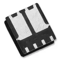
- Diode Case Style: FlatPAK
- Diode Configuration: Dual Isolated
- Forward Voltage Max: 960mV
- Forward Surge Current: 173A
- Reverse Recovery Time: 25ns
- Average Forward Current: 8A
- Operating Temperature Max: 175°C
- Repetitive Peak Reverse Voltage: 200V
| Delivery and price | |
|---|---|
| Units per pack | 1500 |
| Price | 0.273 € |
| Current stock | 10+ |
| Lead time | 30 days |
**VS-8DKH02HM3** www.vishay.com ## Vishay Semiconductors ## **Hyperfast Rectifier, 2 x 4 A FRED Pt[®]** **==> picture [118 x 82] intentionally omitted <==** **----- Start of picture text -----**<br> 1<br>2<br>3<br>4<br>8<br>7<br>6<br>5<br>**----- End of picture text -----**<br> ## **FEATURES** - Hyperfast recovery time, reduced Qrr, and soft recovery - 175 °C maximum operating junction temperature - Specific for output and snubber operation - Low forward voltage drop - Low leakage current **==> picture [81 x 40] intentionally omitted <==** **----- Start of picture text -----**<br> FlatPAK 5 x 6<br>1, 2 Ow 7, 8<br>3, 4 O— > 5, 6<br>**----- End of picture text -----**<br> - AEC-Q101 qualified - Meets MSL level 1 per J-STD-020, LF maximum peak of 260 °C - Material categorization: for definitions of compliance please see www.vishay.com/doc?99912 ## **LINKS TO ADDITIONAL RESOURCES** ~~a~~ 3D Models |**PRIMARY CHARACTERISTICS**|**PRIMARY CHARACTERISTICS**| |---|---| |IF(AV)|2 x 4 A| |VR|200 V| |VFat IF|0.7 V| |trr(typ.)|25 ns| |TJmax.|175 °C| |Package|FlatPAK 5 x 6| |Circuit configuration|Separated cathode| ## **DESCRIPTION / APPLICATIONS** State of the art hyperfast recovery rectifiers specifically designed with optimized performance of forward voltage drop and hyperfast recovery time. The planar structure and the platinum doped life time control guarantee the best overall performance, ruggedness, and reliability characteristics. These devices are intended for use in snubber, boost, piezo-injection, as high frequency rectifiers, and freewheeling diodes. The extremely optimized stored charge and low recovery current minimize the switching losses and reduce power dissipation in the switching element. ## **MECHANICAL DATA** **Case:** FlatPAK 5 x 6 Molding compound meets UL 94 V-0 flammability rating Halogen-free, RoHS-compliant **Terminals:** matte tin plated leads, solderable per J-STD-002, meets JESD 201 class 2 whisker test ## **ABSOLUTE MAXIMUM RATINGS** |**ABSOLUTE MAXIMUM RATINGS**|**ABSOLUTE MAXIMUM RATINGS**|**ABSOLUTE MAXIMUM RATINGS**|**ABSOLUTE MAXIMUM RATINGS**|**ABSOLUTE MAXIMUM RATINGS**| |---|---|---|---|---| |**PARAMETER**|**SYMBOL**|**TEST CONDITIONS**|**VALUES**|**UNITS**| |Peak repetitive reverse voltage|VRRM||200|V| |Average rectified forward current<br>per device|IF(AV)|TSolderpad= 170 °C, DC|8|A| |||TSolderpad= 169 °C, D = 0.5||| |Non-repetitive peak surge current<br>per device<br>per diode|IFSM|TJ= 25 °C, 10 ms sinusoidal pulse|173|| ||||87|| |Operatingjunction and storage temperatures|TJ, TStg||-55 to +175|°C| ## **ELECTRICAL SPECIFICATIONS** (TJ = 25 °C unless otherwise specified) |**ELECTRICAL SPECIFICATIONS**(TJ = 25 °C unless otherwise specified)TJ = 25 °C unless otherwise specified)J = 25 °C unless otherwise specified)= 25 °C unless otherwise specified)pecified)ecified))|**ELECTRICAL SPECIFICATIONS**(TJ = 25 °C unless otherwise specified)TJ = 25 °C unless otherwise specified)J = 25 °C unless otherwise specified)= 25 °C unless otherwise specified)pecified)ecified))|**ELECTRICAL SPECIFICATIONS**(TJ = 25 °C unless otherwise specified)TJ = 25 °C unless otherwise specified)J = 25 °C unless otherwise specified)= 25 °C unless otherwise specified)pecified)ecified))|**ELECTRICAL SPECIFICATIONS**(TJ = 25 °C unless otherwise specified)TJ = 25 °C unless otherwise specified)J = 25 °C unless otherwise specified)= 25 °C unless otherwise specified)pecified)ecified))|**ELECTRICAL SPECIFICATIONS**(TJ = 25 °C unless otherwise specified)TJ = 25 °C unless otherwise specified)J = 25 °C unless otherwise specified)= 25 °C unless otherwise specified)pecified)ecified))|**ELECTRICAL SPECIFICATIONS**(TJ = 25 °C unless otherwise specified)TJ = 25 °C unless otherwise specified)J = 25 °C unless otherwise specified)= 25 °C unless otherwise specified)pecified)ecified))|**ELECTRICAL SPECIFICATIONS**(TJ = 25 °C unless otherwise specified)TJ = 25 °C unless otherwise specified)J = 25 °C unless otherwise specified)= 25 °C unless otherwise specified)pecified)ecified))| |---|---|---|---|---|---|---| |**PARAMETER**|**SYMBOL**|**TEST CONDITIONS**|**MIN.**|**TYP.**|**MAX.**|**UNITS**| |Breakdown voltage, blockingvoltage|VBR, VR|IR= 100 μA|200|-|-|V| |Forward voltage, per diode|VF|IF= 4 A|-|0.87|0.96|| |||IF= 4 A, TJ= 150 °C|-|0.7|0.78|| |Reverse leakage current, per diode|IR|VR= VRrated|-|-|2|μA| |||TJ= 150 °C, VR= VRrated|-|7|80|| |Junction capacitance|CT|VR= 200 V|-|19|-|pF| Revision: 29-Jan-2021 **1** Document Number: 96088 For technical questions within your region: DiodesAmericas@vishay.com, DiodesAsia@vishay.com, DiodesEurope@vishay.com THIS DOCUMENT IS SUBJECT TO CHANGE WITHOUT NOTICE. THE PRODUCTS DESCRIBED HEREIN AND THIS DOCUMENT ARE SUBJECT TO SPECIFIC DISCLAIMERS, SET FORTH AT www.vishay.com/doc?91000 **VS-8DKH02HM3** Vishay Semiconductors www.vishay.com |**DYNAMIC RECOVERY CHARACTERISTICS**(TJ= 25 °C unless otherwise specified)|**DYNAMIC RECOVERY CHARACTERISTICS**(TJ= 25 °C unless otherwise specified)|**DYNAMIC RECOVERY CHARACTERISTICS**(TJ= 25 °C unless otherwise specified)|**DYNAMIC RECOVERY CHARACTERISTICS**(TJ= 25 °C unless otherwise specified)|**DYNAMIC RECOVERY CHARACTERISTICS**(TJ= 25 °C unless otherwise specified)|**DYNAMIC RECOVERY CHARACTERISTICS**(TJ= 25 °C unless otherwise specified)|**DYNAMIC RECOVERY CHARACTERISTICS**(TJ= 25 °C unless otherwise specified)|**DYNAMIC RECOVERY CHARACTERISTICS**(TJ= 25 °C unless otherwise specified)| |---|---|---|---|---|---|---|---| |**PARAMETER**|**SYMBOL**|**TEST CONDITIONS**||**MIN.**|**TYP.**|**MAX.**|**UNITS**| |Reverse recovery time|trr|IF= 1.0 A, dIF/dt = 50 A/μs, VR= 30 V||-|20|-|ns| |||IF= 0.5 A, IR= 1 A, Irr= 0.25 A||-|-|25|| |||TJ= 25 °C|IF= 4 A<br>dIF/dt = 200 A/μs<br>VR= 160 V|-|17|-|| |||TJ= 125 °C||-|29|-|| |Peak recovery current|IRRM|TJ= 25 °C||-|2.1|-|A| |||TJ= 125 °C||-|4|-|| |Reverse recovery charge|Qrr|TJ= 25 °C||-|18|-|nC| |||TJ= 125 °C||-|60|-|| |**THERMAL - MECHANICAL SPECIFICATIONS**|**THERMAL - MECHANICAL SPECIFICATIONS**|**THERMAL - MECHANICAL SPECIFICATIONS**|**THERMAL - MECHANICAL SPECIFICATIONS**|**THERMAL - MECHANICAL SPECIFICATIONS**|**THERMAL - MECHANICAL SPECIFICATIONS**|**THERMAL - MECHANICAL SPECIFICATIONS**| |---|---|---|---|---|---|---| |**PARAMETER**|**SYMBOL**|**TEST CONDITIONS**|**MIN.**|**TYP.**|**MAX.**|**UNITS**| |Maximum junction and storage temperature range|TJ, TStg||-55|-|175|°C| |Thermal resistance, junction to ambient, per diode|RthJA (1)(2)||-|89|103|°C/W| |Thermal resistance, junction to mount, per diode|RthJM (3)||-|1.8|2.1|| ## **Notes** > (1) The heat generated must be less than the thermal conductivity from junction to ambient: dPD/dTJ < 1/ RthJA > (2) Free air, mounted or recommended copper pad area; thermal resistance RthJA - junction to ambient > (3) Mounted on infinite heatsink Revision: 29-Jan-2021 Document Number: 96088 **2** For technical questions within your region: DiodesAmericas@vishay.com, DiodesAsia@vishay.com, DiodesEurope@vishay.com THIS DOCUMENT IS SUBJECT TO CHANGE WITHOUT NOTICE. THE PRODUCTS DESCRIBED HEREIN AND THIS DOCUMENT ARE SUBJECT TO SPECIFIC DISCLAIMERS, SET FORTH AT www.vishay.com/doc?91000 **VS-8DKH02HM3** www.vishay.com ## Vishay Semiconductors **==> picture [202 x 164] intentionally omitted <==** **----- Start of picture text -----**<br> 100<br>T J = 175 °C<br>10 TJ = 150 °C<br>TJ = 125 °C<br>1<br>T J = 25 °C<br>TJ = -40 °C<br>0.1<br>0.1 0.3 0.5 0.7 0.9 1.1 1.3 1.5<br>VF - Forward Voltage Drop (V)<br> - Instantaneous Forward Current (A)<br>IF<br>**----- End of picture text -----**<br> Fig. 1 - Typical Forward Voltage Drop Characteristics **==> picture [204 x 165] intentionally omitted <==** **----- Start of picture text -----**<br> 100<br>TJ = 175 °C<br>10 TJ = 150 °C<br>1<br>TJ = 125 °C<br>0.1<br>0.01<br>TJ = 25 °C<br>0.001<br>0.0001<br>0 50 100 150 200<br>VR - Reverse Voltage (V)<br> - Reverse Current (µA)<br>IR<br>**----- End of picture text -----**<br> Fig. 2 - Typical Values of Reverse Current vs. Reverse Voltage **==> picture [203 x 165] intentionally omitted <==** **----- Start of picture text -----**<br> 100<br>10<br>0 50 100 150 200<br>VR - Reverse Voltage (V)<br> - Junction Capacitance (pF)<br>T<br>C<br>**----- End of picture text -----**<br> Fig. 3 - Typical Junction Capacitance vs. Reverse Voltage **==> picture [409 x 163] intentionally omitted <==** **----- Start of picture text -----**<br> 1000<br>100 Junction to ambient<br>10<br>Junction to case<br>1<br>0.1<br>0.01<br>0.00001 0.0001 0.001 0.01 0.1 1 10 100 1000<br>t1 - Rectangular Pulse Duration (s)<br>C/W)<br>°<br> - Thermal Impedance (<br>th<br>Z<br>**----- End of picture text -----**<br> Fig. 4 - Maximum Thermal Impedance ZthJC Characteristics Revision: 29-Jan-2021 Document Number: 96088 **3** For technical questions within your region: DiodesAmericas@vishay.com, DiodesAsia@vishay.com, DiodesEurope@vishay.com THIS DOCUMENT IS SUBJECT TO CHANGE WITHOUT NOTICE. THE PRODUCTS DESCRIBED HEREIN AND THIS DOCUMENT ARE SUBJECT TO SPECIFIC DISCLAIMERS, SET FORTH AT www.vishay.com/doc?91000 **VS-8DKH02HM3** www.vishay.com ## Vishay Semiconductors **==> picture [196 x 149] intentionally omitted <==** **----- Start of picture text -----**<br> 200<br>180<br>160<br>Tc = 170 °C<br>140 R thJC = 1.8 °C/W<br>120<br>100<br>80<br>60<br>40 T c = 28 °C<br>RthJA = 89 °C/W<br>20<br>0<br>0 0.5 1 1.5 2 2.5 3 3.5 4 4.5 5<br>C)<br>°<br>Allowable Case Temperature (<br>**----- End of picture text -----**<br> **==> picture [134 x 10] intentionally omitted <==** **----- Start of picture text -----**<br> IF(AV) - Average Forward Current (A)<br>**----- End of picture text -----**<br> Fig. 5 - Maximum Allowable Case Temperature vs. Average Forward Current **==> picture [203 x 149] intentionally omitted <==** **----- Start of picture text -----**<br> 40<br>35<br>30<br>125 °C<br>25<br>20<br>25 °C<br>15<br>10<br>5<br>100 1000<br> (ns)<br>trr<br>**----- End of picture text -----**<br> **==> picture [47 x 9] intentionally omitted <==** **----- Start of picture text -----**<br> dIF/dt (A/µs)<br>**----- End of picture text -----**<br> Fig. 7 - Typical Reverse Recovery Time vs. dIF/dt **==> picture [199 x 148] intentionally omitted <==** **----- Start of picture text -----**<br> 5<br>4.5<br>RMS limit<br>4<br>3.5<br>3<br>2.5<br>D = 0.01<br>2 D = 0.05<br>D = 0.1<br>1.5 D = 0.2<br>D = 0.5<br>1 DC<br>0.5<br>0<br>0 1 2 3 4 5 6<br>Average Power Loss (W)<br>**----- End of picture text -----**<br> **==> picture [134 x 10] intentionally omitted <==** **----- Start of picture text -----**<br> IF(AV) - Average Forward Current (A)<br>**----- End of picture text -----**<br> Fig. 6 - Forward Power Loss Characteristics **==> picture [206 x 149] intentionally omitted <==** **----- Start of picture text -----**<br> 100<br>90<br>80<br>70 125 °C<br>60<br>50<br>40 25 ° C<br>30<br>20<br>10<br>0<br>100 1000<br> (nC)<br>rr<br>Q<br>**----- End of picture text -----**<br> **==> picture [47 x 9] intentionally omitted <==** **----- Start of picture text -----**<br> dIF/dt (A/µs)<br>**----- End of picture text -----**<br> Fig. 8 - Typical Stored Charge vs. dIF/dt **==> picture [271 x 221] intentionally omitted <==** **----- Start of picture text -----**<br> (3)<br>IF trr<br>ta tb<br>0<br>(4)<br>Qrr<br>(2)<br>IRRM 0.5 IRRM<br>di(rec)M/dt (5)<br>0.75 IRRM<br>(1) diF/dt<br>(1) diF/dt - rate of change of current (4) Qrr - area under curve defined by trr<br> through zero crossing and IRRM<br>(2) IRRM - peak reverse recovery current Qrr = t 2rr x IRRM<br> from zero crossing point of negative (3) trr - reverse recovery time measured (5) di(rec)M/dt - peak rate of change of<br> going IF to point where a line passing current during tb portion of trr<br> through 0.75 IRRM and 0.50 IRRM<br> extrapolated to zero current.<br>**----- End of picture text -----**<br> Fig. 9 - Reverse Recovery Waveform and Definitions **4** Revision: 29-Jan-2021 Document Number: 96088 For technical questions within your region: DiodesAmericas@vishay.com, DiodesAsia@vishay.com, DiodesEurope@vishay.com THIS DOCUMENT IS SUBJECT TO CHANGE WITHOUT NOTICE. THE PRODUCTS DESCRIBED HEREIN AND THIS DOCUMENT ARE SUBJECT TO SPECIFIC DISCLAIMERS, SET FORTH AT www.vishay.com/doc?91000 **VS-8DKH02HM3** www.vishay.com ## Vishay Semiconductors ## **ORDERING INFORMATION TABLE** |**Device code**|**VS-**|**VS-**||**8**<br>**D**<br>**K**<br>**H**|**8**<br>**D**<br>**K**<br>**H**|**02**|**H**|**M3**|| |---|---|---|---|---|---|---|---|---|---| |||1||5<br>3<br>2<br>4||6|7|8|| ||**1**||-||Vishay Semiconductors product||||| ||**2**||-||Current rating (8 = 8 A)||||| ||**3**||-||Circuit configuration:||||| ||||||D = separated cathode||||| ||**4**||-||K = FlatPAK package||||| ||**5**||-||Process type,||||| ||||||H = hyper fast recovery||||| ||**6**||-||Voltage code (02 = 200 V)||||| ||**7**||-||H = AEC-Q101 qualified||||| ||**8**||-||M3 = halogen-free, RoHS-compliant, and terminations lead (Pb)-free||||| ## **ORDERING INFORMATION** (example) |**ORDERING INFORMATION**(example)|**ORDERING INFORMATION**(example)|**ORDERING INFORMATION**(example)|**ORDERING INFORMATION**(example)|**ORDERING INFORMATION**(example)| |---|---|---|---|---| |**PREFERRED P/N**|**UNIT WEIGHT**<br>**(g)**|**PREFERRED PACKAGE CODE**|**BASE QUANTITY**|**PACKAGING DESCRIPTION**| |VS-8DKH02HM3/H|0.10|H|1500|7"diameter plastic tape and reel| |VS-8DKH02HM3/I|0.10|I|6000|13"diameter plastic tape and reel| |||| |---|---|---| |**LINKS TO RELATED DOCUMENTS**||| |Dimensions||www.vishay.com/doc?96056| |Part marking information||www.vishay.com/doc?96059| |Packaging information||www.vishay.com/doc?88869| Revision: 29-Jan-2021 Document Number: 96088 **5** For technical questions within your region: DiodesAmericas@vishay.com, DiodesAsia@vishay.com, DiodesEurope@vishay.com THIS DOCUMENT IS SUBJECT TO CHANGE WITHOUT NOTICE. THE PRODUCTS DESCRIBED HEREIN AND THIS DOCUMENT ARE SUBJECT TO SPECIFIC DISCLAIMERS, SET FORTH AT www.vishay.com/doc?91000 **Outline Dimensions** Vishay Semiconductors **==> picture [59 x 48] intentionally omitted <==** www.vishay.com ## **FlatPAK 5 x 6 (Dual)** ## **DIMENSIONS** in inches (millimeters) **==> picture [158 x 288] intentionally omitted <==** **----- Start of picture text -----**<br> D<br>D1<br>8 7 6 5<br>F2 F1<br>(2 x d2)<br>1 2 3 4<br>Top View<br>(8 x Θ)<br>Side View<br>E E1<br>(8 x a)<br>c<br>A<br>**----- End of picture text -----**<br> **==> picture [175 x 393] intentionally omitted <==** **----- Start of picture text -----**<br> 6 x e 8 x b<br>5 6 7 8<br>(d1)<br>F1 F2<br>4 3 2 1<br>D3<br>2 x D4<br>D2<br>Bottom View<br>0.180 (4.56)<br>0.030 (0.75) 0.082 (2.08)<br>0.219 (5.55)<br>0.050 (1.27)<br>0.030 (0.75)<br>PCB Footprint<br>4 x L2<br>M<br>(E3) 2 x b1 E2<br>)(K<br>4 x L1<br>0.055 (1.40)<br>0.191 (4.84) 0.022 (0.56)<br>0.259 (6.59)<br>0.039 (1.00)<br>**----- End of picture text -----**<br> |||||**PCB Footprint**<br>0.050 (1.27)<br>0.030 (0.75)<br>0.039 (1.00)|**PCB Footprint**<br>0.050 (1.27)<br>0.030 (0.75)<br>0.039 (1.00)|**PCB Footprint**<br>0.050 (1.27)<br>0.030 (0.75)<br>0.039 (1.00)| |---|---|---|---|---|---|---| |**DIM.**|**INCHES**|||**MILLIMETERS**||| ||**MIN.**|**NOM.**|**MAX.**|**MIN.**|**NOM.**|**MAX.**| |A|0.035|0.039|0.043|0.89|0.99|1.09| |(a)|-|0.006|-|-|0.15|-| |b|0.013|0.017|0.020|0.32|0.43|0.52| |b1|0.013|0.017|0.020|0.32|0.43|0.52| |c|0.008|-|0.014|0.20|-|0.35| |D|0.197|0.203|0.209|5.00|5.15|5.30| |D1|0.189|0.193|0.197|4.80|4.90|5.00| |D2|0.154|0.161|0.169|3.90|4.10|4.30| |D3|0.020|0.024|0.031|0.50|0.60|0.80| |D4|0.063|0.069|0.075|1.60|1.75|1.90| |(d1)|-|0.016|-|-|0.40|-| |(d2)|-|0.005|-|-|0.125|-| |E|0.238|0.244|0.250|6.05|6.20|6.35| Revision: 27-Mar-18 **1** Document Number: 96056 For technical questions within your region: DiodesAmericas@vishay.com, DiodesAsia@vishay.com, DiodesEurope@vishay.com THIS DOCUMENT IS SUBJECT TO CHANGE WITHOUT NOTICE. THE PRODUCTS DESCRIBED HEREIN AND THIS DOCUMENT ARE SUBJECT TO SPECIFIC DISCLAIMERS, SET FORTH AT www.vishay.com/doc?91000 **Outline Dimensions** Vishay Semiconductors **==> picture [59 x 48] intentionally omitted <==** www.vishay.com |**DIM.**|**INCHES**|**INCHES**|**INCHES**|**MILLIMETERS**|**MILLIMETERS**|**MILLIMETERS**| |---|---|---|---|---|---|---| ||**MIN.**|**NOM.**|**MAX.**|**MIN.**|**NOM.**|**MAX.**| |E1|0.228|0.232|0.236|5.80|5.90|6.00| |E2|0.157|0.165|0.173|4.00|4.20|4.40| |(E3)|-|0.144|-|-|3.65|-| |e|0.050 BSC|||1.27 BSC||| |(K)|0.039|-|-|1.00|-|-| |L1|0.019|-|0.043|0.48|-|1.10| |L2|0.012|-|0.031|0.30|-|0.80| |M|0.128|0.138|0.148|3.25|3.50|3.75| ||0°|-|10°|0°|-|10°| ## **Notes** - Dimensioning and tolerancing per ASME Y14.5-2009 - Dimensions D1 and E1 do not include mold flash or gate burrs - Dimension (XX) means reference only Revision: 27-Mar-18 Document Number: 96056 **2** For technical questions within your region: DiodesAmericas@vishay.com, DiodesAsia@vishay.com, DiodesEurope@vishay.com THIS DOCUMENT IS SUBJECT TO CHANGE WITHOUT NOTICE. THE PRODUCTS DESCRIBED HEREIN AND THIS DOCUMENT ARE SUBJECT TO SPECIFIC DISCLAIMERS, SET FORTH AT www.vishay.com/doc?91000 **Legal Disclaimer Notice** Vishay www.vishay.com ## **Disclaimer** ALL PRODUCT, PRODUCT SPECIFICATIONS AND DATA ARE SUBJECT TO CHANGE WITHOUT NOTICE TO IMPROVE RELIABILITY, FUNCTION OR DESIGN OR OTHERWISE. Vishay Intertechnology, Inc., its affiliates, agents, and employees, and all persons acting on its or their behalf (collectively, “Vishay”), disclaim any and all liability for any errors, inaccuracies or incompleteness contained in any datasheet or in any other disclosure relating to any product. Vishay makes no warranty, representation or guarantee regarding the suitability of the products for any particular purpose or the continuing production of any product. To the maximum extent permitted by applicable law, Vishay disclaims (i) any and all liability arising out of the application or use of any product, (ii) any and all liability, including without limitation special, consequential or incidental damages, and (iii) any and all implied warranties, including warranties of fitness for particular purpose, non-infringement and merchantability. Statements regarding the suitability of products for certain types of applications are based on Vishay’s knowledge of typical requirements that are often placed on Vishay products in generic applications. Such statements are not binding statements about the suitability of products for a particular application. It is the customer’s responsibility to validate that a particular product with the properties described in the product specification is suitable for use in a particular application. Parameters provided in datasheets and / or specifications may vary in different applications and performance may vary over time. All operating parameters, including typical parameters, must be validated for each customer application by the customer’s technical experts. Product specifications do not expand or otherwise modify Vishay’s terms and conditions of purchase, including but not limited to the warranty expressed therein. Except as expressly indicated in writing, Vishay products are not designed for use in medical, life-saving, or life-sustaining applications or for any other application in which the failure of the Vishay product could result in personal injury or death. Customers using or selling Vishay products not expressly indicated for use in such applications do so at their own risk. Please contact authorized Vishay personnel to obtain written terms and conditions regarding products designed for such applications. No license, express or implied, by estoppel or otherwise, to any intellectual property rights is granted by this document or by any conduct of Vishay. Product names and markings noted herein may be trademarks of their respective owners. _**© 2021 VISHAY INTERTECHNOLOGY, INC. ALL RIGHTS RESERVED**_ Revision: 01-Jan-2021 Document Number: 91000 **1**
Updated at June 4, 2026
Vishay is a global leader in the manufacturing of discrete semiconductors and passive electronic components. Renowned for its exceptional quality and engineering expertise, the company produces highly reliable solutions that drive innovation across the industrial, automotive, telecommunications, and consumer electronics markets. From advanced factory automation to vehicle electrification, Vishay components provide the foundational building blocks for modern electronic design. The company's expansive portfolio is heavily focused on efficient power management, signal routing, and energy storage. Within its passive component lineup, Vishay is recognized for its extensive array of high-performance capacitors, including robust aluminium electrolytic, film, and polymer variants, alongside highly efficient power inductors. In the realm of discrete semiconductors, Vishay is a premier manufacturer of single and dual MOSFETs, as well as a vast selection of Schottky, Zener, and fast-recovery rectifier diodes designed for demanding power applications. Furthermore, Vishay delivers industry-leading circuit protection and thermal management solutions. With a broad offering of transient voltage suppressors (TVS diodes) and temperature-sensing NTC thermistors, these components are engineered to safeguard sensitive circuitry against both electrical and thermal overstress. By combining this vital mix of advanced discretes and passives, Vishay enables engineers to develop robust, space-saving, and highly resilient electronic systems.
About Novapart
Novapart is a B2B electronic component broker specialising in stock shortages and cost reduction. We source hard-to-find parts and identify compliant alternatives across a catalogue of 410,000+ components from 500+ manufacturers.
Learn more →Stock Shortage Specialist
When a component is unavailable, discontinued or has an unacceptable lead time, we tap into our network of vetted European and Asian distributors to source what you need — without compromising on quality or traceability.
Request a quote →Compliant Alternatives
We identify pin-to-pin, electrically equivalent substitutes that meet the same certifications (RoHS, AEC-Q100, REACH) as your original specification — validated against datasheets, not just part numbers. Often at a lower cost.
BOM Analysis service →