


VS-110RKI120PBF
Thyristor Module, 110 A, 1200 V
- Manufacturer: VISHAY
- Product type: Thyristors - SCR Modules
- SCR Module Type: Single SCR
- Thyristor Mounting: Stud Mount
- Holding Current Max: 200mA
- On State RMS Current: 175A
- Thyristor Case Style: TO-209AC
- Average Forward Current: 110A
- Average On State Current: 110A
- Gate Trigger Current Max: 100mA
- Gate Trigger Voltage Max: 2.5V
- Operating Temperature Max: 140°C
- Repetitive Peak Reverse Voltage: 1.2kV
- Peak Repetitive Off State Voltage: 1.2kV
| Delivery and price | |
|---|---|
| Units per pack | 50 |
| Price | 31.96 € |
| Current stock | 10+ |
| Lead time | 30 days |
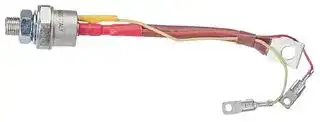
## **VS-110RKI...PbF, VS-111RKI...PbF Series** www.vishay.com ## Vishay Semiconductors ## **Phase Control Thyristors (Stud Version), 110 A** ## **FEATURES** - High current and high surge ratings - Hermetic ceramic housing - Designed and qualified for industrial level - Material categorization: For definitions of compliance please see www.vishay.com/doc?99912 **==> picture [70 x 9] intentionally omitted <==** **----- Start of picture text -----**<br> TO-209AC (TO-94)<br>**----- End of picture text -----**<br> ## **TYPICAL APPLICATIONS** - DC motor controls ## **PRODUCT SUMMARY** - Controlled DC power supplies - AC controllers |**PRODUCT SUMMARY**|**PRODUCT SUMMARY**| |---|---| |IT(AV)|110 A| |VDRM/VRRM|400 V, 800 V, 1200 V| |VTM|1.57 V| |IGT|80 mA| |TJ|-40 °C to 140 °C| |Package|TO-209AC (TO-94)| |Diode variation|Single SCR| ## **MAJOR RATINGS AND CHARACTERISTICS** |**MAJOR RATINGS AND CHARACTERISTICS**|**MAJOR RATINGS AND CHARACTERISTICS**|**MAJOR RATINGS AND CHARACTERISTICS**|**MAJOR RATINGS AND CHARACTERISTICS**| |---|---|---|---| |**PARAMETER**|**TEST CONDITIONS**|**VALUES**|**UNITS**| |IT(AV)||110|A| ||TC|90|°C| |IT(RMS)||172|A| |ITSM|50 Hz|2080|| ||60 Hz|2180|| |I2t|50 Hz|21.7|kA2s| ||60 Hz|19.8|| |VDRM/VRRM||400 to 1200|V| |tq|Typical|110|μs| |TJ||-40 to 140|°C| ## **ELECTRICAL SPECIFICATIONS** ## **VOLTAGE RATINGS** |**VOLTAGE RATINGS**|**VOLTAGE RATINGS**|**VOLTAGE RATINGS**|**VOLTAGE RATINGS**|**VOLTAGE RATINGS**| |---|---|---|---|---| |**TYPE**<br>**NUMBER**|**VOLTAGE**<br>**CODE**|**VDRM/VRRM, MAXIMUM REPETITIVE**<br>**PEAK AND OFF-STATE VOLTAGE**<br>**V**|**VRSM, MAXIMUM NON-REPETITIVE**<br>**PEAK VOLTAGE**<br>**V**|**IDRM/IRRM MAXIMUM**<br>**AT TJ = TJ MAXIMUM**<br>**mA**| |VS-110RKI<br>VS-111RKI|40|400|500|20| ||80|800|900|| ||120|1200|1300|| Revision: 11-Mar-14 Document Number: 94379 **1** For technical questions within your region: DiodesAmericas@vishay.com, DiodesAsia@vishay.com, DiodesEurope@vishay.com THIS DOCUMENT IS SUBJECT TO CHANGE WITHOUT NOTICE. THE PRODUCTS DESCRIBED HEREIN AND THIS DOCUMENT ARE SUBJECT TO SPECIFIC DISCLAIMERS, SET FORTH AT www.vishay.com/doc?91000 **VS-110RKI...PbF, VS-111RKI...PbF Series** Vishay Semiconductors **==> picture [59 x 48] intentionally omitted <==** www.vishay.com |**ABSOLUTE MAXIMUM RATINGS**|**ABSOLUTE MAXIMUM RATINGS**|||||| |---|---|---|---|---|---|---| |**PARAMETER**|**SYMBOL**|**TEST CONDITIONS**|||**VALUES**|**UNITS**| |Maximum average on-state current<br>at case temperature|IT(AV)|180° conduction, half sine wave|||110|A| ||||||90|°C| |Maximum RMS on-state current|IT(RMS)|DC at 83 °C case temperature|||172|A| |Maximum peak, one-cycle<br>non-repetitive surge current|ITSM|t = 10 ms|No voltage<br>reapplied|Sinusoidal half wave,<br>initial TJ= TJmaximum|2080|| |||t = 8.3 ms|||2180|| |||t = 10 ms|100 % VRRM<br>reapplied||1750|| |||t = 8.3 ms|||1830|| |Maximum I2t for fusing|I2t|t = 10 ms|No voltage<br>reapplied||21.7|kA2s| |||t = 8.3 ms|||19.8|| |||t = 10 ms|100 % VRRM<br>reapplied||15.3|| |||t = 8.3 ms|||14.0|| |Maximum I2t for fusing|I2t|t = 0.1 ms to 10 ms, no voltage reapplied|||217|kA2s| |Low level value of threshold voltage|VT(TO)1|(16.7 % xx IT(AV)< I <x IT(AV)), TJ= TJmaximum|||0.82|V| |High level value of threshold voltage|VT(TO)2|(I >x IT(AV)), TJ= TJmaximum|||1.02|| |Low level value of on-state slope resistance|rt1|(16.7 % xx IT(AV)< I <x IT(AV)), TJ= TJmaximum|||2.16|m| |High level value of on-state slope resistance|rt2|(I >x IT(AV)), TJ= TJmaximum|||1.70|| |Maximum on-state voltage|VTM|Ipk= 350 A, TJ= TJmaximum, tp= 10 ms sine pulse|||1.57|V| |Maximum holding current|IH|TJ= 25 °C, anode supply 6 V resistive load|||200|mA| |Typical latching current|IL||||400|| |**SWITCHING**|**SWITCHING**|**SWITCHING**|**SWITCHING**|**SWITCHING**| |---|---|---|---|---| |**PARAMETER**|**SYMBOL**|**TEST CONDITIONS**|**VALUES**|**UNITS**| |Maximum non-repetitive rate of<br>rise of turned-on current|dI/dt|Gate drive 20 V, 20, tr 1 μs<br>TJ= TJmaximum, anode voltage80 % VDRM|300|A/μs| |Typical delay time|td|Gate current 1 A, dIg/dt = 1 A/μs<br>Vd= 0.67 % VDRM, TJ= 25 °C|1|μs| |Typical turn-off time|tq|ITM= 50 A, TJ= TJmaximum, dI/dt = - 5 A/μs<br>VR= 50 V, dV/dt = 20 V/μs,gate 0 V 25|110|| |**BLOCKING**|**BLOCKING**|**BLOCKING**|**BLOCKING**|**BLOCKING**| |---|---|---|---|---| |**PARAMETER**|**SYMBOL**|**TEST CONDITIONS**|**VALUES**|**UNITS**| |Maximum critical rate of rise of<br>off-state voltage|dV/dt|TJ= TJmaximum linear to 80 % rated VDRM|500|V/μs| |Maximum peak reverse and<br>off-state leakage current|IRRM,<br>IDRM|TJ= TJmaximum rated VDRM/VRRMapplied|20|mA| Revision: 11-Mar-14 Document Number: 94379 **2** For technical questions within your region: DiodesAmericas@vishay.com, DiodesAsia@vishay.com, DiodesEurope@vishay.com THIS DOCUMENT IS SUBJECT TO CHANGE WITHOUT NOTICE. THE PRODUCTS DESCRIBED HEREIN AND THIS DOCUMENT ARE SUBJECT TO SPECIFIC DISCLAIMERS, SET FORTH AT www.vishay.com/doc?91000 **==> picture [59 x 48] intentionally omitted <==** www.vishay.com ## **VS-110RKI...PbF, VS-111RKI...PbF Series** ## Vishay Semiconductors |**TRIGGERING**|**TRIGGERING**|||||| |---|---|---|---|---|---|---| |**PARAMETER**|**SYMBOL**|**TEST CONDITIONS**||**VALUES**||**UNITS**| |||||**TYP.**|**MAX.**|| |Maximum peak gate power|PGM|TJ= TJmaximum, tp 5 ms||12||W| |Maximum average gate power|PG(AV)|TJ= TJmaximum, f = 50 Hz, d% = 50||3.0||| |Maximum peak positive gate current|IGM|TJ= TJmaximum, tp 5 ms||3.0||A| |Maximum peak positive gate voltage|+ VGM|||20||V| |Maximum peak negative gate voltage|- VGM|||10||| |DC gate current required to trigger|IGT|TJ= - 40 °C|Maximum required gate<br>trigger/current/voltage are<br>the lowest value which will<br>trigger all units 12 V anode<br>to cathode applied|180|-|mA| |||TJ= 25 °C||80|120|| |||TJ= 140 °C||40|-|| |DC gate voltage required to trigger|VGT|TJ= - 40 °C||2.5|-|V| |||TJ= 25 °C||1.6|2|| |||TJ= 140 °C||1|-|| |DC gate current not to trigger|IGD|TJ= TJmaximum|Maximum gate current/<br>voltage not to trigger is the<br>maximum value which will<br>not trigger any unit with<br>rated VDRManode to<br>cathode applied|6.0||mA| |DC gate voltage not to trigger|VGD|||0.25||V| ## **THERMAL AND MECHANICAL SPECIFICATIONS** |**THERMAL AND MECHANICAL SPECIFICATIONS**|**THERMAL AND MECHANICAL SPECIFICATIONS**|**THERMAL AND MECHANICAL SPECIFICATIONS**|**THERMAL AND MECHANICAL SPECIFICATIONS**|**THERMAL AND MECHANICAL SPECIFICATIONS**| |---|---|---|---|---| |**PARAMETER**|**SYMBOL**|**TEST CONDITIONS**|**VALUES**|**UNITS**| |Maximum operating junction temperature range|TJ||-40 to 140|°C| |Maximum storage temperature range|TStg||-40 to 150|| |Maximum thermal resistance, junction to case|RthJC|DC operation|0.27|K/W| |Maximum thermal resistance, case to heatsink|RthCS|Mounting surface, smooth, flat and greased|0.1|| |Mounting torque, ± 10 %||Non-lubricated threads|15.5<br>(137)|N · m<br>(lbf · in)| |||Lubricated threads|14<br>(120)|| |Approximate weight|||130|g| |Case style||See dimensions - link at the end of datasheet|TO-209AC (TO-94)|| ## **RthJC CONDUCTION** |**RthJC CONDUCTION**|**RthJC CONDUCTION**|**RthJC CONDUCTION**|**RthJC CONDUCTION**|**RthJC CONDUCTION**| |---|---|---|---|---| |**CONDUCTION ANGLE**|**SINUSOIDAL CONDUCTION**|**RECTANGULAR CONDUCTION**|**TEST CONDITIONS**|**UNITS**| |180°|0.043|0.031|TJ= TJmaximum|K/W| |120°|0.052|0.053||| |90°|0.066|0.071||| |60°|0.096|0.101||| |30°|0.167|0.169||| ## **Note** - The table above shows the increment of thermal resistance RthJC when devices operate at different conduction angles than DC Revision: 11-Mar-14 Document Number: 94379 **3** For technical questions within your region: DiodesAmericas@vishay.com, DiodesAsia@vishay.com, DiodesEurope@vishay.com THIS DOCUMENT IS SUBJECT TO CHANGE WITHOUT NOTICE. THE PRODUCTS DESCRIBED HEREIN AND THIS DOCUMENT ARE SUBJECT TO SPECIFIC DISCLAIMERS, SET FORTH AT www.vishay.com/doc?91000 **VS-110RKI...PbF, VS-111RKI...PbF Series** **==> picture [59 x 48] intentionally omitted <==** ## www.vishay.com ## Vishay Semiconductors **==> picture [204 x 165] intentionally omitted <==** **----- Start of picture text -----**<br> 140<br>RthJC (DC) = 0.27 K/W<br>130<br>120 Ø<br>Conduction angle<br>110<br>100<br>90 120°<br>30° 60° 90° 180°<br>80<br>0 20 40 60 80 100 120<br>94379_01 Average On-State Current (A)<br>Temperature (°C)<br>Maximum Allowable Case<br>**----- End of picture text -----**<br> **==> picture [204 x 389] intentionally omitted <==** **----- Start of picture text -----**<br> 140<br>RthJC (DC) = 0.27 K/W<br>130<br>120<br>Ø<br>Conduction period<br>110<br>100<br>DC<br>90<br>30° 60° 120°<br>80<br>90° 180°<br>70<br>0 20 40 60 80 100 120 140 160 180<br>94379_02 Average On-State Current (A)<br> Fig. 2 - Current Ratings Characteristics<br>160<br>140<br>120<br>100<br>80<br>60<br>40<br>20<br>0<br>0 20 40 60 80 100 120 140<br>94379_03b Maximum Allowable<br>Ambient Temperature (°C)<br>5 K/W<br>4 K/W<br>2 K/W<br>1.5 K/W<br>1 K/W<br>0.8 K/W<br>0.6 K/W<br>R<br>thSA<br> = 0.3 K/W -<br>Δ<br>R<br>Temperature (°C)<br>Maximum Allowable Case<br>Power Loss (W)<br>Maximum Average On-State<br>**----- End of picture text -----**<br> Fig. 1 - Current Ratings Characteristics **==> picture [204 x 384] intentionally omitted <==** **----- Start of picture text -----**<br> 160<br>140<br>180°<br>120 120 °<br>90°<br>100 60 ° RMS limit<br>30°<br>80<br>60<br>40 Ø<br>Conduction angle<br>20 TJ = 140 °C<br>0<br>0 20 40 60 80 100 120<br>94379_03a Average On-State Current (A)<br>220<br>200<br>DC<br>180 180°<br>160 120°<br>90°<br>140<br>60°<br>RMS limit<br>120 30°<br>100<br>80<br>60 Ø<br>40 Conduction period<br>20 T J = 140 °C<br>0<br>0 20 40 60 80 100 120 140 160 180<br>94379_04a Average On-State Current (A)<br>Power Loss (W)<br>Maximum Average On-State<br>Power Loss (W)<br>Maximum Average On-State<br>**----- End of picture text -----**<br> Fig. 3 - On-State Power Loss Characteristics **==> picture [204 x 174] intentionally omitted <==** **----- Start of picture text -----**<br> 220<br>200<br>180<br>160<br>140<br>120<br>100<br>80<br>60<br>40<br>20<br>0<br>0 20 40 60 80 100 120 140<br>94379_04b Maximum Allowable<br>Ambient Temperature (°C)<br>5 K/W<br>4 K/W<br>2 K/W<br>1.5 K/W<br>1 K/W<br>0.8 K/W<br>0.6 K/W<br>R<br>thSA<br> = 0.3 K/W - ΔR<br>Power Loss (W)<br>Maximum Average On-State<br>**----- End of picture text -----**<br> Fig. 4 - On-State Power Loss Characteristics Revision: 11-Mar-14 Document Number: 94379 **4** For technical questions within your region: DiodesAmericas@vishay.com, DiodesAsia@vishay.com, DiodesEurope@vishay.com THIS DOCUMENT IS SUBJECT TO CHANGE WITHOUT NOTICE. THE PRODUCTS DESCRIBED HEREIN AND THIS DOCUMENT ARE SUBJECT TO SPECIFIC DISCLAIMERS, SET FORTH AT www.vishay.com/doc?91000 **VS-110RKI...PbF, VS-111RKI...PbF Series** **==> picture [59 x 48] intentionally omitted <==** www.vishay.com ## Vishay Semiconductors **==> picture [468 x 174] intentionally omitted <==** **----- Start of picture text -----**<br> 2000 2500<br>At any rated load condition and with Maximum non-repetitive surge current<br>1800 rated VRRM applied following surge. at 60 Hz 0.0083 s Initial TJ = 140 °C 2000 versus pulse train duration. Control of conduction may not be maintained. Initial TJ = 140 ° C<br>1600 at 50 Hz 0.0100 s No voltage reapplied<br>Rated VRRM reapplied<br>1400 1500<br>1200<br>1000<br>1000<br>800 500<br>1 10 100 0.01 0.1 1 10<br>94379_05 Number of Equal Amplitude Half 94379_06 Pulse Train Duration (s)<br>Cycle Current Pulses (N)<br>Peak Half Sine Wave On-State Current (A) Peak Half Sine Wave On-State Current (A)<br>**----- End of picture text -----**<br> Fig. 5 - Maximum Non-Repetitive Surge Current Fig. 6 - Maximum Non-Repetitive Surge Current **==> picture [408 x 379] intentionally omitted <==** **----- Start of picture text -----**<br> 10 000<br>T J = 25 °C<br>1000<br>T J = 140 °C<br>100<br>10<br>1<br>0 1 2 3 4 5<br>94379_07 Instantaneous On-State Voltage (V)<br> Fig. 7 - On-State Voltage Drop Characteristics<br>1<br>Steady state value<br>R thJC = 0.27 K/W<br>(DC operation)<br>0.1<br>0.01<br>0.001<br>0.0001 0.001 0.01 0.1 1 10<br>94379_08 Square Wave Pulse Duration (s)<br>Instantaneous On-State Current (A)<br> - Transient Thermal<br>Impedance (K/W)<br>thJC<br>Z<br>**----- End of picture text -----**<br> Fig. 8 - Thermal Impedance ZthJC Characteristic Revision: 11-Mar-14 Document Number: 94379 **5** For technical questions within your region: DiodesAmericas@vishay.com, DiodesAsia@vishay.com, DiodesEurope@vishay.com THIS DOCUMENT IS SUBJECT TO CHANGE WITHOUT NOTICE. THE PRODUCTS DESCRIBED HEREIN AND THIS DOCUMENT ARE SUBJECT TO SPECIFIC DISCLAIMERS, SET FORTH AT www.vishay.com/doc?91000 **==> picture [59 x 48] intentionally omitted <==** www.vishay.com ## **VS-110RKI...PbF, VS-111RKI...PbF Series** ## Vishay Semiconductors **==> picture [412 x 164] intentionally omitted <==** **----- Start of picture text -----**<br> 100<br>Rectangular gate pulse (1) PGM = 12 W, tp = 5 ms<br>(a) Recommended load line for (2) P GM = 30 W, t p = 2 ms<br>rated dI/dt: 20 V, 30 Ω, (3) P GM = 60 W, t p = 1 ms<br>t r ≤ 0.5 μs, t p ≥ 6 μs (a) (4) P GM = 200 W, t p = 300 μs<br>10 (b) Recommended load line for<br>≤ 30 % rated dI/dt: 15 V, 40 t r ≤ 1 μs, t p ≥ 6 μs Ω, (b)<br>1<br>(1) (2) (3) (4)<br>V GD<br>IGD Frequency limited by PG(AV)<br>0.1<br>0.001 0.01 0.1 1 10 100 1000<br>94379_09 Instantaneous Gate Current (A)<br>JT<br>JT<br>J T<br> = 40 °C<br> = 25 °C<br> = 140 °C<br>Instantaneous Gate Voltage (V)<br>**----- End of picture text -----**<br> Fig. 9 - Gate Characteristics ## **ORDERING INFORMATION TABLE** **==> picture [347 x 193] intentionally omitted <==** **----- Start of picture text -----**<br> Device code VS- 11 0 RKI 120 PbF<br>1 2 3 4 5 6<br>1 - Vishay Semiconductors product<br>2 - IT(AV) rated average output current (rounded/10)<br>3 - 0 = Eyelet terminals (gate and auxiliary cathode leads)<br>1 = Fast-on terminals (gate and auxiliary cathode leads)<br>4 - Thyristor<br>5 - Voltage code x 10 = VRRM (see Voltage Ratings table)<br>6 - None = Standard production<br> PbF = Lead (Pb)-free<br>**----- End of picture text -----**<br> ## **LINKS TO RELATED DOCUMENTS** Dimensions www.vishay.com/doc?95003 **6** Document Number: 94379 Revision: 11-Mar-14 For technical questions within your region: DiodesAmericas@vishay.com, DiodesAsia@vishay.com, DiodesEurope@vishay.com THIS DOCUMENT IS SUBJECT TO CHANGE WITHOUT NOTICE. THE PRODUCTS DESCRIBED HEREIN AND THIS DOCUMENT ARE SUBJECT TO SPECIFIC DISCLAIMERS, SET FORTH AT www.vishay.com/doc?91000 **Outline Dimensions** Vishay Semiconductors **==> picture [59 x 48] intentionally omitted <==** ## **TO-209AC (TO-94) for 110RKI and 111RKI Series** ## **DIMENSIONS** in millimeters (inches) **==> picture [494 x 321] intentionally omitted <==** **----- Start of picture text -----**<br> Ceramic housing<br>16.5 (0.65) MAX. 2.6 (0.10) MAX.<br>Ø 8.5 (0.33)<br>Ø 4.3 (0.17)<br>Flexible lead 20 (0.79) MIN.<br>C.S. 16 mm [2]<br>(0.025 s.i.)<br>C.S. 0.4 mm [2]<br>Red silicon rubber<br>(0.0006 s.i.)<br>Red cathode<br>157 (6.18)<br>215 ± 10<br>170 (6.69) White gate (8.46 ± 0.39)<br>Fast-on terminals<br>55 (2.16) Red shrink<br>MIN. White shrink AMP. 280000-1<br>REF-250<br>24 (0.94) Ø 22.5 (0.88) MAX.<br>MAX.<br>10 (0.39) MAX.<br>21 (0.83)<br>MAX.<br>SW 27<br>1/2"-20UNF-2A<br>29.5 (1.16) MAX.<br>9.5 (0.37) MIN.<br>**----- End of picture text -----**<br> ## **Note** - For metric device: M12 x 1.75 contact factory For technical questions, contact: indmodules@vishay.com www.vishay.com 1 Document Number: 95363 Revision: 25-Sep-08 **Legal Disclaimer Notice** Vishay www.vishay.com **==> picture [59 x 48] intentionally omitted <==** ## **Disclaimer** ALL PRODUCT, PRODUCT SPECIFICATIONS AND DATA ARE SUBJECT TO CHANGE WITHOUT NOTICE TO IMPROVE RELIABILITY, FUNCTION OR DESIGN OR OTHERWISE. Vishay Intertechnology, Inc., its affiliates, agents, and employees, and all persons acting on its or their behalf (collectively, “Vishay”), disclaim any and all liability for any errors, inaccuracies or incompleteness contained in any datasheet or in any other disclosure relating to any product. Vishay makes no warranty, representation or guarantee regarding the suitability of the products for any particular purpose or the continuing production of any product. To the maximum extent permitted by applicable law, Vishay disclaims (i) any and all liability arising out of the application or use of any product, (ii) any and all liability, including without limitation special, consequential or incidental damages, and (iii) any and all implied warranties, including warranties of fitness for particular purpose, non-infringement and merchantability. Statements regarding the suitability of products for certain types of applications are based on Vishay’s knowledge of typical requirements that are often placed on Vishay products in generic applications. Such statements are not binding statements about the suitability of products for a particular application. It is the customer’s responsibility to validate that a particular product with the properties described in the product specification is suitable for use in a particular application. Parameters provided in datasheets and / or specifications may vary in different applications and performance may vary over time. All operating parameters, including typical parameters, must be validated for each customer application by the customer’s technical experts. Product specifications do not expand or otherwise modify Vishay’s terms and conditions of purchase, including but not limited to the warranty expressed therein. Except as expressly indicated in writing, Vishay products are not designed for use in medical, life-saving, or life-sustaining applications or for any other application in which the failure of the Vishay product could result in personal injury or death. Customers using or selling Vishay products not expressly indicated for use in such applications do so at their own risk. Please contact authorized Vishay personnel to obtain written terms and conditions regarding products designed for such applications. No license, express or implied, by estoppel or otherwise, to any intellectual property rights is granted by this document or by any conduct of Vishay. Product names and markings noted herein may be trademarks of their respective owners. Revision: 13-Jun-16 Document Number: 91000 **1**
Updated at February 9, 2023
Vishay is a global leader in the manufacturing of discrete semiconductors and passive electronic components. Renowned for its exceptional quality and engineering expertise, the company produces highly reliable solutions that drive innovation across the industrial, automotive, telecommunications, and consumer electronics markets. From advanced factory automation to vehicle electrification, Vishay components provide the foundational building blocks for modern electronic design. The company's expansive portfolio is heavily focused on efficient power management, signal routing, and energy storage. Within its passive component lineup, Vishay is recognized for its extensive array of high-performance capacitors, including robust aluminium electrolytic, film, and polymer variants, alongside highly efficient power inductors. In the realm of discrete semiconductors, Vishay is a premier manufacturer of single and dual MOSFETs, as well as a vast selection of Schottky, Zener, and fast-recovery rectifier diodes designed for demanding power applications. Furthermore, Vishay delivers industry-leading circuit protection and thermal management solutions. With a broad offering of transient voltage suppressors (TVS diodes) and temperature-sensing NTC thermistors, these components are engineered to safeguard sensitive circuitry against both electrical and thermal overstress. By combining this vital mix of advanced discretes and passives, Vishay enables engineers to develop robust, space-saving, and highly resilient electronic systems.
About Novapart
Novapart is a B2B electronic component broker specialising in stock shortages and cost reduction. We source hard-to-find parts and identify compliant alternatives across a catalogue of 410,000+ components from 500+ manufacturers.
Learn more →Stock Shortage Specialist
When a component is unavailable, discontinued or has an unacceptable lead time, we tap into our network of vetted European and Asian distributors to source what you need — without compromising on quality or traceability.
Request a quote →Compliant Alternatives
We identify pin-to-pin, electrically equivalent substitutes that meet the same certifications (RoHS, AEC-Q100, REACH) as your original specification — validated against datasheets, not just part numbers. Often at a lower cost.
BOM Analysis service →