


VP2206N3-G
Power MOSFET, P Channel, 60 V, 640 mA, 0.75 ohm, TO-92, Through Hole
- Manufacturer: MICROCHIP
- Product type: Single MOSFETs
- SVHC: No SVHC (04-Feb-2026)
- No. of Pins: 3Pins
- Channel Type: P Channel
- Product Range: VP2206
- Qualification: -
- Power Dissipation: 740mW
- Transistor Mounting: Through Hole
- Rds(on) Test Voltage: 10V
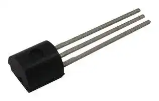
- Transistor Case Style: TO-92
- Drain Source Voltage Vds: 60V
- Operating Temperature Max: 150°C
- Continuous Drain Current Id: 640mA
- Drain Source On State Resistance: 0.75ohm
- Gate Source Threshold Voltage Max: 3.5V
| Delivery and price | |
|---|---|
| Units per pack | 1000 |
| Price | 1.43 € |
| Current stock | 100+ |
| Lead time | 30 days |
_**Su ertex inc. p**_

**VP2206**

## **P-Channel Enhancement-Mode Vertical DMOS FET**

## **Features**

- Free from secondary breakdown

- Low power drive requirement

- Ease of paralleling

- Low CISS and fast switching speeds

- High input impedance and high gain

- Excellent thermal stability

- Integral source-to-drain diode

## **Applications**

## **General Description**

The Supertex VP2206 is an enhancement-mode (normallyoff) transistor that utilizes a vertical DMOS structure and Supertex’s well-proven silicon-gate manufacturing process. This combination produces a device with the power handling capabilities of bipolar transistors, and the high input impedance and positive temperature coefficient inherent in MOS devices. Characteristic of all MOS structures, this device is free from thermal runaway and thermally-induced secondary breakdown.

- Motor controls

- Converters, amplifiers, and switches

- Power supply circuits

- Drivers (relays, hammers, solenoids, lamps,

- memories, displays, bipolar transistors, etc.)

Supertex’s vertical DMOS FETs are ideally suited to a wide range of switching and amplifying applications where very low threshold voltage, high breakdown voltage, high input impedance, low input capacitance, and fast switching speeds are desired.

**Ordering Information Product Summary Package Part Number Option Packing BVDSS/BVDGS R(max)DS(ON) I(min)D(ON)** VP2206N2-G TO-39 500/Bag VP2206N3-G TO-92 1000/Bag -60V 0.9Ω -4.0A VP2206N3-G P002VP2206N3-G P003 **Pin Configuration** VP2206N3-G P005 TO-92 2000/Reel VP2206N3-G P013 ~ @ ~~=Tle«~~ VP2206N3-G P014 **GATE DRAIN** _-G denotes a lead (Pb)-free / RoHS compliant package._ **SOURCE SOURCE** _Contact factory for Wafer / Die availablity. Devices in Wafer / Die form are lead (Pb)-free / RoHS compliant._ **DRAIN GATE Absolute Maximum Ratings TO-39 TO-92 Parameter Value Product Marking** Drain-to-source voltage BVDSS Drain-to-gate voltage BVDGS **2206N2       VP** YY = Year Sealed Gate-to-source voltage ±20V **YYWW** WW = Week Sealed Operating and storage temperature -55[O] C to +150[O] C _Package may or may not include the following marks: Si or Absolute Maximum Ratings are those values beyond which damage to the device may occur. Functional operation under these conditions is not implied. Continuous_ **TO-39** ~~——~~ | _operation of the device at the absolute rating level may affect device reliability. All voltages are referenced to device ground._ **SiVP** YY = Year Sealed **Typical Thermal Resistance Y Y W W  2 2 0 6** WW = Week Sealed = “Green” Packaging **Package** _**θja** Package may or may not include the following marks: Si or_ TO-39 N/A **TO-92** TO-92 132[O] C/W ~~— io~~ _Doc.# DSFP-VP2206_ _**Supertex inc.** E082313_

_**Supertex inc. www.supertex.com**_

**VP2206**

## **Thermal Characteristics**

|**Package**|**ID**<br>**(continuous)****_†_**|**ID**<br>**(pulsed)**|**Power Dissipation**<br>**@TC = 25OC**|**IDR**<br>**_†_**|**IDRM**|
|---|---|---|---|---|---|
|TO-39|-750mA|-8.0A|0.36W|-750mA|-8.0A|
|TO-92|-640mA|-4.0|0.74W|-640mA|-4.0|


_**Notes:**_

_†    ID (continuous) is limited by max rated Tj ._

## **Electrical Characteristics** _(TA = 25[O] C unless otherwise specified)_

**==> picture [542 x 376] intentionally omitted <==**

**----- Start of picture text -----**<br>
Sym Parameter Min Typ Max Units Conditions<br>BVDSS Drain-to-source breakdown voltage -60 - - V VGS = 0V, ID = -10mA<br>VGS(th) Gate threshold voltage -1.0 - -3.5 V VGS = VDS, ID= -10mA<br>ΔVGS(th) Change in VGS(th) with temperature - -4.3 -5.5 mV/ [O] C VGS = VDS, ID= -10mA<br>IGSS Gate body leakage - -1.0 -100 nA VGS = ± 20V, VDS = 0V<br>- - -50 µA VGS = 0V, VDS = Max Rating<br>IDSS Zero gate voltage drain current - - -10 mA VDS = 0.8 Max Rating,<br>VGS = 0V, TA = 125°C<br>I On-state drain current -0.85 -2.0 - VGS = -5.0V, VDS = -25V<br>D(ON) -4.0 -9.0 - A VGS = -10V, VDS = -25V<br>R Static drain-to-source on-state resistance - 1.3 1.5 Ω VGS = -5.0V, ID = -1.0A<br>DS(ON) - 0.75 0.9 VGS = -10V, ID = -3.5A<br>ΔRDS(ON) Change in RDS(ON) with temperature - 0.85 1.2 %/ [O] C VGS = -10V, ID = -3.5A<br>GFS Forward transductance 800 1400 - mmho  VDS = -25V, ID = -2.0A<br>CISS Input capacitance - 325 450 VGS = 0V,<br>COSS Common source output capacitance - 125 180 pF VDS = -25V,<br>CRSS Reverse transfer capacitance - 30 40 f = 1.0MHz<br>td(ON) Turn-on delay time  - 4.0 15<br>t Rise time - 16 25 VDD = -25V,<br>r ns ID = -4.0A,<br>td(OFF) Turn-off delay time - 16 50 R  = 10Ω<br>GEN<br>t Fall time - 22 50<br>f<br>VSD Diode forward voltage drop - -1.1 -1.6 V VGS = 0V, ISD = -3.5A<br>trr Reverse recovery time - 500 - ns VGS = 0V, ISD = -1.0A<br>**----- End of picture text -----**<br>


_**Notes:**_

_1. All D.C. parameters 100% tested at 25[O] C unless otherwise stated. (Pulse test: 300µs pulse, 2% duty cycle.)_

_2. All A.C. parameters sample tested._

## **Switching Waveforms and Test Circuit**

**==> picture [420 x 114] intentionally omitted <==**

**----- Start of picture text -----**<br>
0V Pulse<br>10%<br>Generator<br>INPUT<br>-10V 90% RGEN<br>t(ON) t(OFF)<br>D.U.T.<br>td(ON) tr td(OFF) tf INPUT<br>OUTPUT<br>0V<br>OUTPUT 90% 90% RL<br>10% 10%<br>VDD<br>VDD<br>**----- End of picture text -----**<br>


_**Supertex inc.**_

_Doc.# DSFP-VP2206 E082313_

_**www.supertex.com**_

2

**VP2206**

## **Typical Performance Curves**

## **BVDSS Variation with Temperature**

**==> picture [191 x 183] intentionally omitted <==**

**----- Start of picture text -----**<br>
1.1<br>1.0<br>0.9<br>-50                   0                     50                   100                  150<br>Tj ( [O] C)<br>(normalized)<br>DSS<br>BV<br>**----- End of picture text -----**<br>


**==> picture [191 x 410] intentionally omitted <==**

**----- Start of picture text -----**<br>
Transfer Characteristics<br>-10<br>VDS = -25V<br>-8.0<br>-6.0<br>-4.0<br>-2.0<br>0<br>0              -2.0             -4.0             -6.0             -8.0              -10<br>VGS (volts)<br>Capacitance vs. Drain-to-Source Voltage<br>400<br>f = 1.0MHz<br>CISS<br>300<br>200<br>100<br>0<br>0                   -10                   -20                   -30                  -40<br>VDS (volts)<br>TA = -55OC<br>COSS<br>CRSS<br>25OC<br>125OC<br>(amperes)<br>ID<br>C (picofarads)<br>**----- End of picture text -----**<br>


## **Capacitance vs. Drain-to-Source Voltage**

## **On-Resistance vs. Drain Current**

**==> picture [216 x 404] intentionally omitted <==**

**----- Start of picture text -----**<br>
5.0<br>VGS = -5.0V<br>4.0<br>3.0<br>2.0<br>VGS = -10V<br>1.0<br>0<br>0              -2.0             -4.0             -6.0             -8.0              -10<br>ID (amperes)<br> V(th) and RDS Variation with Temperature<br>1.2  2.0<br>RDS(ON) @ -10V, -3.5A<br>1.1  1.6<br>1.0  1.2<br>0.9  0.8<br>V(th) @ -1.0mA<br>0.8  0.4<br>0.7  0<br>-50                   0                     50                   100                  150<br>Tj ( [O] C)<br>(ohms)<br>DS(ON)<br>R<br>(normalized) (normalized)<br>GS(th)  DS(ON)<br>V R<br>**----- End of picture text -----**<br>


**Gate Drive Dynamic Characteristics**

**==> picture [191 x 183] intentionally omitted <==**

**----- Start of picture text -----**<br>
-10<br>-8.0<br>VDS = -10V  VDS = -40V<br>-6.0<br>725 pF<br>-4.0<br>-2.0<br>310 pF<br>0 0               2.0               4.0              6.0              8.0               10<br>QG (nanocoulombs)<br>(volts)<br>GS<br>V<br>**----- End of picture text -----**<br>


_**Supertex inc.**_

_Doc.# DSFP-VP2206 E082313_

_**www.supertex.com**_

3

**VP2206**

## **Typical Performance Curves** _**(cont.)**_

## **Output Characteristics**

**==> picture [199 x 194] intentionally omitted <==**

**----- Start of picture text -----**<br>
-10<br>VGS = -10V<br>-8.0<br>-6.0  -8V<br>-4.0<br>-6V<br>-2.0<br>-4V<br>-3V<br>0<br>0                -10               -20               -30               -40              -50<br>VDS (volts)<br>(amperes)<br>ID<br>**----- End of picture text -----**<br>


## **Transconductance vs. Drain Current**

**==> picture [199 x 194] intentionally omitted <==**

**----- Start of picture text -----**<br>
2.0<br>VDS = -25V<br>TA = -55 [O] C<br>TA = 25 [O] C  TA = 125 [O] C<br>1.0<br>0<br>0                                              -5.0                                             -10<br>ID (amperes)<br>(siemens)<br>FS<br>G<br>**----- End of picture text -----**<br>


## **Maximum Rated Safe Operating Area**

**==> picture [200 x 193] intentionally omitted <==**

**----- Start of picture text -----**<br>
-10<br>TO-39 (pulsed)<br>TO-92 (pulsed)<br>TO-39 (DC)<br>-1.0<br>TO-92 (DC)<br>-0.1<br>TC = 25 [O] C<br>-0.01<br>-1.0                          -10                            -100                       -1000<br>VDS (volts)<br>(amperes)<br>ID<br>**----- End of picture text -----**<br>


## **Saturation Characteristics**

**==> picture [203 x 647] intentionally omitted <==**

**----- Start of picture text -----**<br>
-10<br>VGS = -10V<br>-8.0<br>-8V<br>-6.0<br>-4.0<br>-6V<br>-2.0<br>-4V<br>-3V<br>0<br>0                -2.0              -4.0              -6.0              -8.0              -10<br>VDS (volts)<br>Power Dissipation vs. Case Temperature<br>10<br>8.0<br>TO-39<br>6.0<br>4.0<br>2.0<br>TO-92<br>0<br>0             25            50             75            100           125           150<br>TC ( [O] C)<br>Thermal Response Characteristics<br>10<br>8.0<br>6.0<br>TO-39<br>PD = 6.0W<br>TC = 25 [O] C<br>4.0<br>TO-92<br>2.0  PD = 1.0W<br>TC = 25 [O] C<br>0<br>0.001              0.01                   0.1                    1.0                     10<br>tP (seconds)<br>(amperes)<br>ID<br>(watts)<br>D<br>P<br>Thermal Resistance (normalized)<br>**----- End of picture text -----**<br>


**==> picture [195 x 10] intentionally omitted <==**

**----- Start of picture text -----**<br>
Power Dissipation vs. Case Temperature<br>**----- End of picture text -----**<br>


_**Supertex inc.**_

_Doc.# DSFP-VP2206 E082313_

_**www.supertex.com**_

4

**VP2206**

## **3-Lead TO-39 Package Outline (N2)**

**==> picture [177 x 201] intentionally omitted <==**

**----- Start of picture text -----**<br>
Φa<br>β β<br>2<br>1 3<br>α<br>k<br>j<br>**----- End of picture text -----**<br>


**Bottom View**

**==> picture [212 x 264] intentionally omitted <==**

**----- Start of picture text -----**<br>
ΦD<br>ΦD1<br>A<br>Seating<br>h Plane<br>1 2 3<br>Φb<br>L<br>**----- End of picture text -----**<br>


**Side View**

**==> picture [542 x 73] intentionally omitted <==**

**----- Start of picture text -----**<br>
Symbol α β A Φ a Φ b Φ D Φ D1 h j k L<br>MIN .240 .190 .016 .350 .315 .009 .028 .029 .500<br>Dimension 45 [O] 90 [O]<br>NOM - - - - - - - - -<br>(inches) NOM NOM<br>MAX .260 .210 .021 .370 .335 .125 .034 .040 .560*<br>**----- End of picture text -----**<br>


_JEDEC Registration TO-39. * This dimension is not specified in the JEDEC drawing._ _**Drawings not to scale.**_

_**Supertex Doc. #:** DSPD-3TO39N2, Version B052009._

_**Supertex inc. www.supertex.com**_

_Doc.# DSFP-VP2206 E082313_

5

**VP2206**

## **3-Lead TO-92 Package Outline (N3)**

**==> picture [295 x 241] intentionally omitted <==**

**----- Start of picture text -----**<br>
D<br>A<br>Seating<br>Plane 1     2     3<br>L<br>b c<br>e1<br>e<br>Front View  Side View<br>**----- End of picture text -----**<br>


**==> picture [131 x 67] intentionally omitted <==**

**----- Start of picture text -----**<br>
E<br>E1<br>1 3<br>2<br>**----- End of picture text -----**<br>


**==> picture [80 x 10] intentionally omitted <==**

**----- Start of picture text -----**<br>
Bottom View<br>**----- End of picture text -----**<br>


**==> picture [542 x 74] intentionally omitted <==**

**----- Start of picture text -----**<br>
Symbol A b c D E E1 e e1 L<br>MIN .170 .014 [†] .014 [†] .175 .125 .080 .095 .045 .500<br>Dimensions<br>NOM - - - - - - - - -<br>(inches)<br>MAX .210 .022 [†] .022 [†] .205 .165 .105 .105 .055 .610*<br>**----- End of picture text -----**<br>


_JEDEC Registration TO-92._

- _This dimension is not specified in the JEDEC drawing._

_† This dimension differs from the JEDEC drawing._

_**Drawings not to scale.**_

_**Supertex Doc.#:** DSPD-3TO92N3, Version E041009._

_(The package drawing(s) in this data sheet may not reflect the most current specifications. For the latest package outline information go to http://www.supertex.com/packaging.html.)_

_**Supertex inc.**_ does not recommend the use of its products in life support applications, and will not knowingly sell them for use in such applications unless it receives an adequate “product liability indemnification insurance agreement.” _**Supertex inc.**_ does not assume responsibility for use of devices described, and limits its liability to the replacement of the devices determined defective due to workmanship. No responsibility is assumed for possible omissions and inaccuracies. Circuitry and specifications are subject to change without notice. For the latest product specifications refer to the _**Supertex inc.**_ (website: http//www.supertex.com)

> ©2013 _**Supertex inc.**_ All rights reserved. Unauthorized use or reproduction is prohibited.

_**Supertex inc.**_ 1235 Bordeaux Drive, Sunnyvale, CA 94089 Tel: 408-222-8888 _**www.supertex.com**_

_Doc.# DSFP-VP2206 E082313_

6
Updated at April 29, 2026
Microchip Technology Inc. is a leading global provider of smart, connected, and secure embedded control solutions. Known for enabling engineers to design with confidence, the company delivers a comprehensive product portfolio that reduces total system costs and accelerates time to market across the industrial, automotive, communications, and computing sectors. Our extensive selection of Microchip components highlights the manufacturer's strength in both discrete semiconductors and advanced wireless connectivity. We carry a robust lineup of highly efficient single MOSFETs and Schottky diodes tailored for demanding power management and switching applications. Alongside these essential discretes, engineers can source a wide array of ready-to-use networking modules, prominently featuring Bluetooth and WLAN adapters that streamline the development of modern IoT and connected devices. Rounding out the offering is a diverse range of Microchip integrated circuits and specialized components. This includes versatile I/O expanders for simplified system integration, precision timing solutions such as MEMS oscillators and pulse generators, as well as AC/DC LED driver ICs and sub-2.4GHz RF transceivers. Backed by Microchip's renowned commitment to exceptional quality and reliable performance, these components provide scalable, dependable building blocks for complex electronic designs.
About Novapart
Novapart is a B2B electronic component broker specialising in stock shortages and cost reduction. We source hard-to-find parts and identify compliant alternatives across a catalogue of 410,000+ components from 500+ manufacturers.
Learn more →Stock Shortage Specialist
When a component is unavailable, discontinued or has an unacceptable lead time, we tap into our network of vetted European and Asian distributors to source what you need — without compromising on quality or traceability.
Request a quote →Compliant Alternatives
We identify pin-to-pin, electrically equivalent substitutes that meet the same certifications (RoHS, AEC-Q100, REACH) as your original specification — validated against datasheets, not just part numbers. Often at a lower cost.
BOM Analysis service →