


VO14642AABTR
MOSFET Relay, SPST-NO (1 Form A), AC / DC, 60 V, 2 A, SMD-6, Surface Mount
- Manufacturer: VISHAY
- Product type: MOSFET Solid State Relays
- Contact Configuration:SPST-NO; Load Current:2A; Relay Terminals:Solder; Load Voltage Max:60V; On State Resistance Max:0.25ohm; Isolation Voltage:5.3kV; Forward Current If:50mA; Produc
- SVHC: No SVHC (07-Nov-2024)
- Load Type: AC / DC
- Contact Form: SPST-NO (1 Form A)
- Load Current: 2A
- Product Range: VO14642 Series
- Relay Mounting: Surface Mount
- Relay Terminals: Gull Wing
- Load Voltage Max: 60V
- Isolation Voltage: 5.3kV
- I/O Capacitance Typ: -
- On State Resistance Max: 0.25ohm
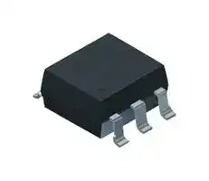
- MOSFET Relay Package Style: SMD-6
- Off State Leakage Current Max: 1µA
| Delivery and price | |
|---|---|
| Units per pack | 100 |
| Price | 1.6 € |
| Current stock | 10+ |
| Lead time | 30 days |
**VO14642AT, VO14642AABTR**

## VISHAY. ~~—~~

www.vishay.com

Vishay Semiconductors

## **1 Form A Solid-State Relay**

## **FEATURES**

**==> picture [174 x 91] intentionally omitted <==**

**----- Start of picture text -----**<br>
S DC S'<br>6 5 4<br>oe ie<br>**----- End of picture text -----**<br>


**==> picture [63 x 94] intentionally omitted <==**

**----- Start of picture text -----**<br>
S DC S'<br>6 5 4<br>ie<br>1 2 3<br>**----- End of picture text -----**<br>


- High speed SSR - ton/toff < 800 μs

- Maximum RON 0.25 Ω

- Isolation test voltage 5300 VRMS

- Load voltage 60 V

- Load current 2 ADC configuration

- DIP-6 package

- Clean bounce free switching

- TTL / CMOS compatible input

- Available on tape and reel

- Material categorization: for definitions of compliance please see www.vishay.com/doc?99912 ~~So~~

## **APPLICATIONS**

## **LINKS TO ADDITIONAL RESOURCES**

- Instrumentation

- Industrial controls

- Security

Product Page Design Tools Models

- Automatic measurement equipment

## **DESCRIPTION**

The VO14642 is a high speed single channel normally open solid-state relay (SPST - 1 form A) in a DIP-6 package. The relay is constructed as a multi-chip hybrid device. A high efficient infrared LED enables low forward current on the input side. On the output side high performance MOSFET switches provide a low RON and can be configured for

AC/DC or DC only operation.

## **AGENCY APPROVALS**

- UL 1577

- cUL

- DIN EN 60747-5-5 (VDE 0884-5)

- FIMKO

## **Note**

• Agency approvals are valid only for ambient temperature range -40 °C to +85 °C

**ORDERING INFORMATION** ~~pT~~ DIP-6 SMD-6 **V O 1 4 6 4 2 A x x T R** PART NUMBER ELECTR. PACKAGE TAPE AND ~~JOOCUOGGO0C0~~ VARIATION CONFIG. REEL ~~mm -,~~ **PACKAGE** ~~a~~ SMD-6, tape and reel VO14642AABTR ~~pC~~ DIP-6, Tubes VO14642AT ~~pf~~

Rev. 1.8, 21-Aug-2023

Document Number: 81646

**1**

For technical questions, contact: optocoupleranswers@vishay.com THIS DOCUMENT IS SUBJECT TO CHANGE WITHOUT NOTICE. THE PRODUCTS DESCRIBED HEREIN AND THIS DOCUMENT ARE SUBJECT TO SPECIFIC DISCLAIMERS, SET FORTH AT www.vishay.com/doc?91000

**VO14642AT, VO14642AABTR**

www.vishay.com

## Vishay Semiconductors

|**ABSOLUTE MAXIMUM RATINGS**(Tamb= 25 °C,unless otherwise specified)|**ABSOLUTE MAXIMUM RATINGS**(Tamb= 25 °C,unless otherwise specified)|**ABSOLUTE MAXIMUM RATINGS**(Tamb= 25 °C,unless otherwise specified)|**ABSOLUTE MAXIMUM RATINGS**(Tamb= 25 °C,unless otherwise specified)|**ABSOLUTE MAXIMUM RATINGS**(Tamb= 25 °C,unless otherwise specified)|
|---|---|---|---|---|
|**PARAMETER**|**TEST CONDITION**|**SYMBOL**|**VALUE**|**UNIT**|
|**INPUT**|||||
|LED continous forward current||IF|50|mA|
|LED reverse voltage||VR|5|V|
|LEDpower dissipation|At 25 °C|Pdiss|80|mW|
|**OUTPUT**|||||
|DC orpeak AC load voltage||VL|60|V|
|Load current(DC only)||IL|2000|mA|
|Peak load current(AC/DC)|t = 10 ms|ILPK|3.6|A|
|Outputpower dissipation|At 25 °C|Pdiss|250|mW|
|**SSR**|||||
|Totalpower dissipation||Pdiss|330|mW|
|Ambient temperature range||Tamb|-55 to +85|°C|
|Storage temperature range||Tstg|-55 to +125|°C|
|Solderingtemperature(1)|t≤10 s max.|Tsld|260|°C|


## **Notes**

- Stresses in excess of the absolute maximum ratings can cause permanent damage to the device. Functional operation of the device is not implied at these or any other conditions in excess of those given in the operational sections of this document. Exposure to absolute maximum ratings for extended periods of the time can adversely affect reliability.

- (1) Refer to reflow profile for soldering conditions for surface mounted devices (SMD). Refer to wave profile for soldering conditions for through hole devices (DIP).

## **ABSOLUTE MAXIMUM RATING CURVE**

**==> picture [174 x 149] intentionally omitted <==**

**----- Start of picture text -----**<br>
2.5<br>DC mode<br>2.0<br>1.5<br>AC/DC mode<br>1.0<br>0.5<br>0.0<br>-50 -25 0 25 50 75 100<br>Ambient Temperature/°C<br>Load Current/A<br>**----- End of picture text -----**<br>


Fig. 1 - Load Current (AC/DC) vs. Temperature

|**THERMAL CHARACTERISTICS**|**THERMAL CHARACTERISTICS**|**THERMAL CHARACTERISTICS**|**THERMAL CHARACTERISTICS**|**THERMAL CHARACTERISTICS**|
|---|---|---|---|---|
|**PARAMETER**|**TEST CONDITION**|**SYMBOL**|**VALUE**|**UNIT**|
|Maximum LED junction temperature|At 25 °C|Tjmax.|125|°C|
|Maximum output die junction temperature|At 25 °C|Tjmax.|125|°C|
|Thermal resistance,junction emitter to board|At 25 °C|θEB|176|°C/W|
|Thermal resistance,junction emitter to case|At 25 °C|θEC|208|°C/W|
|Thermal resistance,junction detector to board|At 25 °C|θDB|67|°C/W|
|Thermal resistance,junction detector to case|At 25 °C|θDC|134|°C/W|
|Thermal resistance,junction emitter tojunction detector|At 25 °C|θED|310|°C/W|
|Thermal resistance, case to ambient|At 25 °C|θCA|2180|°C/W|


## **Note**

- The thermal model is represented in the thermal network below. Each resistance value given in this model can be used to calculate the temperatures at each node for a given operating condition. The thermal resistance from board to ambient will be dependent on the type of PCB, layout and thickness of copper traces. For a detailed explanation of the thermal model, please reference Vishay's thermal characteristics of optocouplers application note.

Rev. 1.8, 21-Aug-2023

Document Number: 81646

**2** For technical questions, contact: optocoupleranswers@vishay.com THIS DOCUMENT IS SUBJECT TO CHANGE WITHOUT NOTICE. THE PRODUCTS DESCRIBED HEREIN AND THIS DOCUMENT ARE SUBJECT TO SPECIFIC DISCLAIMERS, SET FORTH AT www.vishay.com/doc?91000

**VO14642AT, VO14642AABTR**

www.vishay.com

## Vishay Semiconductors

**==> picture [138 x 181] intentionally omitted <==**

**----- Start of picture text -----**<br>
TA<br>θCA<br>Package<br>TC<br>θDC θEC<br>TJD θDE TJE<br>θDB<br>θEB<br>TB<br>θBA<br>19996<br>TA<br>**----- End of picture text -----**<br>


|**ELECTRICAL CHARACTERISTICS**(Tamb= 25 °C,unless otherwise specified)|**ELECTRICAL CHARACTERISTICS**(Tamb= 25 °C,unless otherwise specified)|**ELECTRICAL CHARACTERISTICS**(Tamb= 25 °C,unless otherwise specified)|**ELECTRICAL CHARACTERISTICS**(Tamb= 25 °C,unless otherwise specified)|**ELECTRICAL CHARACTERISTICS**(Tamb= 25 °C,unless otherwise specified)|**ELECTRICAL CHARACTERISTICS**(Tamb= 25 °C,unless otherwise specified)|**ELECTRICAL CHARACTERISTICS**(Tamb= 25 °C,unless otherwise specified)|
|---|---|---|---|---|---|---|
|**PARAMETER**|**TEST CONDITION**|**SYMBOL**|**MIN.**|**TYP.**|**MAX.**|**UNIT**|
|**INPUT**|||||||
|LED forward current, switch turn-on|IL= 1 A, VL ≤0.5 V, t = 10 ms|IFon|-|0.5|2|mA|
|LED forward current, switch turn-off|VL= 60 V, IL< 1 μA|IFoff|50|-|-|μA|
|LED reverse current|VR= 5 V|IR|-|-|10|μA|
|LED forward voltage|IF= 10 mA|VF|1.0|1.4|1.6|V|
|**OUTPUT**|||||||
|On-resistance (AC/DC)|IF= 10 mA, IL= 1 A|RON|-|0.18|0.25|Ω|
|On-resistance (DC only)|IF= 10 mA, IL= 2 A|RON|-|0.05|0.07|Ω|
|Off-state leakage current|IF= 0 mA, VL= 60 V|ILEAK|-|-|1|μA|


## **Note**

- Minimum and maximum values are testing requirements. Typical values are characteristics of the device and are the result of engineering evaluations. Typical values are for information only and are not part of the testing requirements.

## **PIN CONFIGURATION**

**==> picture [287 x 90] intentionally omitted <==**

**----- Start of picture text -----**<br>
AC/DC configuration DC only configuration<br>1 6 1 6<br>Anode Load Anode<br>2 5 2 5<br>Cathode Cathode<br>3 4 3 4<br>Do not use Load Do not use<br>20545<br>**----- End of picture text -----**<br>


|**SWITCHING CHARACTERISTICS(AC/DC CONNECTION)**|**SWITCHING CHARACTERISTICS(AC/DC CONNECTION)**|**SWITCHING CHARACTERISTICS(AC/DC CONNECTION)**|**SWITCHING CHARACTERISTICS(AC/DC CONNECTION)**|**SWITCHING CHARACTERISTICS(AC/DC CONNECTION)**|**SWITCHING CHARACTERISTICS(AC/DC CONNECTION)**|**SWITCHING CHARACTERISTICS(AC/DC CONNECTION)**|
|---|---|---|---|---|---|---|
|**PARAMETER**|**TEST CONDITION**|**SYMBOL**|**MIN.**|**TYP.**|**MAX.**|**UNIT**|
|Turn-on time|IF= 10 mA, VL= 30 V, IL= 200 mA|ton|-|370|800|μs|
|Turn-off time|IF= 10 mA, VL= 30 V, IL= 200 mA|toff|-|50|800|μs|
|Turn-on time|IF= 10 mA, VL= 5 V, IL= 1 A|ton|-|550|-|μs|
|Turn-off time|IF= 10 mA, VL= 5 V, IL= 1 A|toff|-|18|-|μs|


Rev. 1.8, 21-Aug-2023

Document Number: 81646

**3**

For technical questions, contact: optocoupleranswers@vishay.com THIS DOCUMENT IS SUBJECT TO CHANGE WITHOUT NOTICE. THE PRODUCTS DESCRIBED HEREIN AND THIS DOCUMENT ARE SUBJECT TO SPECIFIC DISCLAIMERS, SET FORTH AT www.vishay.com/doc?91000

**VO14642AT, VO14642AABTR**

**==> picture [77 x 10] intentionally omitted <==**

**----- Start of picture text -----**<br>
www.vishay.com<br>**----- End of picture text -----**<br>


## Vishay Semiconductors

**==> picture [398 x 171] intentionally omitted <==**

**----- Start of picture text -----**<br>
VL<br>1.25 ms<br>Input<br>Output<br>T<br>ON<br>T<br>OFF<br>Output 90 %<br>10 %<br>20991-1<br>**----- End of picture text -----**<br>


|**SAFETY AND INSULATION RATINGS**|**SAFETY AND INSULATION RATINGS**|**SAFETY AND INSULATION RATINGS**|**SAFETY AND INSULATION RATINGS**|**SAFETY AND INSULATION RATINGS**|
|---|---|---|---|---|
|**PARAMETER**|**TEST CONDITION**|**SYMBOL**|**VALUE**|**UNIT**|
|Climatic classification|Accordingto IEC 68 part 1||40 / 085 / 21||
|Pollution degree|According to DIN VDE 0109||2||
|Comparative trackingindex|Insulationgroup IIIa|CTI|175||
|Maximum rated withstandingisolation voltage|Accordingto UL1577, t = 1 min|VISO|5300|VRMS|
|Maximum transient isolation voltage|According to DIN EN 60747-5-5|VIOTM|8000|Vpeak|
|Maximum repetitive peak isolation voltage|Accordingto DIN EN 60747-5-5|VIORM|890|Vpeak|
|Isolation resistance|Tamb= 25 °C, VIO= 500 V|RIO|≥1012|Ω|
||Tamb= 100 °C, VIO= 500 V|RIO|≥1011|Ω|
||Tamb= TS, VIO= 500 V|RIO|≥109|Ω|
|Output safety power||PSO|400|mW|
|Input safety current||ISI|150|mA|
|Input safety temperature||TS|165|°C|
|Creepage distance|||≥7|mm|
|Clearance distance|||≥7|mm|
|Insulation thickness||DTI|≥0.4|mm|


## **Note**

- This SSR is suitable for “safe electrical insulation” only within the safety ratings. Compliance with the safety ratings shall be ensured by means of protective circuits.

**==> picture [176 x 154] intentionally omitted <==**

**----- Start of picture text -----**<br>
450<br>400<br>350 Output Power P SO<br>300<br>250<br>200<br>150<br>100<br>50<br>0<br>0 25 50 75 100 125 150 175 200<br>Ambient Temperature (°C)<br>Maximum Safety Output Power (mW)<br>**----- End of picture text -----**<br>


Fig. 2 - Safety Derating (output)

Rev. 1.8, 21-Aug-2023

**==> picture [177 x 154] intentionally omitted <==**

**----- Start of picture text -----**<br>
160<br>140<br>120<br>100<br>80<br>60 Input Current I SI<br>40<br>20<br>0<br>0 25 50 75 100 125 150 175 200<br>Ambient Temperature (°C)<br>Maximum Safety Input Current (mA)<br>**----- End of picture text -----**<br>


Fig. 3 - Safety Derating (input)

Document Number: 81646

**4**

For technical questions, contact: optocoupleranswers@vishay.com THIS DOCUMENT IS SUBJECT TO CHANGE WITHOUT NOTICE. THE PRODUCTS DESCRIBED HEREIN AND THIS DOCUMENT ARE SUBJECT TO SPECIFIC DISCLAIMERS, SET FORTH AT www.vishay.com/doc?91000

**VO14642AT, VO14642AABTR**

**==> picture [77 x 10] intentionally omitted <==**

**----- Start of picture text -----**<br>
www.vishay.com<br>**----- End of picture text -----**<br>


## Vishay Semiconductors

## **TYPICAL CHARACTERISTICS** (Tamb = 25 °C, unless otherwise specified)

**==> picture [209 x 593] intentionally omitted <==**

**----- Start of picture text -----**<br>
100 10000<br>10 Tamb = 85 °C 1000<br>Tamb = 25 °C<br>1 100<br>Tamb = -55 °C<br>0.1 10<br>0.8 1.0 1.2 1.4 1.6 1.8<br>VF - Forward Voltage (V)<br>Fig. 4 - Forward Voltage vs. Forward Current<br>Axis Title<br>1.0 10000<br>0.9 V R  = 5 V<br>0.8<br>0.7<br>1000<br>0.6<br>0.5<br>0.4<br>100<br>0.3<br>0.2<br>0.1<br>0 10<br>-55 -35 -15 5 25 45 65 85<br>Ambient Temperature (°C)<br>Fig. 5 - LED Leakage Current vs. Ambient Temperature<br>Axis Title<br>20 10000<br>VLOAD = 60 V<br>15<br>1000<br>10<br>100<br>5<br>0 10<br>-55 -35 -15 5 25 45 65 85<br>Ambient Temperature (°C)<br>Fig. 6 - Leakage Current vs. Temperature<br> - Forward Current (mA)IF<br>Leakage Current (nA)<br>Leakage Current (nA)<br>**----- End of picture text -----**<br>


**==> picture [217 x 601] intentionally omitted <==**

**----- Start of picture text -----**<br>
Axis Title<br>1.7 10000<br>1.6 IF = 50 mA<br>IF = 30 mA<br>1.5<br>1000<br>1.4<br>1.3<br>IF = 10 mA<br>100<br>1.2<br>IF = 5 mA<br>1.1 IF = 1 mA<br>1.0 10<br>-55 -35 -15 5 25 45 65 85<br>Ambient Temperature (°C)<br>Fig. 7 - LED Voltage vs. Temperature<br>Axis Title<br>1.6 10000<br>IL = 100 mA<br>1.4<br>1000<br>1.2<br>100<br>1.0<br>Normalized to Tamb = 25°C<br>0.8 10<br>-40 -20 0 20 40 60 80<br>Ambient Temperature (°C)<br>Fig. 8 - LED Forward Current for Switch Turn-On vs.<br>Ambient Temperature<br>Axis Title<br>1.8 10000<br>IF = 10 mA,<br>1.6 I L  = 1 A<br>1.4<br>1000<br>1.2<br>1.0<br>100<br>0.8<br>0.6<br>0.4 10<br>-55 -35 -15 5 25 45 65 85<br>Temperature (°C)<br>Fig. 9 - On-Resistance vs. Temperature<br>2nd line<br> - Forward Voltage (V)VF<br>2<br>for Switch Turn-On<br>Normalized Forward Current<br>Line 1<br>On-Resistance, Normalized to 25 °C<br>**----- End of picture text -----**<br>


Rev. 1.8, 21-Aug-2023

Document Number: 81646

**5**

For technical questions, contact: optocoupleranswers@vishay.com THIS DOCUMENT IS SUBJECT TO CHANGE WITHOUT NOTICE. THE PRODUCTS DESCRIBED HEREIN AND THIS DOCUMENT ARE SUBJECT TO SPECIFIC DISCLAIMERS, SET FORTH AT www.vishay.com/doc?91000

**VO14642AT, VO14642AABTR**

## www.vishay.com

**==> picture [209 x 170] intentionally omitted <==**

**----- Start of picture text -----**<br>
Axis Title<br>85 10000<br>82 I F  = 10 mA, I L  = 1 A, t P  = 5 ms<br>79<br>76<br>1000<br>73<br>70<br>67<br>100<br>64<br>61<br>58<br>55 10<br>-55 -35 -15 5 25 45 65 85<br>Ambient Temperature (°C)<br>Turn-Off Time (μs)<br>**----- End of picture text -----**<br>


Fig. 10 - Turn-Off Time vs. Temperature

**==> picture [209 x 170] intentionally omitted <==**

**----- Start of picture text -----**<br>
Axis Title<br>100 10000<br>IL = 1 A, tP = 5 ms, Tamb = 25 °C<br>80<br>1000<br>60<br>100<br>40<br>20 10<br>5 10 15 20<br>Forward Current (mA)<br> - Turn-Off Time (µs)<br>toff<br>**----- End of picture text -----**<br>


**==> picture [156 x 8] intentionally omitted <==**

**----- Start of picture text -----**<br>
Fig. 11 - Turn-Off Time vs. Forward Current<br>**----- End of picture text -----**<br>


## Vishay Semiconductors

**==> picture [209 x 170] intentionally omitted <==**

**----- Start of picture text -----**<br>
Axis Title<br>1020 10000<br>IL = 1 A, tP = 5 ms, Tamb = 25°C<br>920<br>820<br>1000<br>720<br>620<br>520<br>100<br>420<br>320<br>220 10<br>5 10 15 20<br>Forward Current (mA)<br> - Turn-On Time (µs)<br>ton<br>**----- End of picture text -----**<br>


Fig. 13 - Turn-On Time vs. Forward Current

**==> picture [209 x 184] intentionally omitted <==**

**----- Start of picture text -----**<br>
Axis Title<br>250 10000<br>Tamb = -55 °C<br>200<br>1000<br>150<br>100<br>100<br>50<br>0 10<br>0 10 20 30 40 50 60<br>Applied Voltage (V)<br>Fig. 14 - Switch Capacitance vs. Applied Voltage<br>Switch Caoacitance (pF)<br>**----- End of picture text -----**<br>


**==> picture [209 x 184] intentionally omitted <==**

**----- Start of picture text -----**<br>
Axis Title<br>700 10000<br>IF = 10 mA, IL = 1 A, tP = 5 ms<br>650<br>600 1000<br>550<br>500 100<br>450<br>400 10<br>-55 -35 -15 5 25 45 65 85<br>Ambient Temperature (°C)<br>Fig. 12 - Turn-On Time vs. Temperature<br>Turn-On Time (μs)<br>**----- End of picture text -----**<br>


Rev. 1.8, 21-Aug-2023

Document Number: 81646

**6**

For technical questions, contact: optocoupleranswers@vishay.com THIS DOCUMENT IS SUBJECT TO CHANGE WITHOUT NOTICE. THE PRODUCTS DESCRIBED HEREIN AND THIS DOCUMENT ARE SUBJECT TO SPECIFIC DISCLAIMERS, SET FORTH AT www.vishay.com/doc?91000

**VO14642AT, VO14642AABTR**

**==> picture [77 x 10] intentionally omitted <==**

**----- Start of picture text -----**<br>
www.vishay.com<br>**----- End of picture text -----**<br>


## Vishay Semiconductors

## **PACKAGE DIMENSIONS** (in millimeters)

## **SMD-6**

**==> picture [506 x 666] intentionally omitted <==**

**----- Start of picture text -----**<br>
9.80 ± 0.25<br>7.60 max. 7.62 typ.<br>0.79 typ. 7.25 ± 0.10 6.65 ± 0.15<br>1.00 ± 0.10<br>Leads coplanarity<br>2.54 nom. 0.60 min. 8.00 min. 0.1 max.<br>2 x 2.54 = 5.08<br>6 5 4<br>Recommended footprint<br>Pin one I.D.<br>8.0 min. 1.50<br>11.00<br>1 2 3<br>DIP-6<br>7.60 max. 7.62 typ.<br>7.25 ± 0.10 6.65 ± 0.15<br>0.79 typ.<br>1.00 ± 0.10<br>0.50 ± 0.10<br>2.54 nom.<br>2 x 2.54 = 5.08<br>6 5 4<br>Pin one I.D.<br>1 2 3<br>Rev. 1.8, 21-Aug-2023 7 Document Number: 81646<br>For technical questions, contact: optocoupleranswers@vishay.com<br>THIS DOCUMENT IS SUBJECT TO CHANGE WITHOUT NOTICE. THE PRODUCTS DESCRIBED HEREIN AND THIS DOCUMENT<br>ARE SUBJECT TO SPECIFIC DISCLAIMERS, SET FORTH AT www.vishay.com/doc?91000<br>0.25 ± 0.10<br>3° to 9°<br>3.55 ± 0.25 0.25 ± 0.10<br>0.25 ± 0.20<br>5.08<br>1.50<br>2.54<br>3.55 ± 0.25<br>6.09 ± 0.25<br>0.70 ± 0.20<br>3.04 ± 0.25<br>**----- End of picture text -----**<br>


**VO14642AT, VO14642AABTR**

**==> picture [77 x 10] intentionally omitted <==**

**----- Start of picture text -----**<br>
www.vishay.com<br>**----- End of picture text -----**<br>


## Vishay Semiconductors

## **PACKAGE MARKING**

**==> picture [72 x 51] intentionally omitted <==**

**----- Start of picture text -----**<br>
VO14642<br>V  XXXX  68<br>**----- End of picture text -----**<br>


## **Notes**

- XXXX = LMC (lot marking code)

- Tape and reel suffix “TR” is not part of the package marking

## **PACKING INFORMATION** (in millimeters)

**==> picture [457 x 140] intentionally omitted <==**

**----- Start of picture text -----**<br>
0.35 ± 0.05 2.0 ± 0.1 4.0 ± 0.1 1.5 min. 1.75 ± 0.1<br>Pin 1<br>7.5 ± 0.1<br>16.0 ± 0.3<br>CL 7.77 ± 0.1<br>3.9 ± 0.1<br>12.0 ± 0.1 10.3 ± 0.1<br>4.4 ± 0.1<br>1.5 min.<br>**----- End of picture text -----**<br>


**==> picture [116 x 9] intentionally omitted <==**

**----- Start of picture text -----**<br>
Fig. 15 - Tape and Reel Packing<br>**----- End of picture text -----**<br>


## **TAPE AND REEL PACKING**

|**TAPE AND REEL PACKING**|**TAPE AND REEL PACKING**|
|---|---|
|**TYPE**|**UNITS/REEL**|
|SMD-6|1000|


|**TUBE PACKING**|**TUBE PACKING**|**TUBE PACKING**|**TUBE PACKING**|
|---|---|---|---|
|**TYPE**|**UNITS/TUBE**|**TUBES/BOX**|**UNITS/BOX**|
|DIP-6|50|40|2000|


## **SOLDER PROFILES**

**==> picture [236 x 182] intentionally omitted <==**

**----- Start of picture text -----**<br>
300 10000<br>5 s<br>Lead temperature<br>250<br>235 °C to<br>  260 °CFirst wave waveSecond Full line: typicalDotted lines:<br>200 1000<br>process limits<br>ca. 200 K/s ca. 2 K/s<br>150<br>100 °C to<br>  130 °C<br>100 100<br>2 K/s ca. 5 K/s<br>50<br>Forced cooling<br>0 10<br>0 50 100 150 200 250<br>948626 Time (s)<br>Fig. 16 - Wave Soldering Double Wave Profile According to<br>J-STD-020 for DIP Devices<br>2nd line 1st line 2nd line<br>Temperature (°C)<br>**----- End of picture text -----**<br>


**==> picture [218 x 160] intentionally omitted <==**

**----- Start of picture text -----**<br>
300 10000<br>Max. 260 °C<br>250 255  ° C 245 °C<br>2 40 °C<br>2 17 °C<br>200 1000<br>Max. 30 s<br>150<br>Max. 120 s Max. 100 s<br>100 100<br>Max. ramp down 6 °C/s<br>50 Max. ramp up 3  ° C/s<br>0 10<br>0 50 100 150 200 250 300<br>19841 Time (s)<br>2nd line<br>Temperature (°C)<br>**----- End of picture text -----**<br>


**==> picture [211 x 16] intentionally omitted <==**

**----- Start of picture text -----**<br>
Fig. 17 - Lead (Pb)-free Reflow Solder Profile According to<br>J-STD-020 for SMD Devices<br>**----- End of picture text -----**<br>


Rev. 1.8, 21-Aug-2023

Document Number: 81646

**8**

For technical questions, contact: optocoupleranswers@vishay.com THIS DOCUMENT IS SUBJECT TO CHANGE WITHOUT NOTICE. THE PRODUCTS DESCRIBED HEREIN AND THIS DOCUMENT ARE SUBJECT TO SPECIFIC DISCLAIMERS, SET FORTH AT www.vishay.com/doc?91000

**VO14642AT, VO14642AABTR**

www.vishay.com

Vishay Semiconductors

## **HANDLING AND STORAGE CONDITIONS**

ESD level: HBM class 2

Floor life: unlimited Conditions: Tamb < 30 °C, RH < 85 % Moisture sensitivity level 1, according to J-STD-020

Rev. 1.8, 21-Aug-2023

Document Number: 81646

**9**

For technical questions, contact: optocoupleranswers@vishay.com THIS DOCUMENT IS SUBJECT TO CHANGE WITHOUT NOTICE. THE PRODUCTS DESCRIBED HEREIN AND THIS DOCUMENT ARE SUBJECT TO SPECIFIC DISCLAIMERS, SET FORTH AT www.vishay.com/doc?91000

## **Footprint and Schematic Information**

www.vishay.com

Vishay Semiconductors

# **Footprint and Schematic Information for VO14642AAB, VO14642AT**

The footprint and schematic symbols for the following parts can be accessed using the associated links. They are available in Eagle, Altium, KiCad, OrCAD / Allegro, Pulsonix, and PADS.

Note that the 3D models for these parts can be found on the Vishay product page.

|**PART NUMBER**|**FOOTPRINT / SCHEMATIC**|
|---|---|
|VO14642AAB|www.snapeda.com/parts/VO14642AAB/Vishay/view-part|
|VO14642AT|www.snapeda.com/parts/VO14642AT/Vishay/view-part|


For technical issues and product support, please contact optocoupleranswers@vishay.com.

Rev. 1.0, 15-May-17

Document Number: 84539

**1**

For technical questions, contact: optocoupleranswers@vishay.com THIS DOCUMENT IS SUBJECT TO CHANGE WITHOUT NOTICE. THE PRODUCTS DESCRIBED HEREIN AND THIS DOCUMENT ARE SUBJECT TO SPECIFIC DISCLAIMERS, SET FORTH AT www.vishay.com/doc?91000

**Legal Disclaimer Notice** Vishay

www.vishay.com

## **Disclaimer**

ALL PRODUCT, PRODUCT SPECIFICATIONS AND DATA ARE SUBJECT TO CHANGE WITHOUT NOTICE TO IMPROVE RELIABILITY, FUNCTION OR DESIGN OR OTHERWISE.

Vishay Intertechnology, Inc., its affiliates, agents, and employees, and all persons acting on its or their behalf (collectively, “Vishay”), disclaim any and all liability for any errors, inaccuracies or incompleteness contained in any datasheet or in any other disclosure relating to any product.

Vishay makes no warranty, representation or guarantee regarding the suitability of the products for any particular purpose or the continuing production of any product. To the maximum extent permitted by applicable law, Vishay disclaims (i) any and all liability arising out of the application or use of any product, (ii) any and all liability, including without limitation special, consequential or incidental damages, and (iii) any and all implied warranties, including warranties of fitness for particular purpose, non-infringement and merchantability.

Statements regarding the suitability of products for certain types of applications are based on Vishay's knowledge of typical requirements that are often placed on Vishay products in generic applications. Such statements are not binding statements about the suitability of products for a particular application. It is the customer's responsibility to validate that a particular product with the properties described in the product specification is suitable for use in a particular application. Parameters provided in datasheets and / or specifications may vary in different applications and performance may vary over time. All operating parameters, including typical parameters, must be validated for each customer application by the customer's technical experts. Product specifications do not expand or otherwise modify Vishay's terms and conditions of purchase, including but not limited to the warranty expressed therein.

Hyperlinks included in this datasheet may direct users to third-party websites. These links are provided as a convenience and for informational purposes only. Inclusion of these hyperlinks does not constitute an endorsement or an approval by Vishay of any of the products, services or opinions of the corporation, organization or individual associated with the third-party website. Vishay disclaims any and all liability and bears no responsibility for the accuracy, legality or content of the third-party website or for that of subsequent links.

Except as expressly indicated in writing, Vishay products are not designed for use in medical, life-saving, or life-sustaining applications or for any other application in which the failure of the Vishay product could result in personal injury or death. Customers using or selling Vishay products not expressly indicated for use in such applications do so at their own risk. Please contact authorized Vishay personnel to obtain written terms and conditions regarding products designed for such applications.

No license, express or implied, by estoppel or otherwise, to any intellectual property rights is granted by this document or by any conduct of Vishay. Product names and markings noted herein may be trademarks of their respective owners.

_**© 2023 VISHAY INTERTECHNOLOGY, INC. ALL RIGHTS RESERVED**_

Revision: 01-Jan-2023

Document Number: 91000

**1**
Updated at March 23, 2026
Vishay is a global leader in the manufacturing of discrete semiconductors and passive electronic components. Renowned for its exceptional quality and engineering expertise, the company produces highly reliable solutions that drive innovation across the industrial, automotive, telecommunications, and consumer electronics markets. From advanced factory automation to vehicle electrification, Vishay components provide the foundational building blocks for modern electronic design. The company's expansive portfolio is heavily focused on efficient power management, signal routing, and energy storage. Within its passive component lineup, Vishay is recognized for its extensive array of high-performance capacitors, including robust aluminium electrolytic, film, and polymer variants, alongside highly efficient power inductors. In the realm of discrete semiconductors, Vishay is a premier manufacturer of single and dual MOSFETs, as well as a vast selection of Schottky, Zener, and fast-recovery rectifier diodes designed for demanding power applications. Furthermore, Vishay delivers industry-leading circuit protection and thermal management solutions. With a broad offering of transient voltage suppressors (TVS diodes) and temperature-sensing NTC thermistors, these components are engineered to safeguard sensitive circuitry against both electrical and thermal overstress. By combining this vital mix of advanced discretes and passives, Vishay enables engineers to develop robust, space-saving, and highly resilient electronic systems.
About Novapart
Novapart is a B2B electronic component broker specialising in stock shortages and cost reduction. We source hard-to-find parts and identify compliant alternatives across a catalogue of 540,000+ components from 500+ manufacturers.
Learn more →Stock Shortage Specialist
When a component is unavailable, discontinued or has an unacceptable lead time, we tap into our network of vetted European and Asian distributors to source what you need — without compromising on quality or traceability.
Request a quote →Compliant Alternatives
We identify pin-to-pin, electrically equivalent substitutes that meet the same certifications (RoHS, AEC-Q100, REACH) as your original specification — validated against datasheets, not just part numbers. Often at a lower cost.
BOM Analysis service →