


VO1400AEFTR
SSR, MOSFET, 60V, 100mA, FULL REEL
- Manufacturer: VISHAY
- Product type: MOSFET Solid State Relays
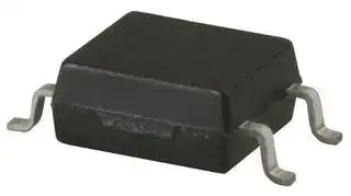
- Contact Form:SPST-NO (1 Form A); Load Type:AC / DC; Load Voltage Max:60V; Load Current:100mA; MOSFET Relay Package Style:SOP-4; Relay Mounting:Surface Mount; Relay 32M5997
| Delivery and price | |
|---|---|
| Units per pack | 4000 |
| Price | 0.475 € |
| Current stock | 10+ |
| Lead time | 7 days |
**VO1400AEF**

**==> picture [59 x 48] intentionally omitted <==**

www.vishay.com

## Vishay Semiconductors

## **1 Form A Solid-State Relay**

## **FEATURES**

**==> picture [226 x 85] intentionally omitted <==**

**----- Start of picture text -----**<br>
1 4<br>A S1<br>2<br>K 3<br>S2<br>i179066_6<br>**----- End of picture text -----**<br>


- Maximum RON 5 Ω

- Load voltage 60 V

- Load current 100 mA

- Isolation test voltage 3750 VRMS

- Small 4 pin SOP package

- Clean bounce free switching

- TTL / CMOS compatible input

- High reliability hybrid receptor

## **DESCRIPTION**

The VO1400AEF is an optically isolated 1 form A solid-state relay in a surface mount 4 pin SOP package.

## **APPLICATIONS**

- Security systems

- Instrumentation

- Industrial controls

- Available on tape and reel

- Material categorization: for definitions of compliance please see www.vishay.com/doc?99912

## **AGENCY APPROVALS**

- UL, file no. E52744

- cUL, file no. E52744

- DIN EN 60747-5-5 (VDE 0884-5)

- FIMKO EN 60950-1

- CQC GB8898-2011

## **ORDERING INFORMATION**

|**ORDERING INFORMATION**|**ORDERING INFORMATION**|**ORDERING INFORMATION**|**ORDERING INFORMATION**|**ORDERING INFORMATION**|
|---|---|---|---|---|
||||||
||**V**<br>**O**<br>**1**<br>**4**<br>**0**<br>**0**<br>**A**<br>**E**<br>**F**<br>PART NUMBER<br>ELECTRICAL<br>VARIATION<br>PACKAGE<br>CONFIG.||**T**|SOP|
|**PACKAGE**|||**UL, cUL, CQC, VDE, FIMKO**||
|SOP-4, tape and reel|||VO1400AEFTR||
|SOP-4, tape and reel (product rotated in tape)|||VO1400AEFT1||


|**ABSOLUTE MAXIMUM RATINGS**(Tamb= 25 °C,unless otherwise specified)|**ABSOLUTE MAXIMUM RATINGS**(Tamb= 25 °C,unless otherwise specified)|**ABSOLUTE MAXIMUM RATINGS**(Tamb= 25 °C,unless otherwise specified)|**ABSOLUTE MAXIMUM RATINGS**(Tamb= 25 °C,unless otherwise specified)|**ABSOLUTE MAXIMUM RATINGS**(Tamb= 25 °C,unless otherwise specified)|
|---|---|---|---|---|
|**PARAMETER**|**CONDITIONS**|**SYMBOL**|**VALUE**|**UNIT**|
|**INPUT**|||||
|LED continuous forward current||IF|50|mA|
|LED reverse voltage||VR|5|V|
|**OUTPUT**|||||
|DC or peak AC load voltage||VL|60|V|
|Load current AC peak||IL|100|mA|
|Peak load current|t = 10 ms|ILPK|350|mA|
|**SSR**|||||
|Total power dissipation||Pdiss|120|mW|
|Ambient temperature range||Tamb|-40 to +85|°C|
|Storage temperature range||Tstg|-40 to +125|°C|
|Soldering temperature|t≤10 s max.|Tsld|260|°C|


## **Notes**

- Stresses in excess of the absolute maximum ratings can cause permanent damage to the device. Functional operation of the device is not implied at these or any other conditions in excess of those given in the operational sections of this document. Exposure to absolute maximum ratings for extended periods of the time can adversely affect reliability.

Rev. 1.7, 14-Jul-15

Document Number: 84724

**1**

For technical questions, contact: optocoupleranswers@vishay.com THIS DOCUMENT IS SUBJECT TO CHANGE WITHOUT NOTICE. THE PRODUCTS DESCRIBED HEREIN AND THIS DOCUMENT ARE SUBJECT TO SPECIFIC DISCLAIMERS, SET FORTH AT www.vishay.com/doc?91000

**VO1400AEF**

**==> picture [59 x 48] intentionally omitted <==**

www.vishay.com

## Vishay Semiconductors

## **ABSOLUTE MAXIMUM RATING CURVE**

**==> picture [176 x 152] intentionally omitted <==**

**----- Start of picture text -----**<br>
160<br>140<br>120<br>100<br>80<br>60<br>40<br>20<br>0<br>-50 -25 0 25 50 75 100 125 150 175<br>Tamb - Ambient Temperature (°C)<br> - Input Safety Current (mA)<br>ISI<br>**----- End of picture text -----**<br>


**==> picture [176 x 152] intentionally omitted <==**

**----- Start of picture text -----**<br>
120<br>100<br>80<br>60<br>40<br>20<br>0<br>-40 -20 0 20 40 60 80 100<br>Tamb - Ambient Temperature (°C)<br> - Load Current (mA)IL<br>**----- End of picture text -----**<br>


Fig. 1 - Input Safety Current vs. Ambient Temperature

Fig. 3 - Load Current vs. Ambient Temperature

**==> picture [176 x 152] intentionally omitted <==**

**----- Start of picture text -----**<br>
500<br>400<br>300<br>200<br>100<br>0<br>-50 -25 0 25 50 75 100 125 150 175<br>Tamb - Ambient Temperature (°C)<br> - Output Safety Power (mW)<br>SO<br>P<br>**----- End of picture text -----**<br>


Fig. 2 - Output Safety Power vs. Ambient Temperature

|**ELECTRICAL CHARACTERISTICS**(Tamb= 25 °C,unless otherwise specified)|**ELECTRICAL CHARACTERISTICS**(Tamb= 25 °C,unless otherwise specified)|**ELECTRICAL CHARACTERISTICS**(Tamb= 25 °C,unless otherwise specified)|**ELECTRICAL CHARACTERISTICS**(Tamb= 25 °C,unless otherwise specified)|**ELECTRICAL CHARACTERISTICS**(Tamb= 25 °C,unless otherwise specified)|**ELECTRICAL CHARACTERISTICS**(Tamb= 25 °C,unless otherwise specified)|**ELECTRICAL CHARACTERISTICS**(Tamb= 25 °C,unless otherwise specified)|
|---|---|---|---|---|---|---|
|**PARAMETER**|**TEST CONDITION**|**SYMBOL**|**MIN.**|**TYP.**|**MAX.**|**UNIT**|
|**INPUT**|||||||
|LED forward current, switch turn-on|IL= 100 mA, VL ≤0.5 V, t = 10 ms|IFon|0.3|0.8|3.2|mA|
|LED forward current, switch turn-off|VL= 60 V|IFoff|100|400|-|μA|
|LED reverse current|VR= 5 V|IR|-|0.001|10|μA|
|LED forward voltage|IF= 5 mA|VF|0.8|1.1|1.4|V|
|LED reverse voltage|IR= 10 μA|VR|5|40||V|
|**OUTPUT**|||||||
|On-resistance|IF= 10 mA, IL= 100 mA|RON|-|2.3|5|Ω|
|Off-state leakage current|IF= 0 mA, VL= 60 V|ILEAK|-|0.002|1|μA|


## **Note**

- Minimum and maximum values are testing requirements. Typical values are characteristics of the device and are the result of engineering evaluations. Typical values are for information only and are not part of the testing requirements.

Rev. 1.7, 14-Jul-15

Document Number: 84724

**2**

For technical questions, contact: optocoupleranswers@vishay.com THIS DOCUMENT IS SUBJECT TO CHANGE WITHOUT NOTICE. THE PRODUCTS DESCRIBED HEREIN AND THIS DOCUMENT ARE SUBJECT TO SPECIFIC DISCLAIMERS, SET FORTH AT www.vishay.com/doc?91000

**VO1400AEF**

Vishay Semiconductors

**==> picture [59 x 48] intentionally omitted <==**

www.vishay.com

|**SWITCHING CHARACTERISTICS**|**SWITCHING CHARACTERISTICS**|**SWITCHING CHARACTERISTICS**|**SWITCHING CHARACTERISTICS**|**SWITCHING CHARACTERISTICS**|**SWITCHING CHARACTERISTICS**|**SWITCHING CHARACTERISTICS**|**SWITCHING CHARACTERISTICS**|**SWITCHING CHARACTERISTICS**||||
|---|---|---|---|---|---|---|---|---|---|---|---|
|**PARAMETER**||||**TEST CONDITION**|||**SYMBOL**|**MIN.**|**TYP.**|**MAX.**|**UNIT**|
|Turn-on time||IF||= 10 mA, VL= 20 V, IL= 100 mA|||ton|-|52|500|μs|
|Turn-off time||IF||= 10 mA, VL= 20 V, IL= 100 mA|||toff|-|36|500|μs|
|20991-2<br>Input<br>Output|||||||||Output<br>VL|||
||||||10 %<br>90 %<br>ton<br>toff<br>1.25 ms|||||||
||||||.|||||||
|||||||||||||
|||||||||||||
|||||||||||||
||||||10 %<br>90<br>ton<br>toff|||||||
|||||||||||||
|||||||||||||


Fig. 4 - Timing Test Circuit and Waveforms

|**SAFETY AND INSULATION RATINGS**|**SAFETY AND INSULATION RATINGS**||||
|---|---|---|---|---|
|**PARAMETER**|**TEST CONDITION**|**SYMBOL**|**VALUE**|**UNIT**|
|Climatic classification|Accordingto IEC 68 part 1||40/85/21||
|Pollution degree|Accordingto DIN VDE 0109||2||
|Comparative trackingindex|Insulationgroup IIIa|CTI|175||
|Maximum rated withstandingisolation voltage|Accordingto UL1577, t = 1 min|VISO|3750|VRMS|
|Maximum transient isolation voltage|Accordingto DIN EN 60747-5-5|VIOTM|6000|Vpeak|
|Maximum repetitive peak isolation voltage|Accordingto DIN EN 60747-5-5|VIORM|707|Vpeak|
|Insulation resistance|Tamb= 25 °C, VIO= 500 V|RIO|≥1012|Ω|
||Tamb= 100 °C, VIO= 500 V|RIO|≥1011|Ω|
||Tamb= TS, VIO= 500 V|RIO|≥109|Ω|
|Output safety power||PSO|400|mW|
|Input safety current||ISI|150|mA|
|Input safety temperature||TS|165|°C|
|Clearance distance|Measured from input terminals to output<br>terminals, shortest distance through air||≥5|mm|
|Creepage distance|Measured from input terminals to output<br>terminals, shortest distance path alongbody||≥5|mm|
|Input to output test voltage, method B|VIORMx 1.875 = VPR, 100 % production test<br>with tM= 1 s, partial discharge < 5 pC|VPR|1326|Vpeak|
|Input to output test voltage, method A|VIORMx 1.6 = VPR, 100 % sample test<br>with tM= 10 s, partial discharge < 5 pC|VPR|1131|Vpeak|


## **Note**

- This SSR is suitable for “safe electrical insulation” only within the safety ratings. Compliance with the safety ratings shall be ensured by means of protective circuits.

Rev. 1.7, 14-Jul-15

Document Number: 84724

**3**

For technical questions, contact: optocoupleranswers@vishay.com THIS DOCUMENT IS SUBJECT TO CHANGE WITHOUT NOTICE. THE PRODUCTS DESCRIBED HEREIN AND THIS DOCUMENT ARE SUBJECT TO SPECIFIC DISCLAIMERS, SET FORTH AT www.vishay.com/doc?91000

**VO1400AEF**

Vishay Semiconductors

**==> picture [59 x 48] intentionally omitted <==**

**==> picture [77 x 10] intentionally omitted <==**

**----- Start of picture text -----**<br>
www.vishay.com<br>**----- End of picture text -----**<br>


## **TYPICAL CHARACTERISTICS** (Tamb = 25 °C, unless otherwise specified)

**==> picture [176 x 152] intentionally omitted <==**

**----- Start of picture text -----**<br>
100<br>T = 85  ° C<br>T = 25 °C<br>10<br>T = -40 °C<br>1<br>0.6 0.8 1.0 1.2 1.4 1.6<br>VF - Forward Voltage (V)<br> - Forward Current (mA)<br>IF<br>**----- End of picture text -----**<br>


**==> picture [176 x 152] intentionally omitted <==**

**----- Start of picture text -----**<br>
0.020<br>VLOAD = 60 V<br>0.015<br>0.010<br>0.005<br>0<br>-40 -20 0 20 40 60 80 100<br>Tamb - Ambient Temperature (°C)<br> - Leakage Current (μA)<br>ILEAK<br>**----- End of picture text -----**<br>


Fig. 5 - Forward Current vs. Forward Voltage

Fig. 8 - Leakage Current vs. Ambient Temperature

**==> picture [184 x 154] intentionally omitted <==**

**----- Start of picture text -----**<br>
2.5<br>IL = 100 mA<br>2.0<br>1.5<br>1.0<br>0.5<br>0.0<br>-40  -20  0  20  40  60  80  100<br>Tamb - Ambient Temperature (°C)<br> - Forward Current forIFSwitch Turn-On (mA)<br>**----- End of picture text -----**<br>


**==> picture [175 x 152] intentionally omitted <==**

**----- Start of picture text -----**<br>
0.10<br>IL = 100 mA, tp = 5 ms<br>0.08<br>0.06<br>0.04<br>0.02<br>0<br>5 10 15 20<br>IF - Forward Current (mA)<br> - Turn-On Time (ms)<br>ton<br>**----- End of picture text -----**<br>


Fig. 6 - Forward Current for Switch Turn-On vs. Ambient Temperature

Fig. 9 - Turn-On Time vs. Forward Current

**==> picture [168 x 152] intentionally omitted <==**

**----- Start of picture text -----**<br>
6<br>IL = 100 mA<br>5<br>4  IF = 5 mA<br>3<br>2<br>IF = 10 mA<br>1<br>-40  -20  0  20  40  60  80  100<br>Tamb - Ambient Temperature (°C)<br>)Ω<br> - On-Resistance (<br>on<br>R<br>**----- End of picture text -----**<br>


**==> picture [175 x 152] intentionally omitted <==**

**----- Start of picture text -----**<br>
0.10<br>IL = 100 mA, tp = 5 ms<br>0.08<br>0.06<br>0.04<br>0.02<br>0<br>5 10 15 20<br>IF - Forward Current (mA)<br> - Turn-Off Time (ms)<br>toff<br>**----- End of picture text -----**<br>


Fig. 7 - On-Resistance vs. Ambient Temperature

Fig. 10 - Turn-Off Time vs. Forward Current

Rev. 1.7, 14-Jul-15

Document Number: 84724

**4**

For technical questions, contact: optocoupleranswers@vishay.com THIS DOCUMENT IS SUBJECT TO CHANGE WITHOUT NOTICE. THE PRODUCTS DESCRIBED HEREIN AND THIS DOCUMENT ARE SUBJECT TO SPECIFIC DISCLAIMERS, SET FORTH AT www.vishay.com/doc?91000

**VO1400AEF**

Vishay Semiconductors

**==> picture [59 x 48] intentionally omitted <==**

**==> picture [77 x 10] intentionally omitted <==**

**----- Start of picture text -----**<br>
www.vishay.com<br>**----- End of picture text -----**<br>


## **PACKAGE DIMENSIONS** (in millimeters)

**==> picture [425 x 138] intentionally omitted <==**

**----- Start of picture text -----**<br>
6.95 ± 0.25<br>4.92 max.<br>5.35 typ.<br>4.42 ± 0.25<br>4.57 ± 0.25<br>0.41 ± 0.10<br>0.50 ± 0.15 5.0 min. Leads coplanarity<br>0.1 max.<br>2.54 nom.<br>0.20 ± 0.10<br>2.12 ± 0.20<br>0.05 ± 0.05<br>**----- End of picture text -----**<br>


**==> picture [389 x 152] intentionally omitted <==**

**----- Start of picture text -----**<br>
4 3<br>Recommended footprint<br>Pin one I.D.<br>1.15 5.10<br>1 2<br>7.40<br>2.54<br>0.90<br>**----- End of picture text -----**<br>


Fig. 11 - Package Drawings

Rev. 1.7, 14-Jul-15

Document Number: 84724

**5**

For technical questions, contact: optocoupleranswers@vishay.com THIS DOCUMENT IS SUBJECT TO CHANGE WITHOUT NOTICE. THE PRODUCTS DESCRIBED HEREIN AND THIS DOCUMENT ARE SUBJECT TO SPECIFIC DISCLAIMERS, SET FORTH AT www.vishay.com/doc?91000

**VO1400AEF**

Vishay Semiconductors

**==> picture [59 x 48] intentionally omitted <==**

www.vishay.com

## **PACKAGE MARKING**

**==> picture [76 x 91] intentionally omitted <==**

**----- Start of picture text -----**<br>
1400<br>V YWW<br>68<br>Fig. 12 - VO1400AEF<br>**----- End of picture text -----**<br>


## **Note**

- Tape and reel suffix (TR) is not part of the package marking.

## **TAPE AND REEL INFORMATION** (in millimeters)

**==> picture [481 x 168] intentionally omitted <==**

**----- Start of picture text -----**<br>
2.0 ± 0.1 4.0 ± 0.1 1.5 ± 0.1<br>Pin 1 1.75 ± 0.1<br>0.35 ± 0.05<br>5.5 ± 0.1<br>12.0 ± 0.3<br>7.33 ± 0.1 7.33 ± 0.1 CL<br>8.0 ± 0.1 4.72 ± 0.1 1.5 ± 0.1<br>2.36 ± 0.1<br>2.66 ± 0.1<br>**----- End of picture text -----**<br>


**==> picture [19 x 6] intentionally omitted <==**

**----- Start of picture text -----**<br>
Note:<br>**----- End of picture text -----**<br>


- Cummulative tolerance of 10 spocket holes is 0.20

Fig. 13 - VO1400AEFT (2000 pieces on reel)

**==> picture [455 x 146] intentionally omitted <==**

**----- Start of picture text -----**<br>
Pin 1 2.0 ± 0.1 4.0 ± 0.1 1.5 ± 0.1 1.75 ± 0.1<br>0.32 ± 0.05<br>5.5 ± 0.1<br>12.0 ± 0.3<br>4.72 ± 0.1 4.72 ± 0.1 CL<br>2.36 ± 0.1<br>12.0 ± 0.1 7.33 ± 0.1<br>2.66 ± 0.1<br>1.5 ± 0.1<br>**----- End of picture text -----**<br>


**==> picture [19 x 6] intentionally omitted <==**

**----- Start of picture text -----**<br>
Note:<br>**----- End of picture text -----**<br>


- Cummulative tolerance of 10 spocket holes is 0.20

Fig. 14 - VO1400AEFT1 (1000 pieces on reel)

Rev. 1.7, 14-Jul-15

Document Number: 84724

**6**

For technical questions, contact: optocoupleranswers@vishay.com THIS DOCUMENT IS SUBJECT TO CHANGE WITHOUT NOTICE. THE PRODUCTS DESCRIBED HEREIN AND THIS DOCUMENT ARE SUBJECT TO SPECIFIC DISCLAIMERS, SET FORTH AT www.vishay.com/doc?91000

**VO1400AEF**

**==> picture [59 x 48] intentionally omitted <==**

www.vishay.com

## **SOLDER PROFILES**

**==> picture [172 x 151] intentionally omitted <==**

**----- Start of picture text -----**<br>
300<br>max. 260 °C<br>250 255 °C 245 °C<br>240 °C<br>217 °C<br>200<br>max. 30 s<br>150<br>max. 120 s max. 100 s<br>100<br>max. ramp down 6 °C/s<br>50 max. ramp up 3 °C/s<br>0<br>0 50 100 150 200 250 300<br>19841 Time (s)<br>Temperature (°C)<br>**----- End of picture text -----**<br>


## Vishay Semiconductors

## **HANDLING AND STORAGE CONDITIONS**

ESD level: HBM class 2 Floor life: unlimited Conditions: Tamb < 30 °C, RH < 85 % Moisture sensitivity level 1, according to J-STD-020

Fig. 15 - Lead (Pb)-free Reflow Solder Profile According to J-STD-020 for SMD Devices

Rev. 1.7, 14-Jul-15

Document Number: 84724

**7**

For technical questions, contact: optocoupleranswers@vishay.com THIS DOCUMENT IS SUBJECT TO CHANGE WITHOUT NOTICE. THE PRODUCTS DESCRIBED HEREIN AND THIS DOCUMENT ARE SUBJECT TO SPECIFIC DISCLAIMERS, SET FORTH AT www.vishay.com/doc?91000

**Legal Disclaimer Notice** Vishay

www.vishay.com

**==> picture [59 x 48] intentionally omitted <==**

## **Disclaimer**

ALL PRODUCT, PRODUCT SPECIFICATIONS AND DATA ARE SUBJECT TO CHANGE WITHOUT NOTICE TO IMPROVE RELIABILITY, FUNCTION OR DESIGN OR OTHERWISE.

Vishay Intertechnology, Inc., its affiliates, agents, and employees, and all persons acting on its or their behalf (collectively, “Vishay”), disclaim any and all liability for any errors, inaccuracies or incompleteness contained in any datasheet or in any other disclosure relating to any product.

Vishay makes no warranty, representation or guarantee regarding the suitability of the products for any particular purpose or the continuing production of any product.  To the maximum extent permitted by applicable law, Vishay disclaims (i) any and all liability arising out of the application or use of any product, (ii) any and all liability, including without limitation special, consequential or incidental damages, and (iii) any and all implied warranties, including warranties of fitness for particular purpose, non-infringement and merchantability.

Statements regarding the suitability of products for certain types of applications are based on Vishay’s knowledge of typical requirements that are often placed on Vishay products in generic applications.  Such statements are not binding statements about the suitability of products for a particular application.  It is the customer’s responsibility to validate that a particular product with the properties described in the product specification is suitable for use in a particular application. Parameters provided in datasheets and / or specifications may vary in different applications and performance may vary over time.  All operating parameters, including typical parameters, must be validated for each customer application by the customer’s technical experts.  Product specifications do not expand or otherwise modify Vishay’s terms and conditions of purchase, including but not limited to the warranty expressed therein.

Except as expressly indicated in writing, Vishay products are not designed for use in medical, life-saving, or life-sustaining applications or for any other application in which the failure of the Vishay product could result in personal injury or death. Customers using or selling Vishay products not expressly indicated for use in such applications do so at their own risk. Please contact authorized Vishay personnel to obtain written terms and conditions regarding products designed for such applications.

No license, express or implied, by estoppel or otherwise, to any intellectual property rights is granted by this document or by any conduct of Vishay.  Product names and markings noted herein may be trademarks of their respective owners.

Revision: 13-Jun-16

Document Number: 91000

**1**
Updated at March 23, 2026
Vishay is a global leader in the manufacturing of discrete semiconductors and passive electronic components. Renowned for its exceptional quality and engineering expertise, the company produces highly reliable solutions that drive innovation across the industrial, automotive, telecommunications, and consumer electronics markets. From advanced factory automation to vehicle electrification, Vishay components provide the foundational building blocks for modern electronic design. The company's expansive portfolio is heavily focused on efficient power management, signal routing, and energy storage. Within its passive component lineup, Vishay is recognized for its extensive array of high-performance capacitors, including robust aluminium electrolytic, film, and polymer variants, alongside highly efficient power inductors. In the realm of discrete semiconductors, Vishay is a premier manufacturer of single and dual MOSFETs, as well as a vast selection of Schottky, Zener, and fast-recovery rectifier diodes designed for demanding power applications. Furthermore, Vishay delivers industry-leading circuit protection and thermal management solutions. With a broad offering of transient voltage suppressors (TVS diodes) and temperature-sensing NTC thermistors, these components are engineered to safeguard sensitive circuitry against both electrical and thermal overstress. By combining this vital mix of advanced discretes and passives, Vishay enables engineers to develop robust, space-saving, and highly resilient electronic systems.
About Novapart
Novapart is a B2B electronic component broker specialising in stock shortages and cost reduction. We source hard-to-find parts and identify compliant alternatives across a catalogue of 540,000+ components from 500+ manufacturers.
Learn more →Stock Shortage Specialist
When a component is unavailable, discontinued or has an unacceptable lead time, we tap into our network of vetted European and Asian distributors to source what you need — without compromising on quality or traceability.
Request a quote →Compliant Alternatives
We identify pin-to-pin, electrically equivalent substitutes that meet the same certifications (RoHS, AEC-Q100, REACH) as your original specification — validated against datasheets, not just part numbers. Often at a lower cost.
BOM Analysis service →