
Image not available
Illustrative purposes only

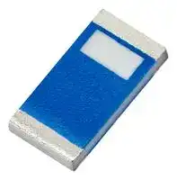
UWA.01
Chip Antenna, 7.9865 GHz/8.9855 GHz, 5.54dBi, 50 ohm, 2W, Linear
⚠️ Reference pricing provided. In case of supply shortages, we will connect you with our trusted procurement partners to ensure your project's continuity.
- Manufacturer: TAOGLAS
- Product type:
- Gain: 5.54dBi
- SVHC: To Be Advised
- VSWR: -
- Input Power: 2W
- Antenna Type: UWB
- Frequency Max: 9.235GHz
- Frequency Min: 8.736GHz
- Product Range: -
- Input Impedance: 50ohm
- Antenna Mounting: SMD
- Antenna Polarisation: Linear
| Delivery and price | |
|---|---|
| Units per pack | 500 |
| Price | 0.492 € |
| Current stock | 10+ |
| Lead time | 30 days |
Datasheet

AS ~ a“ > TAOGLAS.

+ 5 Qd on Y) (© +) (O C)

**Part No: UWA.01**

**Description**

6-9GHz UWB Ceramic Substrate Chip Antenna 3.2*1.6*0.5(mm)

**Features:**

Dimensions: 3.2mm *1.6mm * 0.5mm

High Efficiency 6-9GHz

Low profile Compact Size Surface-Mount RoHS and REACH compliant

SPE-23-8-017-A

www.taoglas.com

**==> picture [358 x 244] intentionally omitted <==**

**----- Start of picture text -----**<br>
1. Introduction  2<br>2. Specification  4<br>3. Antenna Characteristics  5<br>4. Radiation Patterns  9<br>5. Mechanical Drawing  16<br>6. Antenna Integration Guide  17<br>7. Solder Reflow Profile  24<br>8. Packaging  25<br>Changelog  26<br>**----- End of picture text -----**<br>


Taoglas makes no warranties based on the accuracy or completeness of the contents of this document and reserves the right to make changes to specifications and product descriptions at any time without notice. Taoglas reserves all rights to this document and the information contained herein. Reproduction, use or disclosure to third parties without express permission is strictly prohibited.

1

www.taoglas.com

SPE-23-8-017-A

Ultra-Wideband (also known as UWB) is a low power digital wireless technology for transmitting large amounts of digital data over a wide spectrum of frequency bands typically spanning more than 500MHz with very low power for short distances.

The low power requirements of UWB mean increased battery life of sensors and tags leading to reduction in overall operational costs. Taoglas has developed various innovative and new-to-market flexible embedded UWB antennas designed for seamless integration on plastics and using highly flexible micro-coaxial cable mounting while achieving high performance where space is limited. Taoglas UWB antennas have been designed for use with the recently launched UWB modules and are also compatible with any other UWB sensor modules on the market.

The UWA.01chip antenna, at 3.2mm *1.6mm * 0.5mm, is a small form factor Ultra-Wideband (UWB) antenna with high efficiencies across the pulsed UWB communications operational bands. It is mounted to a PCB via standard SMT reflow process. It enables designers to use only one antenna that covers most common UWB commercial bands, namely bands, 5 through 12 simultaneously.

Typical applications include:

- Indoor Tracking

- Warehousing and asset location

- Keyless entry and security

The UWA.01 antenna is a high efficiency, miniature SMD, edge mounted ceramic antenna that has a peak gain of more than 4dBi, an efficiency of more than 60% across the bands and is designed to be mounted directly onto a PCB. It is an ideal choice for any device maker that needs to keep manufacturing costs down over the lifetime of a product. Like all such antennas, care should be taken to mount the antenna at least 3mm from metal components or surfaces, and ideally 5mm for best Radiation efficiency.

The results below are based on a 80mm x 40mm ground-plane. If your ground-plane is smaller the efficiency will decrease, this can be tested in conjunction with Taoglas and we are happy to support customers integration. For more information please contact your regional Taoglas customer support team.

2

www.taoglas.com

SPE-23-8-017-A

## **1.1** Applications of Pulsed UWB antenna Technology

Radar-These short-pulsed antennas provide very fine range resolution and precision distance and positioning measurement capabilities. UWB signals enable inexpensive high definition radar antennas which find use in automotive sensors, smart airbags, and precision surveying applications amongst many others.

Home Network Connectivity- Smart home and entertainment systems can take advantage of high data rates for streaming high quality audio and video contents in real time for consumer electronics and computing within a home environment.

Position location & Tracking- UWB antennas also find use in Position Location and Tracking applications such as locating patients in case of critical condition, hikers injured in remote areas, tracking cars, and managing a variety of goods in a big shopping mall. UWB offers better noise immunity and better accuracy to within a few cm compared to current localization technologies such as Assisted GPS for Indoors, Wi-Fi and cellular which are at best able to offer meter level precision. Tethered Indoor positioning UWB systems that measure the angles of arrival of ultra-wideband (UWB) radio signals perform triangulation by using multiple sensors to communicate with a tag device.

3

www.taoglas.com

SPE-23-8-017-A

|**Electrical**|**Electrical**|**Electrical**|**Electrical**|**Electrical**|**Electrical**|**Electrical**|**Electrical**|**Electrical**|
|---|---|---|---|---|---|---|---|---|
|**Band**|Frequency<br>(MHz)|Efficiency (%)|Average Gain<br>(dB)|Peak Gain (dBi)|Peak Gain (dBi)<br>Impedance|Polarization|Radiation<br>Pattern|Max. input<br>power|
|**Channel 5**|6240-6739|84.3|-0.74|4.62|50 Ω|Linear|Omni|2W|
|**Channel 6**|6739-7238|81.7|-0.88|4.79|||||
|**Channel 7**|5948-7030|82.7|-0.82|4.66|||||
|**Channel 8**|7238-7737|89.6|-0.48|5.13|||||
|**Channel 9**|7737-8236|80.5|-0.94|4.47|||||
|**Channel 10**|8236-8736|74.3|-1.29|4.95|||||
|**Channel 11**|7321-8652|81.7|-0.88|5.13|||||
|**Channel 12**|8736-9235|71.5|-1.46|5.54|||||


*Results based on 80x40mm Evaluation Board

||**Mechanical**||
|---|---|---|
|Dimensions (mm)||3.2 x 1.6 x 0.5|
|Material||Ceramic|
|Weight (g)||0.02|
||||
||**Environmental**|**Environmental**|
|Temperature Range||-40°C to 105°C|
|Humidity||Non-condensing 65°C 95% RH|
|Moisture Sensitivity Level (MSL)||3 (168 Hours)|


4

www.taoglas.com

SPE-23-8-017-A

## Test Setup

5

www.taoglas.com

SPE-23-8-017-A

## Return Loss

## VSWR

6

www.taoglas.com

SPE-23-8-017-A

## **3.4** Efficiency es

**3.5** Average Gain es

7

www.taoglas.com

SPE-23-8-017-A

## Peak Gain

## Group Delay

8

www.taoglas.com

SPE-23-8-017-A

## Test Setup

9

www.taoglas.com

SPE-23-8-017-A

## UWA.01 Patterns at 6500 MHz

## XZ Plane

## YZ Plane

## XY Plane

10

www.taoglas.com

SPE-23-8-017-A

## UWA.01 Patterns at 7000 MHz

## XZ Plane

## YZ Plane

## XY Plane

11

www.taoglas.com

SPE-23-8-017-A

## UWA.01 Patterns at 7500 MHz

## XZ Plane

## YZ Plane

**==> picture [44 x 9] intentionally omitted <==**

**----- Start of picture text -----**<br>
XY Plane<br>**----- End of picture text -----**<br>


12

www.taoglas.com

SPE-23-8-017-A

## UWA.01 Patterns at 8000 MHz

## XZ Plane

## YZ Plane

## XY Plane

13

www.taoglas.com

SPE-23-8-017-A

## UWA.01 Patterns at 8500 MHz

## XZ Plane

## YZ Plane

## XY Plane

14

www.taoglas.com

SPE-23-8-017-A

## UWA.01 Patterns at 9000 MHz

## XZ Plane

## YZ Plane

## XY Plane

15

www.taoglas.com

SPE-23-8-017-A

16

www.taoglas.com

SPE-23-8-017-A

17

www.taoglas.com

SPE-23-8-017-A

## **6.1** Schematic and Symbol Definition |

The circuit symbol for the antenna is shown below. The antenna has 3 pins with only two pins as functional.

|**Pin**<br>~~a~~|**Description**|
|---|---|
|1|RF Feed|
|2|Mechanical, Not Connected|
|3|FTE (Fine Tuning Element)|


Please note you can download the design files, 3D model and 2D drawings files from the website here: https://www.taoglas.com/datasheets/UWA.01 .pdf

18

www.taoglas.com

SPE-23-8-017-A

## Antenna Integration

For any given PCB size, the antenna should ideally be placed at the centre edge of the PCB’s longest side, to take advantage of the ground plane.

## PCB Layout

The footprint and clearance on the PCB must meet the layout drawing in section (Footprint Drawing). Note the placement of the optimized components. R1 is placed as close as possible to the RF feed (pad 1) outside the copper keep out area. R2 is then placed tightly within the copper keep out area connected to RF Feed and the Fine-Tuning Element (pad 3). C1 & C2 are an optional components but the footprints are recommended in case they are needed.

19

www.taoglas.com

SPE-23-8-017-A

## PCB Keep out

Below shows the antenna footprint and clearance through ALL layers on the PCB. Only the antenna pads and connections to feed and GND are present within this clearance area (marked RED). The clearance area extends to 6mm in length and 7.5mm in width from the centre edge on the long side of the PCB. This clearance area includes the bottom side and ALL internal layers on the PCB.

20

www.taoglas.com

SPE-23-8-017-A

## Evaluation Board

**==> picture [355 x 101] intentionally omitted <==**

**----- Start of picture text -----**<br>
80mm<br>—m—m—m>0ssss®®0_0CwC00_0€—0—€—_0— EEE P—“i—iCT<br>° ejie ci c2® i ij e e ° C ° ® t C<br>¢ eeccooesen T—" 6<br>e = no ANTI ®<br>° aome eomeoeme88 kee8888808085507 +H4 ° e e °<br>: . Li . oe oo LJ<br>oo®<br>s<br>**----- End of picture text -----**<br>


21

www.taoglas.com

SPE-23-8-017-A

## **6.6** Evaluation Board Matching Circuit Ea

The UWA.01 doesn’t require any matching components on the Evaluation board, however, a ‘pi’ matching network is recommended if it is necessary for your device. A ‘O ohms’ link is applied in our Evaluation board. Another ‘O ohms’ (R2) is applied in the Fine Tune Element port (FTE) which can be changed later to fine tune the antenna.

|**Designator**|**Type**|**Value**|**Manufacturer**|**Manufacturer Part**<br>**Number**|
|---|---|---|---|---|
|R1|Resistor|0 Ohms|Yageo|RC0402JR-070RL|
|R2|Resistor|0 Ohms|Panasonic|ERJ-1GN0R00C|
|C1, C2|Capacitor|Not Fitted|-|-|


22

www.taoglas.com

SPE-23-8-017-A

## **6.7** Footprint ead

23

www.taoglas.com

SPE-23-8-017-A

Typical Soldering Profile for Lead-free Process:

24

www.taoglas.com

SPE-23-8-017-A

25

www.taoglas.com

SPE-23-8-017-A

Changelog for the datasheet

**SPE-23-8-017 - UWLA.01**

## **Revision: A (Original First Release)**

Date: 2023-01-30 Notes: Initial Release. Author: Gary West

## **Previous Revisions**

**==> picture [495 x 480] intentionally omitted <==**

26

www.taoglas.com

SPE-23-8-017-A

27

www.taoglas.com

SPE-23-8-017-A
Updated at June 9, 2026
About Novapart
Novapart is a B2B electronic component broker specialising in stock shortages and cost reduction. We source hard-to-find parts and identify compliant alternatives across a catalogue of 410,000+ components from 500+ manufacturers.
Learn more →Stock Shortage Specialist
When a component is unavailable, discontinued or has an unacceptable lead time, we tap into our network of vetted European and Asian distributors to source what you need — without compromising on quality or traceability.
Request a quote →Compliant Alternatives
We identify pin-to-pin, electrically equivalent substitutes that meet the same certifications (RoHS, AEC-Q100, REACH) as your original specification — validated against datasheets, not just part numbers. Often at a lower cost.
BOM Analysis service →