
Image not available
Illustrative purposes only

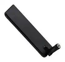
TG.30.8112
RF Antenna, 700 MHz to 2.7 GHz, Dipole, Linear, 5.3 dBi, SMA Connector Mount
⚠️ Reference pricing provided. In case of supply shortages, we will connect you with our trusted procurement partners to ensure your project's continuity.
- Manufacturer: TAOGLAS
- Product type:
- Gain: 5.3dBi
- SVHC: To Be Advised
- VSWR: -
- Input Power: 10W
- Antenna Type: Dipole
- Frequency Max: 2.7GHz
- Frequency Min: 700MHz
- Product Range: -
- Input Impedance: 50ohm
- Antenna Mounting: SMA Connector
- Antenna Polarisation: Linear
| Delivery and price | |
|---|---|
| Units per pack | 100 |
| Price | 19.12 € |
| Current stock | 10+ |
| Lead time | 30 days |
Datasheet

## **SPECIFICATION PATENTED**
Part No. : **TG.30.8112**
Product Name : Apex Black Right Angle TG.30 Ultra-Wideband 4G LTE Antenna
Feature
: LTE / GSM / CDMA /DCS /PCS / WCDMA / UMTS / HSDPA / GPRS / EDGE /GPS /Wi-Fi 698MHz to 960MHz, 1575.42MHz, 1710MHz to 2700Mhz Patented Typical 70%+ Efficiency and 3dBi+ Peak Gain Dipole Swivel Terminal Antenna 90° termination with SMA(M) Connector
**RoHS Compliant**
US Patent No.: 9559423 SPE-12-8-120/F/WY Page 1 of 21
## **1. Introduction**
The Apex Black Right Angle TG.30 Dipole LTE Antenna – is primarily designed for use with 4G LTE modules and devices that require the highest possible efficiency and peak gain to deliver best in class throughput on all major cellular (4G/3G/2G) bands worldwide for access points, terminals and routers. The antenna is a ground plane independent antenna with a SMA (M) connector and swivel mechanism that allows the antenna part to be rotated. The Apex exhibits high efficiency across the ultra wide band and is backward compatible with 3G and 2G cellular applications such as GSM, LTE, UMTS, Wi-Fi and even has GPS included for Assisted GPS and/or E911 applications. With very high efficiency on every cellular band globally it is an ideal solution for any device requiring high, reliable performance. It is also guaranteed to meet any type approval or carrier certification requirements from a RF standpoint. It is an omnidirectional antenna and the radiation patterns display this and are stable across all bands.
It has a quality robust housing for use with wireless terminals. The swivel mechanism allows the antenna part itself to be orientated in different directions and can help avoid touching off other antennas or objects close by as well as helping with isolation by orientating the antenna in different directions in MIMO systems for when other TG.30 antennas are present on the same device.
This patented antenna is also available in White and straight and right angle configurations.
US Patent No.: 9559423 SPE-12-8-120/F/WY Page 2 of 21
## **2. Specification**
|ELECTRICAL|ELECTRICAL|ELECTRICAL|ELECTRICAL|ELECTRICAL|ELECTRICAL|ELECTRICAL|ELECTRICAL|ELECTRICAL|
|---|---|---|---|---|---|---|---|---|
|Frequency (MHz)|700~800|700~800<br>824~960||824~960<br>1575.42|1575.42<br>1710 ~ 1880|1850 ~ 1990|1710 ~ 2170|2400~2700|
|Peak Gain (dBi)|||||||||
|Free Space|2.7|2.1||0.3|3.5|3.6|3.6|5.3|
|30x30cm GP center|30x30cm GP center<br>4.3|5.3||5.3|6.7|6.8|7.5|8.1|
|30x30cm GP edge|4.4|2.4||0.5|1.9|2.0|2.5|3.2|
|PCB edge|3.2|1.9||2.4|3.2|3.3|3.6|4.7|
|Average Gain|||||||||
|Free Space|-0.7|-1.2||-1.2|-0.4|-0.4|-0.2|-0.6|
|30x30cm GP center|30x30cm GP center<br>-2.8|-1.0||-2.4|-1.6|-1.8|-1.3|-1.2|
|30x30cm GP edge|-0.1|-4.3||-2.5|-2.0|-2.0|-2.0|-2.2|
|PCB edge|0.8|-1.9||-0.9|-0.6|-0.6|-0.6|-0.8|
|Efficiency|||||||||
|Free Space|85%|75%||76%|90%|90%|90%|87%|
|30x30cm GP center|30x30cm GP center<br>52%|39%||57%|70%|65%|74%|75%|
|30x30cm GP edge|91%|64%||56%|62%|62%|63%|60%|
|PCB edge|86%|87%||81%|86%|86%|86%|84%|
|Impedance|50Ω||||||||
|Polarization|Linear||||||||
|Radiation Pattern|Omni||||||||
|Input Power|10 W||||||||
|MECHANICAL|||||||||
|Casing|||UV Resistant PC/ABS||||||
|Connector|||SMA Male||||||
|ENVIRONMENTAL|||||||||
|Temperature Range|||-40°C to 85°C||||||
|Humidity|||Non-condensing 65°C 95% RH||||||
US Patent No.: 9559423 SPE-12-8-120/F/WY Page 3 of 21
|LTE BANDS<br>~~oo~~|LTE BANDS<br>~~oo~~|LTE BANDS<br>~~oo~~|LTE BANDS<br>~~oo~~|
|---|---|---|---|
|Band Number<br>~~oo~~|LTE/LTE-Advanced/WCDMA/HSPA/HSPA+/TD-SCDMA<br>~~oo~~|||
||**Uplink**|**Downlink**|**Covered**|
|**1**|UL: 1920 to 1980|DL: 2110 to 2170|✓|
|**2**|UL: 1850 to 1910|DL: 1930 to 1990|✓|
|**3**|UL: 1710 to 1785|DL: 1805 to 1880|✓|
|**4**|UL: 1710 to 1755|DL: 2110 to 2155|✓|
|**5**|UL: 824 to 849|DL: 869 to 894|✓|
|**7**|UL: 2500 to 2570|DL:2620 to 2690|✓|
|**8**|UL: 880 to 915|DL: 925 to 960|✓|
|**9**|UL: 1749.9 to 1784.9|DL: 1844.9 to 1879.9|✓|
|**11**|UL: 1427.9 to 1447.9|DL: 1475.9 to 1495.9||
|**12**|UL: 699 to 716|DL: 729 to 746|✓|
|**13**|UL: 777 to 787|DL: 746 to 756|✓|
|**14**|UL: 788 to 798|DL: 758 to 768|✓|
|**17**|UL: 704 to 716|DL: 734 to 746 (LTE only)|✓|
|**18**|UL: 815 to 830|DL: 860 to 875 (LET only)|✓|
|**19**|UL: 830 to 845|DL: 875 to 890|✓|
|**20**|UL: 832 to 862|DL: 791 to 821|✓|
|**21**|UL: 1447.9 to 1462.9|DL: 1495.9 to 1510.9||
|**22**|UL: 3410 to 3490|DL: 3510 to 3590||
|**23**|UL:2000 to 2020|DL: 2180 to 2200 (LTE only)|✓|
|**24**|UL:1625.5 to 1660.5|DL: 1525 to 1559 (LTE only)|✓|
|**25**|UL: 1850 to 1915|DL: 1930 to 1995|✓|
|**26**|UL: 814 to 849|DL: 859 to 894|✓|
|**27**|UL: 807 to 824|DL: 852 to 869 (LTE only)|✓|
|**28**|UL: 703 to 748|DL: 758 to 803 (LTE only)|✓|
|**29**|UL: -|DL: 717 to 728 (LTE only)|✓|
|**30**|UL: 2305 to 2315|DL: 2350 to 2360 (LTE only)|✓|
|**31**|UL: 452.5 to 457.5|DL: 462.5 to 467.5 (LTE only)||
|**32**|UL: -|DL: 1452 - 1496||
|**35**|1850 to 1910||✓|
|**38**|2570 to 2620||✓|
|**39**|1880 to 1920||✓|
|**40**|2300 to 2400||✓|
|**41**|2496 to 2690||✓|
|**42**|3400 to 3600|||
|**43**|3600 to 3800|||
*Covered bands represent an efficiency greater than 20%
US Patent No.: 9559423 SPE-12-8-120/F/WY Page 4 of 21
## **3. Antenna Characteristics**
## **3.1 Return Loss**
## **3.2 Peak Gain**
US Patent No.: 9559423 SPE-12-8-120/F/WY Page 5 of 21
## **3.3 Average Gain**
## **3.4 Efficiency**
US Patent No.: 9559423 SPE-12-8-120/F/WY Page 6 of 21
## **4. Antenna Radiation Patterns**
## **4.1 Antenna setup (Free Space)**
**==> picture [141 x 74] intentionally omitted <==**
**----- Start of picture text -----**<br>
Y<br>Z<br>X<br>**----- End of picture text -----**<br>
US Patent No.: 9559423 SPE-12-8-120/F/WY Page 7 of 21
## **4.2 Radiation Patterns (Free Space)**
XY Plane
**==> picture [13 x 9] intentionally omitted <==**
**----- Start of picture text -----**<br>
X<br>**----- End of picture text -----**<br>
**==> picture [13 x 9] intentionally omitted <==**
**----- Start of picture text -----**<br>
Y<br>**----- End of picture text -----**<br>
## X
**==> picture [13 x 10] intentionally omitted <==**
**----- Start of picture text -----**<br>
Y<br>**----- End of picture text -----**<br>
## X
**==> picture [13 x 10] intentionally omitted <==**
**----- Start of picture text -----**<br>
Y<br>**----- End of picture text -----**<br>
US Patent No.: 9559423 SPE-12-8-120/F/WY Page 8 of 21
## XZ Plane
**==> picture [377 x 359] intentionally omitted <==**
**----- Start of picture text -----**<br>
Z<br>0<br>10<br>330 30<br>300 Vi ‘ho \ 60<br>: -2 \ -<br>7 \o<br>270 i ag } 90 X<br>; —T04MHz<br>N —T751MHz<br>240 \‘ 120 —824MHz<br>SF —s8s0MHz<br>210 150<br>— oontie<br>180 (dBi)<br>Z Z<br>0 0<br>10<br>| 30 330 30<br>—<br>60 300 i‘4 10\ .\ 60<br>\ UA 2h \<br>) ; 90 X 270 ; / ; 830 ) 90 X<br>**----- End of picture text -----**<br>
US Patent No.: 9559423 SPE-12-8-120/F/WY Page 9 of 21
## **4.3 Antenna setup (On 300x300mm ground center)**
**==> picture [119 x 83] intentionally omitted <==**
**----- Start of picture text -----**<br>
Y<br>Z<br>X<br>**----- End of picture text -----**<br>
US Patent No.: 9559423 SPE-12-8-120/F/WY Page 10 of 21
**4.4 Radiation Patterns (On 300x300mm ground center)** XY Plane
**==> picture [14 x 10] intentionally omitted <==**
**----- Start of picture text -----**<br>
X<br>**----- End of picture text -----**<br>
**==> picture [13 x 10] intentionally omitted <==**
**----- Start of picture text -----**<br>
Y<br>**----- End of picture text -----**<br>
**==> picture [13 x 10] intentionally omitted <==**
**----- Start of picture text -----**<br>
X<br>**----- End of picture text -----**<br>
**==> picture [12 x 9] intentionally omitted <==**
**----- Start of picture text -----**<br>
Y<br>**----- End of picture text -----**<br>
**==> picture [13 x 10] intentionally omitted <==**
**----- Start of picture text -----**<br>
X<br>**----- End of picture text -----**<br>
**==> picture [12 x 9] intentionally omitted <==**
**----- Start of picture text -----**<br>
Y<br>**----- End of picture text -----**<br>
US Patent No.: 9559423 SPE-12-8-120/F/WY Page 11 of 21
## XZ Plane
**==> picture [376 x 362] intentionally omitted <==**
**----- Start of picture text -----**<br>
Z<br>0<br>10<br>Za<br>. / ~<br>270 33 | 90 X<br>_\ i _<br>\ } —751MHz<br>INS, ve<br>240 TAL A 120 _aoa IZ<br>f —8s0MHz<br>2101 \ \ 15)<br>° —960MHz<br>180 (aBi)<br>Z Z<br>0 0<br>3 ®<br>30 \ ZzZ 0 aN30<br>6 | av<br>) 60 300 }/; 2h ) 60<br>}— « 30 \) —<br>| 90 X \ | = | X<br>**----- End of picture text -----**<br>
US Patent No.: 9559423 SPE-12-8-120/F/WY Page 12 of 21
## **4.5 Antenna setup (On 300x300mm ground edge)**
**==> picture [118 x 82] intentionally omitted <==**
**----- Start of picture text -----**<br>
Y<br>Z<br>X<br>**----- End of picture text -----**<br>
US Patent No.: 9559423 SPE-12-8-120/F/WY Page 13 of 21
## **4.6 Radiation Patterns (On 300x300mm ground edge)**
## XY Plane
**==> picture [14 x 9] intentionally omitted <==**
**----- Start of picture text -----**<br>
X<br>**----- End of picture text -----**<br>
**==> picture [13 x 10] intentionally omitted <==**
**----- Start of picture text -----**<br>
Y<br>**----- End of picture text -----**<br>
**==> picture [13 x 10] intentionally omitted <==**
**----- Start of picture text -----**<br>
X<br>**----- End of picture text -----**<br>
**==> picture [14 x 10] intentionally omitted <==**
**----- Start of picture text -----**<br>
X<br>**----- End of picture text -----**<br>
**==> picture [265 x 11] intentionally omitted <==**
**----- Start of picture text -----**<br>
Y 270 { -40 | | 90 Y<br>**----- End of picture text -----**<br>
US Patent No.: 9559423 SPE-12-8-120/F/WY Page 14 of 21
## XZ Plane
**==> picture [389 x 374] intentionally omitted <==**
**----- Start of picture text -----**<br>
Z<br>0<br>10<br>330 \ | 30<br>\ 0 |<br>Zn. x<br>270 4 90 X<br>= K { : —704MHz<br>240 \ / —751MHz<br>Nei—— 120 —8g0MHz—824MHz<br>2101 15 ° —960MHz<br>180 (dBi)<br>Z<br>Z<br>0 )<br>10.<br>/ 30 330 30<br>= —~—— —<br>. ‘No<br>, 60 300 \ 60<br>\ f aA<br>} 90 X 270 | aE 90<br>iih i —2300MHz X<br>**----- End of picture text -----**<br>
US Patent No.: 9559423 SPE-12-8-120/F/WY Page 15 of 21
## **4.7 Antenna setup (On Ground Plane edge)**
**==> picture [116 x 83] intentionally omitted <==**
**----- Start of picture text -----**<br>
Y<br>Z<br>X<br>**----- End of picture text -----**<br>
US Patent No.: 9559423 SPE-12-8-120/F/WY Page 16 of 21
**4.8 Radiation Patterns (On Ground Plane edge)** XY Plane
**==> picture [14 x 9] intentionally omitted <==**
**----- Start of picture text -----**<br>
X<br>**----- End of picture text -----**<br>
**==> picture [13 x 10] intentionally omitted <==**
**----- Start of picture text -----**<br>
Y<br>**----- End of picture text -----**<br>
**==> picture [14 x 9] intentionally omitted <==**
**----- Start of picture text -----**<br>
X<br>**----- End of picture text -----**<br>
**==> picture [13 x 10] intentionally omitted <==**
**----- Start of picture text -----**<br>
Y<br>**----- End of picture text -----**<br>
**==> picture [13 x 10] intentionally omitted <==**
**----- Start of picture text -----**<br>
X<br>**----- End of picture text -----**<br>
**==> picture [12 x 10] intentionally omitted <==**
**----- Start of picture text -----**<br>
Y<br>**----- End of picture text -----**<br>
US Patent No.: 9559423 SPE-12-8-120/F/WY Page 17 of 21
## XZ Plane
**==> picture [392 x 382] intentionally omitted <==**
**----- Start of picture text -----**<br>
Z<br>0<br>10<br>300 i \ 60<br>f \<br>270 { | 90 X<br>; \ : —104MHz<br>—751MHz<br>240 120<br>—824MHz<br>—— — 880MHz<br>a1 15 ° —960MHz<br>180 (dBi)<br>Z Z<br>0 0<br>10.<br>30 330 30<br>—=—=— a<br>Lm N<br>60 300 Ve \ \ 60<br>/// 2cry| \x<br>| 90 X 270 \ => — 90 X<br>| \ / —2300MHz<br>**----- End of picture text -----**<br>
US Patent No.: 9559423 SPE-12-8-120/F/WY Page 18 of 21
## **5. Drawing**
US Patent No.: 9559423 SPE-12-8-120/F/WY Page 19 of 21
## **6. Packaging**
US Patent No.: 9559423 SPE-12-8-120/F/WY Page 20 of 21
Taoglas makes no warranties based on the accuracy or completeness of the contents of this document and reserves the right to make changes to specifications and product descriptions at any time without notice. Taoglas reserves all rights to this document and the information contained herein.
Reproduction, use or disclosure to third parties without express permission is strictly prohibited.
Copyright © Taoglas Ltd.
US Patent No.: 9559423 SPE-12-8-120/F/WY Page 21 of 21
Updated at June 9, 2026
About Novapart
Novapart is a B2B electronic component broker specialising in stock shortages and cost reduction. We source hard-to-find parts and identify compliant alternatives across a catalogue of 410,000+ components from 500+ manufacturers.
Learn more →Stock Shortage Specialist
When a component is unavailable, discontinued or has an unacceptable lead time, we tap into our network of vetted European and Asian distributors to source what you need — without compromising on quality or traceability.
Request a quote →Compliant Alternatives
We identify pin-to-pin, electrically equivalent substitutes that meet the same certifications (RoHS, AEC-Q100, REACH) as your original specification — validated against datasheets, not just part numbers. Often at a lower cost.
BOM Analysis service →