


TA6L33AHM3/H
TVS Diode, PAR eSMP, Unidirectional, 28.2 V, 45.7 V, DO-221AD, 2 Pins
- Manufacturer: VISHAY
- Product type: TVS Diodes
- Product Range:PAR eSMP Series; TVS Polarity:Unidirectional; Reverse Stand-Off Voltage Vrwm:28.2V; Clamping Voltage Vc Max:45.7V; Diode Case Style:DO-221AD; No. of Pins:2Pins; Breakdown
- SVHC: Lead (04-Feb-2026)
- No. of Pins: 2Pins
- TVS Polarity: Unidirectional
- Product Range: PAR eSMP
- Qualification: AEC-Q101
- Diode Mounting: Surface Mount
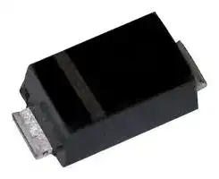
- Diode Case Style: DO-221AD
- Clamping Voltage Max: 45.7V
- Reverse Standoff Voltage: 28.2V
- Maximum Breakdown Voltage: 34.7V
- Minimum Breakdown Voltage: 31.4V
- Operating Temperature Max: 185°C
- Peak Pulse Power Dissipation: 600W
| Delivery and price | |
|---|---|
| Units per pack | 1000 |
| Price | 0.121 € |
| Current stock | 1000+ |
| Lead time | 30 days |
## **TA6L6.8A thru TA6L100A** www.vishay.com Vishay General Semiconductor a ~~a~~ **Surface Mount PAR[®] Transient Voltage Suppressors**

High Temperature Stability and High Reliability Conditions

**==> picture [70 x 10] intentionally omitted <==**

**----- Start of picture text -----**<br>
eSMP [® ] Series<br>**----- End of picture text -----**<br>


## **FEATURES**

- Low-profile package

**==> picture [20 x 4] intentionally omitted <==**

**----- Start of picture text -----**<br>
Available<br>**----- End of picture text -----**<br>


- Meets MSL level 1, per J-STD-020, LF maximum peak of 260 °C

- Junction passivation optimized design passivated anisotropic rectifier technology

- TJ = 185 °C capability suitable for high reliability and automotive requirement

- Excellent clamping capability

**==> picture [122 x 7] intentionally omitted <==**

**----- Start of picture text -----**<br>
Top View Bottom View<br>**----- End of picture text -----**<br>


## **SlimSMAW (DO-221AD)**

Cathode Anode

- Peak pulse power: 600 W (10 μs/1000 μs)

- AEC-Q101 qualified available, HM3 suffix meets JESD 201 class 2 whisker test

- ESD protection up to 30 kV per IEC 61000-4-2

- Compatible to SOD-128 package case outline

**LINKS TO ADDITIONAL RESOURCES** 3D Models Related Packages Marking ~~Be~~ Documents ~~A~~

## **PRIMARY CHARACTERISTICS**

|**PRIMARY CHARACTERISTICS**|**PRIMARY CHARACTERISTICS**|
|---|---|
|VBR|6.8 V to 100 V|
|VWM|5.8 V to 85.5 V|
|PPPM(10 x 1000 μs)|600 W|
|TJmax.|185 °C|
|Polarity|Unidirectional|
|Package|SlimSMAW (DO-221AD)|
|Circuit configuration|Single|


- Material categorization: for definitions of compliance please see www.vishay.com/doc?99912

- **TYPICAL APPLICATIONS** OC

## **TYPICAL APPLICATIONS**

Use in sensitive electronics protection against voltage transients induced by inductive load switching and lightning on ICs, MOSFET, signal lines of sensor units for automotive.

## **MECHANICAL DATA**

**Case:** SlimSMAW (DO-221AD)

Molding compound meets UL 94 V-0 flammability rating

Base P/NHM3 - halogen-free, RoHS-compliant, and AEC-Q101 qualified

**Terminals:** matte tin plated leads, solderable per J-STD-002 and JESD 22-B102

**Polarity:** color band denotes cathode end

|**MAXIMUM RATINGS**(TA= 25 °C,unless otherwise noted)|**MAXIMUM RATINGS**(TA= 25 °C,unless otherwise noted)|**MAXIMUM RATINGS**(TA= 25 °C,unless otherwise noted)|**MAXIMUM RATINGS**(TA= 25 °C,unless otherwise noted)|**MAXIMUM RATINGS**(TA= 25 °C,unless otherwise noted)|
|---|---|---|---|---|
|**PARAMETER**||**SYMBOL**|**VALUE**|**UNIT**|
|Peak pulse power dissipation<br>with a 10/1000 μs waveform||PPPM|600|W|
|Peak pulse current<br>with a 10/1000 μs waveform||IPPM|See table next page|A|
|Power dissipation|TM= 65 °C|PD(2)|8|W|
||TA= 25 °C|PD(3)|1.1||
|Operatingjunction and storage temperature range||TJ, TSTG|-65 to +185|°C|


## **Note**

> (1) Non-repetitive current pulse, per fig. 3 and derated above TA = 25 °C per fig. 2

- (2) Power dissipation mounted on infinite heat sink

- (3) Power dissipation mounted on minimum recommended pad layout

Revision: 16-Jan-2025

Document Number: 87415

**1**

For technical questions within your region: DiodesAmericas@vishay.com, DiodesAsia@vishay.com, DiodesEurope@vishay.com THIS DOCUMENT IS SUBJECT TO CHANGE WITHOUT NOTICE. THE PRODUCTS DESCRIBED HEREIN AND THIS DOCUMENT ARE SUBJECT TO SPECIFIC DISCLAIMERS, SET FORTH AT www.vishay.com/doc?91000

**TA6L6.8A thru TA6L100A**

www.vishay.com

## Vishay General Semiconductor

|**ELECTRICAL CHARACTERISTICS**(TA= 25 °C,unless otherwise noted)|**ELECTRICAL CHARACTERISTICS**(TA= 25 °C,unless otherwise noted)|**ELECTRICAL CHARACTERISTICS**(TA= 25 °C,unless otherwise noted)|**ELECTRICAL CHARACTERISTICS**(TA= 25 °C,unless otherwise noted)|**ELECTRICAL CHARACTERISTICS**(TA= 25 °C,unless otherwise noted)|**ELECTRICAL CHARACTERISTICS**(TA= 25 °C,unless otherwise noted)|**ELECTRICAL CHARACTERISTICS**(TA= 25 °C,unless otherwise noted)|**ELECTRICAL CHARACTERISTICS**(TA= 25 °C,unless otherwise noted)|**ELECTRICAL CHARACTERISTICS**(TA= 25 °C,unless otherwise noted)|**ELECTRICAL CHARACTERISTICS**(TA= 25 °C,unless otherwise noted)|**ELECTRICAL CHARACTERISTICS**(TA= 25 °C,unless otherwise noted)|**ELECTRICAL CHARACTERISTICS**(TA= 25 °C,unless otherwise noted)|
|---|---|---|---|---|---|---|---|---|---|---|---|
|**DEVICE**<br>**TYPE**|**DEVICE**<br>**MARKING**<br>**CODE**|**BREAKDOWN**<br>**VOLTAGE**<br>**VBR (1) AT IT **<br>**(V)**|||**TEST**<br>**CURRENT**<br>**IT **<br>**(mA)**|**STAND-**<br>**OFF**<br>**VOLTAGE**<br>**VWM**<br>**(V)**|**MAXIMUM**<br>**REVERSE**<br>**LEAKAGE**<br>**AT VWM**<br>**IR **<br>**(μA)**|**MAXIMUM**<br>**REVERSE**<br>**LEAKAGE**<br>**AT VWM**<br>**TJ = 150 °C**<br>**ID**<br>**(μA)**|**MAXIMUM**<br>**PEAK PULSE**<br>**SURGE**<br>**CURRENT**<br>**IPPM (2)**<br>**(A)**|**MAXIMUM**<br>**CLAMPING**<br>**VOLTAGE**<br>**AT IPPM**<br> **VC **<br>**(V)**|**TYPICAL**<br>**TEMP.**<br>**COEFFICIENT**<br>**OF VBR (3)**<br>α**T**<br>**(%/°C)**|
|||**MIN.**|**NOM.**|**MAX.**||||||||
|TA6L6.8A|AEL|6.45|6.80|7.14|10|5.80|500|1000|57.1|10.5|0.047|
|TA6L7.5A|AGL|7.13|7.50|7.88|10|6.40|250|500|53.1|11.3|0.052|
|TA6L8.2A|AKL|7.79|8.20|8.61|10|7.02|100|200|49.6|12.1|0.056|
|TA6L9.1A|AML|8.65|9.10|9.55|1.0|7.78|25|50|44.8|13.4|0.060|
|TA6L10A|APL|9.5|10.0|10.5|1.0|8.55|5.0|20|41.4|14.5|0.064|
|TA6L11A|ARL|10.5|11.0|11.6|1.0|9.40|2.0|5.0|38.5|15.6|0.067|
|TA6L12A|ATL|11.4|12.0|12.6|1.0|10.2|2.0|5.0|35.9|16.7|0.070|
|TA6L13A|AVL|12.4|13.0|13.7|1.0|11.1|2.0|5.0|33.0|18.2|0.072|
|TA6L15A|AXL|14.3|15.0|15.8|1.0|12.8|1.0|5.0|28.3|21.2|0.076|
|TA6L16A|AZL|15.2|16.0|16.8|1.0|13.6|1.0|5.0|26.7|22.5|0.078|
|TA6L18A|BEL|17.1|18.0|18.9|1.0|15.3|1.0|5.0|23.5|25.5|0.080|
|TA6L20A|BGL|19.0|20.0|21.0|1.0|17.1|1.0|5.0|21.7|27.7|0.082|
|TA6L22A|BKL|20.9|22.0|23.1|1.0|18.8|1.0|5.0|19.6|30.6|0.084|
|TA6L24A|BML|22.8|24.0|25.2|1.0|20.5|1.0|5.0|18.1|33.2|0.085|
|TA6L27A|BPL|25.7|27.0|28.4|1.0|23.1|1.0|5.0|16.0|37.5|0.087|
|TA6L30A|BRL|28.5|30.0|31.5|1.0|25.6|1.0|5.0|14.5|41.4|0.088|
|TA6L33A|BTL|31.4|33.0|34.7|1.0|28.2|1.0|5.0|13.1|45.7|0.089|
|TA6L36A|BVL|34.2|36.0|37.8|1.0|30.8|1.0|5.0|12.0|49.9|0.090|
|TA6L39A|BXL|37.1|39.0|41.0|1.0|33.3|1.0|5.0|11.1|53.9|0.091|
|TA6L43A|BZL|40.9|43.0|45.2|1.0|36.8|1.0|5.0|10.1|59.3|0.092|
|TA6L47A|CEL|44.7|47.0|49.4|1.0|40.2|1.0|5.0|9.3|64.8|0.092|
|TA6L51A|CGL|48.5|51.0|53.6|1.0|43.6|1.0|5.0|8.6|70.1|0.093|
|TA6L56A|CKL|53.2|56.0|58.8|1.0|47.8|1.0|10.0|7.8|77.0|0.096|
|TA6L62A|CML|58.9|62.0|65.1|1.0|53.0|1.0|10.0|7.1|85.0|0.096|
|TA6L68A|CPL|64.6|68.0|71.4|1.0|58.1|1.0|10.0|6.5|92.0|0.097|
|TA6L75A|CRL|71.3|75.0|78.8|1.0|64.1|1.0|10.0|5.8|104|0.097|
|TA6L82A|CTL|77.9|82.0|86.1|1.0|70.1|1.0|10.0|5.3|113|0.097|
|TA6L91A|CVL|86.5|91.0|95.6|1.0|77.8|1.0|15.0|4.8|125|0.098|
|TA6L100A|CXL|95.0|100|105|1.0|85.5|1.0|15.0|4.4|137|0.098|


## **Notes**

> (1) Pulse test: tp ≤ 50 ms

> (2) Surge current waveform per fig. 3 and derated per fig. 2

> (3) To calculate VBR vs. junction temperature, use the following formula: VBR at TJ = VBR at 25 °C x (1 + αT x (TJ - 25))

> (4) All terms and symbols are consistent with ANSI/IEEE C62.35

|**THERMAL CHARACTERISTICS**(TA= 25 °C unless otherwise noted)|**THERMAL CHARACTERISTICS**(TA= 25 °C unless otherwise noted)|**THERMAL CHARACTERISTICS**(TA= 25 °C unless otherwise noted)|**THERMAL CHARACTERISTICS**(TA= 25 °C unless otherwise noted)|**THERMAL CHARACTERISTICS**(TA= 25 °C unless otherwise noted)|
|---|---|---|---|---|
|**PARAMETER**|**SYMBOL**|**TYP.**|**MAX.**|**UNIT**|
|Thermal resistance|RθJA(1)|120|150|°C/W|
||RθJM (2)|12|15|°C/W|


## **Notes**

> (1) Thermal resistance junction-to-ambient to follow JEDEC® 51-2A,device mounted on FR4 PCB, 2 oz. standard footprint

> (2) Thermal resistance junction-to-mount to follow JEDEC® 51-14 using Transient Dual Interface Test Method (TDIM)

Revision: 16-Jan-2025

Document Number: 87415

**2**

For technical questions within your region: DiodesAmericas@vishay.com, DiodesAsia@vishay.com, DiodesEurope@vishay.com THIS DOCUMENT IS SUBJECT TO CHANGE WITHOUT NOTICE. THE PRODUCTS DESCRIBED HEREIN AND THIS DOCUMENT ARE SUBJECT TO SPECIFIC DISCLAIMERS, SET FORTH AT www.vishay.com/doc?91000

**TA6L6.8A thru TA6L100A**

www.vishay.com

Vishay General Semiconductor

|**IMMUNITY TO STATIC ELECTRICAL DISCHARGE TO THE FOLLOWING STANDARDS**<br>(TA= 25 °C unless otherwise noted)|**IMMUNITY TO STATIC ELECTRICAL DISCHARGE TO THE FOLLOWING STANDARDS**<br>(TA= 25 °C unless otherwise noted)|**IMMUNITY TO STATIC ELECTRICAL DISCHARGE TO THE FOLLOWING STANDARDS**<br>(TA= 25 °C unless otherwise noted)|**IMMUNITY TO STATIC ELECTRICAL DISCHARGE TO THE FOLLOWING STANDARDS**<br>(TA= 25 °C unless otherwise noted)|**IMMUNITY TO STATIC ELECTRICAL DISCHARGE TO THE FOLLOWING STANDARDS**<br>(TA= 25 °C unless otherwise noted)|
|---|---|---|---|---|
|**STANDARD**|**TEST TYPE**|**TEST CONDITIONS**|**SYMBOL**|**VALUE**|
|IEC 61000-4-2|Contact discharge|C = 150 pF, R = 330Ω|ESD|30 kV|
||Air discharge|||30 kV|


## **ORDERING INFORMATION** (Example)

|**ORDERING INFORMATION**(Example)|**ORDERING INFORMATION**(Example)|**ORDERING INFORMATION**(Example)|**ORDERING INFORMATION**(Example)|**ORDERING INFORMATION**(Example)|
|---|---|---|---|---|
|**PREFERRED P/N**|**UNIT WEIGHT (g)**|**PREFERRED PACKAGE CODE**|**BASE QUANTITY**|**DELIVERY MODE**|
|TA6L6.8AHM3/H(1)|0.033|H|3500|7" diameter plastic tape and reel|
|TA6L6.8AHM3/I(1)|0.033|I|14 000|13" diameter plastic tape and reel|


## **Note**

> (1) AEC-Q101 qualified

## **RATINGS AND CHARACTERISTICS CURVES** (TA = 25 °C, unless otherwise noted)

**==> picture [210 x 371] intentionally omitted <==**

**----- Start of picture text -----**<br>
10 10000<br>1000<br>TA6L6.8A thru<br>TA6L51A<br>1<br>100<br>TA6L56A thru<br>TA6L100A<br>0.1 10<br>10 100 1000 10000<br>td - Pulse Width (µs)<br>Fig. 1 - Peak Pulse Power Rating Curve<br>Axis Title<br>100 10000<br>Typical<br>80<br>1000<br>60<br>40<br>Safety operation area 100<br>20<br>0 10<br>0 25 50 75 100 125 150 175 200<br>TJ - Initial Temperature (°C)<br> - Peak Pulse Power (kW)<br>PPM<br>P<br>Derating in Percentage (%)<br>**----- End of picture text -----**<br>


Fig. 2 - Pulse Power or Current vs. Initial Junction Temperature

**==> picture [210 x 371] intentionally omitted <==**

**----- Start of picture text -----**<br>
150 10000<br>t r  = 10 µs TJ = 25  ° C<br>Pulse width (t d ) is defined<br>as the point where the peak<br>current decays to 50 % of IPPM<br>100 1000<br>Peak value I PPM<br>Half value IPPM - IPPM/2<br>50 100<br>10/1000 µs waveform<br>t d<br>0 10<br>0 0.5 1.0 1.5 2.0 2.5 3.0 3.5 4.0<br>tp - Time (ms)<br>Fig. 3 - Pulse Waveform<br>Axis Title<br>10 000 10000<br>T J  = 25  ° C,<br>f = 1.0 MHz,<br>V sig = 50 mV p-p<br>1000 1000<br>Measured at zero bias<br>100 100<br>Measured at stand-off<br>voltage, VWM<br>10 10<br>0 10 20 30 40 50 60 70 80 90 100<br>VBR - Breakdown Voltage (V)<br>RSM<br>- Peak Pulse Current, % I<br>IPPM<br>C - Junction Capacitance (pF)J<br>**----- End of picture text -----**<br>


**==> picture [134 x 9] intentionally omitted <==**

**----- Start of picture text -----**<br>
Fig. 4 - Typical Junction Capacitance<br>**----- End of picture text -----**<br>


Revision: 16-Jan-2025

Document Number: 87415

**3** For technical questions within your region: DiodesAmericas@vishay.com, DiodesAsia@vishay.com, DiodesEurope@vishay.com THIS DOCUMENT IS SUBJECT TO CHANGE WITHOUT NOTICE. THE PRODUCTS DESCRIBED HEREIN AND THIS DOCUMENT ARE SUBJECT TO SPECIFIC DISCLAIMERS, SET FORTH AT www.vishay.com/doc?91000

**TA6L6.8A thru TA6L100A**

## www.vishay.com

Vishay General Semiconductor

**==> picture [476 x 176] intentionally omitted <==**

**----- Start of picture text -----**<br>
9 10000 1000 10000<br>Junction to ambient<br>8<br>TA= TM, mounted on<br>7 infinite heatsink<br>6 1000 100 1000<br>5<br>4<br>3 100 10 100<br>2 FR-4 board, on minimum<br>recommended pad layout<br>1<br>0 10 1 10<br>0 25 50 75 100 125 150 175 200 0.01 0.1 1 10 100 1000<br>TA - Ambient Temperature (°C) t - Pulse Duration (s)<br>Fig. 5 - Power Dissipation Derating Curve Fig. 6 - Typical Transient Thermal Impedance<br>1st line 2nd line 2nd line2nd line<br> - Power Dissipation (W)<br>D<br>P<br>Transient Thermal Impedance (°C/W)<br>**----- End of picture text -----**<br>


## **Note**

- Fig. 1, power calculations is based on IPPM times defined maximum clamping voltage by pulse width

## **PACKAGE OUTLINE DIMENSIONS** in inches (millimeters)

## **SlimSMAW (DO-221AD)**

**==> picture [482 x 269] intentionally omitted <==**

**----- Start of picture text -----**<br>
Cathode band<br>0.106 (2.70) 0.075 (1.90)<br>0.091 (2.30) 0.063 (1.60)<br>0.158 (4.00) 0.032 (0.81) 0.024 (0.60)<br>0.014 (0.36) 0.012 (0.30)<br>0.142 (3.60)<br>0.197 (5.00)<br>0.173 (4.40)<br>0.043 (1.10)<br>0.035 (0.90)<br>0.083 (2.10) min.<br>0.009 (0.22)<br>0.004 (0.10)<br>0.118 (3.00) max.<br>0.055 (1.40) min. 0.055 (1.40) min.<br>0.228 (5.80) ref.<br>Mounting pad layout<br>**----- End of picture text -----**<br>


Revision: 16-Jan-2025

Document Number: 87415

**4**

For technical questions within your region: DiodesAmericas@vishay.com, DiodesAsia@vishay.com, DiodesEurope@vishay.com THIS DOCUMENT IS SUBJECT TO CHANGE WITHOUT NOTICE. THE PRODUCTS DESCRIBED HEREIN AND THIS DOCUMENT ARE SUBJECT TO SPECIFIC DISCLAIMERS, SET FORTH AT www.vishay.com/doc?91000

**Legal Disclaimer Notice** Vishay

www.vishay.com

## **Disclaimer**

ALL PRODUCT, PRODUCT SPECIFICATIONS AND DATA ARE SUBJECT TO CHANGE WITHOUT NOTICE TO IMPROVE RELIABILITY, FUNCTION OR DESIGN OR OTHERWISE.

Vishay Intertechnology, Inc., its affiliates, agents, and employees, and all persons acting on its or their behalf (collectively, “Vishay”), disclaim any and all liability for any errors, inaccuracies or incompleteness contained in any datasheet or in any other disclosure relating to any product.

Vishay makes no warranty, representation or guarantee regarding the suitability of the products for any particular purpose or the continuing production of any product. To the maximum extent permitted by applicable law, Vishay disclaims (i) any and all liability arising out of the application or use of any product, (ii) any and all liability, including without limitation special, consequential or incidental damages, and (iii) any and all implied warranties, including warranties of fitness for particular purpose, non-infringement and merchantability.

Statements regarding the suitability of products for certain types of applications are based on Vishay's knowledge of typical requirements that are often placed on Vishay products in generic applications. Such statements are not binding statements about the suitability of products for a particular application. It is the customer's responsibility to validate that a particular product with the properties described in the product specification is suitable for use in a particular application. Parameters provided in datasheets and / or specifications may vary in different applications and performance may vary over time. All operating parameters, including typical parameters, must be validated for each customer application by the customer's technical experts. Product specifications do not expand or otherwise modify Vishay's terms and conditions of purchase, including but not limited to the warranty expressed therein.

Hyperlinks included in this datasheet may direct users to third-party websites. These links are provided as a convenience and for informational purposes only. Inclusion of these hyperlinks does not constitute an endorsement or an approval by Vishay of any of the products, services or opinions of the corporation, organization or individual associated with the third-party website. Vishay disclaims any and all liability and bears no responsibility for the accuracy, legality or content of the third-party website or for that of subsequent links.

Vishay products are not designed for use in life-saving or life-sustaining applications or any application in which the failure of the Vishay product could result in personal injury or death unless specifically qualified in writing by Vishay. Customers using or selling Vishay products not expressly indicated for use in such applications do so at their own risk. Please contact authorized Vishay personnel to obtain written terms and conditions regarding products designed for such applications.

No license, express or implied, by estoppel or otherwise, to any intellectual property rights is granted by this document or by any conduct of Vishay. Product names and markings noted herein may be trademarks of their respective owners.

Document Number: 91000

_**© 2025 VISHAY INTERTECHNOLOGY, INC. ALL RIGHTS RESERVED**_

Revision: 01-Jan-2025

**1**

THIS DOCUMENT IS SUBJECT TO CHANGE WITHOUT NOTICE. THE PRODUCTS DESCRIBED HEREIN AND THIS DOCUMENT ARE SUBJECT TO SPECIFIC DISCLAIMERS, SET FORTH AT www.vishay.com/doc?91000
Updated at June 1, 2026
Vishay is a global leader in the manufacturing of discrete semiconductors and passive electronic components. Renowned for its exceptional quality and engineering expertise, the company produces highly reliable solutions that drive innovation across the industrial, automotive, telecommunications, and consumer electronics markets. From advanced factory automation to vehicle electrification, Vishay components provide the foundational building blocks for modern electronic design. The company's expansive portfolio is heavily focused on efficient power management, signal routing, and energy storage. Within its passive component lineup, Vishay is recognized for its extensive array of high-performance capacitors, including robust aluminium electrolytic, film, and polymer variants, alongside highly efficient power inductors. In the realm of discrete semiconductors, Vishay is a premier manufacturer of single and dual MOSFETs, as well as a vast selection of Schottky, Zener, and fast-recovery rectifier diodes designed for demanding power applications. Furthermore, Vishay delivers industry-leading circuit protection and thermal management solutions. With a broad offering of transient voltage suppressors (TVS diodes) and temperature-sensing NTC thermistors, these components are engineered to safeguard sensitive circuitry against both electrical and thermal overstress. By combining this vital mix of advanced discretes and passives, Vishay enables engineers to develop robust, space-saving, and highly resilient electronic systems.
About Novapart
Novapart is a B2B electronic component broker specialising in stock shortages and cost reduction. We source hard-to-find parts and identify compliant alternatives across a catalogue of 410,000+ components from 500+ manufacturers.
Learn more →Stock Shortage Specialist
When a component is unavailable, discontinued or has an unacceptable lead time, we tap into our network of vetted European and Asian distributors to source what you need — without compromising on quality or traceability.
Request a quote →Compliant Alternatives
We identify pin-to-pin, electrically equivalent substitutes that meet the same certifications (RoHS, AEC-Q100, REACH) as your original specification — validated against datasheets, not just part numbers. Often at a lower cost.
BOM Analysis service →