
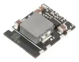


STS1005S1V2
Non Isolated POL DC/DC Converter, ITE, 1 Output, 1.2 W, 1.2 V, 1 A, Fixed, Adjustable
- Manufacturer: XP POWER
- Product type: DC / DC Non Isolated Board Mount Converters - Fixed Output
- Depth: 15.2mm
- Width: 11.8mm
- Height: 3.6mm
- Product Range: STS10 Series
- No. of Outputs: 1 Output
- Output Power Max: 1.2W
- Output Current Max: 1A
- Output Voltage Nom: 1.2V
- Input Voltage DC Max: 5.5V
- Input Voltage DC Min: 3V
- DC / DC Converter Type: Surface Mount DIP
- Power Supply Approvals: ITE
- DC / DC Converter Mounting: Surface Mount Device
- DC / DC Converter Output Type: Fixed, Adjustable
| Delivery and price | |
|---|---|
| Units per pack | 50 |
| Price | 6.19 € |
| Current stock | 10+ |
| Lead time | 30 days |
XP Power

## 1.0 Amp

## • 1A Switching Regulator **xxx Series**

- Regulated Single Outputs from 1.2 to 15VDC

- Wide Input Range

- SMD-10 Package

- Non-Isolated

- Output Voltage Trim ±10%

- High Efficiency up to 96%

- Class B Conducted & Radiated Emissions with External Components

- Short-Circuit Protection

- No Heatsink Required

- Remote On/Off

- Tape & Reel Package Available

Dimensions: STS10: 0.60 x 0.47 x 0.15” (15.20 x 11.80 x 3.6 mm)

- -40°C to +105°C Operation

- Full load to +65°C

- 3 Year Warranty

The STS10 is a new series of innovative low cost DC-DC buck regulators. Based on SMD technology and high levels of automation the series offers many features including voltage trimming, remote on/off, continuous short circuit protection, regulation and high efficiency.

## Models & Ratings

|Nominal Input Voltage<br>(VDC)|Input Voltage<br>(VDC)|Output voltage<br>(VDC)|Output Current<br>(A)<br>~~Ge~~|Output Current<br>Maximum<br>Capacitive Load<br>~~Ge~~|Efficiency at<br>minimum input<br>%<br>~~GO~~|Efficency at<br>maximum<br>input %<br>~~GO~~|Model(1)|
|---|---|---|---|---|---|---|---|
|5 V<br>~~eG~~<br>~~pO~~|3.0-5.5 V<br>~~eG~~<br>|1.2 V<br>~~eG~~<br>|1.0 A<br>~~eG~~<br>~~Ge~~<br>|330μF<br>~~eG~~<br>~~Ge~~<br>|90.5%<br>~~eG~~<br>~~GO~~<br>~~GO~~<br>|90.5%<br>~~eG~~<br>~~GO~~<br>~~GO~~<br>|STS1005S1V2<br>~~eG~~<br>|
|5 V<br>~~GG~~<br>~~pO~~|3.0-5.5 V<br>~~GG~~<br>|1.5 V<br>~~GG~~<br>|1.0 A<br>~~Ge~~<br>~~GG~~<br>|330μF<br>~~Ge~~<br>~~GG~~<br>|92.0%<br>~~GO~~<br>~~GG~~<br>~~GO~~<br>|92.0%<br>~~GO~~<br>~~GG~~<br>~~GO~~<br>|STS1005S1V5<br>~~GG~~<br>|
|5 V<br>~~pO~~|3.0-5.5 V<br>|1.8 V<br>|1.0 A<br>|330μF<br>|92.5%<br>~~GO~~<br><br>~~GO~~|92.5%<br>~~GO~~<br><br>~~GO~~|STS1005S1V8<br>|
|5 V<br>~~pOGG~~|3.8-5.5 V<br>~~GG~~|2.5 V<br>~~GG~~|1.0 A<br>~~GG~~|330μF<br>~~GG~~|94.5%<br>~~GO~~<br>~~GG~~<br>~~GO~~<br>~~GO~~|94.0%<br>~~GO~~<br>~~GG~~<br>~~GO~~<br>~~GO~~|STS1005S2V5<br>~~GG~~|
|24 V<br>~~GG~~<br>~~pO~~|4.6-36.0 V<br>~~GG~~<br>|1.2 V<br>~~GG~~<br>|1.0 A<br>~~GG~~<br>|330μF<br>~~GG~~<br>|87.0%<br>~~GO~~<br>~~GG~~<br>~~GO~~<br>~~DO~~<br>|72.0%<br>~~GO~~<br>~~GG~~<br>~~GO~~<br>~~DO~~<br>|STS1024S1V2<br>~~GG~~<br>|
|24 V<br>~~GG~~<br>~~pO~~|4.6-36.0 V<br>~~GG~~<br>|1.5 V<br>~~GG~~<br>|1.0 A<br>~~GG~~<br>|330μF<br>~~GG~~<br>|89.0%<br>~~GO~~<br>~~GG~~<br>~~DO~~<br>|76.0%<br>~~GO~~<br>~~GG~~<br>~~DO~~<br>|STS1024S1V5<br>~~GG~~<br>|
|24 V<br>~~pO~~|4.6-36.0 V<br>|1.8 V<br>|1.0 A<br>|330μF<br>|90.5%<br>~~DO~~<br><br>~~GO~~|79.0%<br>~~DO~~<br><br>~~GO~~|STS1024S1V8<br>|
|24 V<br>~~pOGG~~|4.6-36.0 V<br>~~GG~~|2.5 V<br>~~GG~~|1.0 A<br>~~GG~~|330μF<br>~~GG~~|92.5%<br>~~DO~~<br>~~GG~~<br>~~GO~~<br>~~GO~~|83.0%<br>~~DO~~<br>~~GG~~<br>~~GO~~<br>~~GO~~|STS1024S2V5<br>~~GG~~|
|24 V<br>~~GG~~|4.75-36.0 V<br>~~GG~~|3.3 V<br>~~GG~~|1.0 A<br>~~GG~~|330μF<br>~~GG~~|94.0%<br>~~GO~~<br>~~GG~~<br>~~GO~~|86.5%<br>~~GO~~<br>~~GG~~<br>~~GO~~|STS1024S3V3<br>~~GG~~|
|24 V<br>~~pT~~|6.5-36.0 V<br>~~pT~~|5.0 V<br>~~pT~~|1.0 A<br>~~pT~~|330μF<br>~~pT~~|95.5%<br>~~GO~~<br>~~pT~~|89.5%<br>~~GO~~<br>~~pT~~|STS1024S05<br>~~pT~~|
|24 V<br>~~ee~~|9.0-36.0 V<br>~~ee~~|6.5 V|1.0 A|330μF|94.5%<br>~~GO~~|90.0%<br>~~GO~~|STS1024S6V5|
|24 V<br>~~GG~~<br>~~pO~~|12.0-36.0 V<br>~~GG~~|9.0 V<br>~~GG~~|1.0 A<br>~~GG~~|330μF<br>~~GG~~|95.5%<br>~~GG~~<br>~~GO~~<br>~~GO~~|92.0%<br>~~GG~~<br>~~GO~~<br>~~GO~~|STS1024S09<br>~~GG~~|
|24 V<br>~~GG~~<br>~~pO~~|15.0-36.0 V<br>~~GG~~|12.0 V<br>~~GG~~|1.0 A<br>~~GG~~|330μF<br>~~GG~~|95.0%<br>~~GO~~<br>~~GG~~<br>~~GO~~|93.0%<br>~~GO~~<br>~~GG~~<br>~~GO~~|STS1024S12<br>~~GG~~|
|24 V<br>~~pO~~|18.0-36.0 V|15.0 V|1.0 A|330μF|96.0%<br>~~GO~~|94.0%<br>~~GO~~|STS1024S15|


~~**Notes**~~

1. For tape & reel add “-TR”, e.g. STS1005S1V5-TR. 500 pcs per reel.

**www.xppower.com**

1

XP Power

## Input

|Characteristic|Minimum|Typical|Maximum|Units|Notes & Conditions|
|---|---|---|---|---|---|
|Input Voltage Range|3|5|5.5|VDC||
||4.6|24|36|||
|Input Surge|||6|VDC for 100 ms|5 V input|
||||40||24 V input|
|Input Current - No Load<br>- Full Load||0.4/1.5||mA|5 V/24 V input|
|||700/900|||5 V/24 V input|
|Input Current - Remote On/Off|||0.3/0.8|mA|5 V/24 V input, idle current|
|Remote On/Off|ON:  Connect pin 10 to voltage of 2-4 V, Logic high<br>OFF: Short pin 10 to pin 9 (0-0.4 V), Logic low|||||


## Output

|Characteristic|Minimum|Typical|Maximum|Units|Notes & Conditions|
|---|---|---|---|---|---|
|Output Voltage|1.2||15|VDC|See Models and Ratings table|
|Initial Set Accuracy|||±2.0|%||
|Minimum Load||||A|No minimum load required|
|Line Regulation|||±0.2|%||
|Load Regulation|||±0.6|%|To 100% load from 10%|
|<4V<br>>4V<br>Transient Response~~——~~|~~=~~|~~=~~|±5|%|Maximum deviation recovery within 250μs at normal Vin for<br>50% step load change from 50% to 100% load|
||~~=~~|~~=~~|±3|||
|Ripple & Noise<br>~~——~~|~~=~~|50<br>~~=~~||mV pk-pk|5 V: 20 MHz bandwidth|
||~~=~~|75<br>~~=~~|||24 V: 20 MHz bandwidth|
|Short Circuit Protection<br>~~——~~|~~=~~|~~=~~|||Continuous, with auto recovery|
|Temperature Coefficient<br>~~——~~|~~=~~|~~=~~|0.02|%/˚C||


## General

|Characteristic|Minimum|Typical|Maximum|Units|Notes & Conditions|
|---|---|---|---|---|---|
|Efficiency|||96|%|See Models and Ratings table|
|Isolation: Input to Output|||||No isolation|
|Switching Frequency||1.2/0.41||MHz|5 V/24 V input|
|Mean Time Between Failure|4.7|||MHrs|MIL-HDBK-217F, +25 °C GB|
|Weight||0.022 (1.4)||lb (g)||
|Moisture Sensitivity Level<br>Level 1|Level 1||||IPC/JEDEC J-STD-020D.1|
|PCB Pad Material<br>Copper|Copper|||||
|PCB Pad Solder Coating<br>Lead-free HASL|Lead-free HASL|||||
|Lead-Free Reflow Solder Process<br>260 °C max, 1.5 mm from case, 10 s max. IPC/JEDEC J-STD-020D.1|260 °C max, 1.5 mm from case, 10 s max. IPC/JEDEC J-STD-020D.1|||||


Environmental Characteristic Minimum Typical Maximum Units Notes & Conditions Operating Temperature -40 +105 °C See Derating Curve. Storage Temperature -55 +125 °C Humidity 95 %RH Non-condensing ~~ee~~ Cooling Natural convection (>30 LFM)

**www.xppower.com**

2

XP Power

## Safety Approvals

|Agency||Standard||Test Level|Notes & Conditions|
|---|---|---|---|---|---|
|CE|Meets all applicable directives|Meets all applicable directives||||
|UKCA|Meets all applicable legislation|Meets all applicable legislation||||


## EMC: Emissions

|Phenomenon|Standard|Test Level|Notes & Conditions|
|---|---|---|---|
|Conducted|EN55032|Class B|With external components, see application note|
|Radiated|EN55032|Class B||


## EMC: Immunity

|Phenomenon|Standard|Test Level|Criteria|Notes & Conditions|
|---|---|---|---|---|
|ESD|EN61000-4-2|±8 kV air discharge|A||
|Radiated|EN61000-4-3|3 V/m|A||
|EFT/Burst|EN61000-4-4|±0.5 kV|A|See application note|
|Surge|EN61000-4-5|±1 kV|A|See application note|
|Conducted|EN61000-4-6|3 V rms|A||
|Magnetic Fields|EN61000-4-8|3 A/m|A||


**==> picture [541 x 309] intentionally omitted <==**

**----- Start of picture text -----**<br>
Mechanical Details<br>EE<br>Top View Bottom View Side View<br>0.1 0.1 0.1 0.1 0.1 0.1 0.1 0.1<br>(2.52)(2.52) (2.52)(2.52) (2.52)(2.52) (2.52)(2.52)<br>0.2 (5.08) 0.2 (5.08) 0.12<br>0.15<br>(2.8)<br>(3.6)<br>1.2 (0.05)<br>i ee 0.6 (15.2)<br>0.47 0.47 0.39<br>STS10<br>(11.8) (11.8) (9.7)<br>1.2 (0.05) 1 .2 (0.05)<br>0.4 (10.16) 0.4 (10.16)<br>0.6 (15.2) 0.6 (15.2)<br>a —<br>Notes<br>Pin Connections<br>Pin Function<br>1 +Vin<br>5 +Vout<br>6 Trim<br>7 -Vout<br>9 -Vin<br>10 Remote On/Off<br>1. All dimensions are in inches (mm)  5. Other Tolerances: ±0.02 (±0.5)<br>2. Weight: 0.0022 lbs (1.4 g) approx.  6. PCB tracks should not run under the STS10 to avoid interference and the risk of<br>short circuit.<br>**----- End of picture text -----**<br>


3. Pin Profile Tolerance: ±0.004 (±0.1)

4. Pin Pitch  Tolerance: ±0.01 (±0.25)

**www.xppower.com**

3

**STS10 Series**

XP Power

**Switching Regulator**

## Application Notes ~~a~~

**Derating Curve STS1005**

**STS1024** Vo= 1.2 V and 1.5 V

**==> picture [476 x 475] intentionally omitted <==**

**----- Start of picture text -----**<br>
100% 100% ttt<br>75% 75%<br>ty A<br>50% 50% ttt<br>tt py<br>25% 25% tet<br>tt ph<br>See<br>-40 -20 0 20 40 60 80 100 105120 -40 -20 0 20 40 60 80 90100 105120<br>STS1024 STS1024<br>Vo= 1.8 V, 2.5 V, 3.3 V and 5 V Vo= 6.5 V and 9 V<br>100% 100%<br>75% tttttttt 75% tttty |<br>50% | AT 50% tttIN |<br>| tt at I |}<br>25% 25%<br>-40 |iEEL -20 0 ttt 20 40 ET 60 EA 80 py 85 100 105120 -40 ittyeee -20 0 tt 20 40  iA 60 er 7080 90100 105120<br>Ambient Temperature (°C) Ambient Temperature (°C)<br>STS1024<br>Vo= 12 V and 15 V<br>Titty<br>100%<br>75%<br>tty |<br>50%<br>ttt TAL<br>25%<br>tet yA [EAT]<br>IN<br>-40 -20 0 20 40 60 65 80 90100 120<br>105<br>Ambient Temperature (°C)<br>EFT & Surge EMI<br>STS STS<br>. Load | = C1 Cin Load<br>ve ; oe | T | + Vin —- +Vout<br>Output Power Output Power<br>Output Power Output Power<br>Output Power<br>**----- End of picture text -----**<br>


## **STS1024**

## **STS1024**

Suggested Filter : 5Vin models : Nippon - chemi - con KY series, 2200 μ F/50 V and a TVS, 3 KW , 6.0 V 24 Vin models : Nippon - chemi - con KY series , 330 μ F/100V and a TVS, 3KW/36V

Input filter components (Cin, C1, L1) are used to help meet EMI requirement for the module. These components should be mounted as close as possible to the module; and all leads should be minimized to decrease radiated noise.

C2 D1 5 V 2200 μ F, 50 V SMDJ 6.0 A 24 V 330 μ F, 100 V SMDF 36.0 A

**==> picture [229 x 27] intentionally omitted <==**

**----- Start of picture text -----**<br>
C1 L1 Cin<br>5 V 1206, 10  μ F, 50 V 6.8  μ H 1206, 10  μ F, 50 V<br>24 V 1206, 4.7  μ F, 50 V 33  μ H 1206, 10  μ F, 50 V<br>**----- End of picture text -----**<br>


**www.xppower.com**

XP Power

## **STS10 Series Switching Regulator** ~~—~~ yyy ee ~~AP.—~~

## **Output Voltage Adjustment**

1 +Vin +Vout 5 Trim-down 100K STS ~~-~~ Vout 7 Pin 6 via a resistor to Pin 5 (+Vout), Vo trim down (Rd) Pin 6 via a resistor to Pin 7(-Vout),Vo trim up (Ru) Trim-up Trim-up /down 9 ~~-~~ Vin TRIM 6

|Model<br>STS1005S1V2<br>STS1005S1V5<br>STS1005S1V8<br>STS1005S2V5<br>~~(S(O~~|
|---|
|V out nominal<br>1V2<br>1V5<br>1V8<br>2V5<br>Trim %<br>Rd*<br>Ru<br>Rd<br>Ru<br>Rd<br>Ru<br>Rd<br>Ru<br>1%<br>-<br>890<br>223<br>955<br>187<br>1000<br>372<br>1600<br>2%<br>-<br>440<br>103<br>475<br>87<br>499<br>172<br>792<br>3%<br>-<br>290<br>63<br>315<br>54<br>332<br>106<br>525<br>4%<br>-<br>215<br>43<br>235<br>37<br>249<br>72<br>393<br>~~a~~<br>~~(~~<br>(<br>(<br>~~(~~<br>~~(S(O~~<br>~~(S(O~~<br>~~( (~~<br>~~eeCO~~<br>~~OO~~<br>~~ee~~<br>~~SO~~<br>~~**O**O~~<br>~~ee~~<br>~~S~~|
|5%<br>-<br>170<br>31<br>187<br>27<br>199<br>52<br>312<br>~~OO~~|
|6%<br>-<br>140<br>23<br>155<br>20<br>166<br>40<br>260<br>~~ee~~|
|7%<br>-<br>118<br>18<br>132<br>15<br>142<br>30<br>221<br>~~Se~~|
|8%<br>-<br>102<br>13<br>115<br>12<br>124<br>22<br>193<br>9%<br>-<br>90<br>10<br>102<br>9<br>110<br>17<br>170<br>10%<br>-<br>80<br>7.3<br>91<br>7<br>100<br>12.5<br>153<br>~~SO~~<br>~~a~~<br>~~CO~~<br>~~(~~<br>~~O~~<br>~~esCC~~<br>~~OO~~|
|Model<br>STS1024S1V2<br>STS1024S1V5<br>STS1024S1V8<br>STS1024S2V5<br>STS1024S3V3<br>STS1024S05<br>STS1024S6V5<br>STS1024S09<br>STS1024S12<br>STS1024S15<br>V out nominal<br>1V2<br>1V5<br>1V8<br>2V5<br>3V3<br>5<br>6V5<br>9<br>12<br>15<br>Trim %<br>Rd*<br>Ru<br>Rd<br>Ru<br>Rd<br>Ru<br>Rd<br>Ru<br>Rd<br>Ru<br>Rd<br>Ru<br>Rd<br>Ru<br>Rd<br>Ru<br>Rd<br>Ru<br>Rd<br>Ru<br>1%<br>-<br>668<br>152<br>1020<br>132<br>876<br>143<br>963<br>226<br>853<br>212<br>941<br>193<br>866<br>230<br>750<br>425<br>1108<br>139<br>714<br>2%<br>-<br>319<br>69<br>514<br>61<br>432<br>71<br>444<br>105<br>424<br>103<br>440<br>94<br>410<br>105<br>380<br>211<br>520<br>67<br>341<br>3%<br>-<br>207<br>41<br>343<br>37<br>286<br>45<br>288<br>65<br>281<br>64<br>285<br>58<br>268<br>64<br>253<br>135<br>337<br>42<br>224<br>4%<br>-<br>152<br>28<br>257<br>25<br>214<br>31<br>213<br>45<br>210<br>44<br>210<br>40<br>198<br>44<br>190<br>96<br>248<br>29<br>166<br>5%<br>-<br>119<br>19<br>206<br>18<br>171<br>23<br>169<br>33<br>167<br>32<br>165<br>30<br>157<br>32<br>151<br>72<br>195<br>21<br>132<br>6%<br>-<br>98<br>14<br>171<br>13<br>142<br>18<br>140<br>25<br>138<br>23<br>136<br>22<br>130<br>24<br>125<br>56<br>160<br>16<br>109<br>7%<br>-<br>82<br>10<br>146<br>10<br>121<br>14<br>119<br>19<br>117<br>17<br>115<br>17<br>110<br>19<br>107<br>45<br>136<br>12<br>93<br>8%<br>-<br>70<br>7<br>128<br>7<br>106<br>10<br>104<br>15<br>103<br>13<br>100<br>13<br>96<br>15<br>93<br>36<br>117<br>10<br>81<br>9%<br>-<br>62<br>5<br>114<br>5<br>94<br>8<br>92<br>11<br>91<br>10<br>88<br>10<br>84<br>11<br>82<br>29<br>103<br>7<br>71<br>10%<br>-<br>54<br>3.2<br>103<br>3.6<br>85<br>6.3<br>83<br>8.5<br>81<br>6.7<br>78<br>7.5<br>75<br>8.6<br>73<br>24<br>92<br>5.6<br>64<br>~~ee Le~~<br>~~CO~~<br>~~(~~<br>~~es~~<br>~~ee~~<br>~~(~~<br>~~CC~~<br>~~CC CY a a CO~~<br>~~Rs~~<br>~~es~~<br>~~esOS~~<br>~~OS~~<br>~~ss~~<br>~~SN~~<br>~~A~~<br>~~OO~~<br>~~I~~<br>~~OC~~<br>~~OO~~<br>~~RsSO~~<br>~~a~~<br>~~Rs ss~~<br>~~SS~~<br>~~OO~~<br>~~OO~~<br>~~OO~~<br>~~NS~~<br>~~sR~~<br>~~OO~~<br>~~OO~~<br>~~CO~~<br>~~CO~~<br>~~sD SO ~~~~**OO** ~~~~**O**S a~~<br>~~Rs ss~~<br>~~OO~~<br>~~S eS~~<br>~~OC~~<br>~~A CO~~<br>~~Rs ~~~~**es**~~<br>~~SS SS~~<br>~~OO ~~~~**OO** SS~~<br>~~es OG~~<br>~~A~~<br>~~CO~~|
|Note: Rd: Trim down. Ru: Trim up. Resistor values in kΩ<br>*1V2 model only trim up|


* 1V2 model only trim up

## **Remote On/Off**

## **Standard Application Circuit**

**==> picture [419 x 47] intentionally omitted <==**

**----- Start of picture text -----**<br>
1 1 5<br>Cin 10  μ F must be fitted near DC-DC pins.<br>10 Optional Cout 47  μ F<br>9 7<br>9 - V in Cin Cou-V tout<br>**----- End of picture text -----**<br>


2-5 VDC or Open DC-DC ON

0-0.4 VDC or Short DC-DC OFF

PCB tracks should not run under the STS10 to avoid interference and the risk of short circuit.

## **Recommended PCB Layout**

Units mm (inches)

26 Nov 2021

**www.xppower.com**

5
Updated at February 9, 2023
XP Power is a globally recognized leader in the design and manufacture of critical power solutions for the electronics industry. With a steadfast commitment to total quality and in-house engineering expertise, the company delivers highly reliable components that support complex applications across the industrial, healthcare, and technology sectors. Their extensive manufacturing capabilities provide engineers with a broad and dependable source for innovative power products. Our extensive portfolio of XP Power components is heavily focused on robust power and line protection. The core of this offering features a vast selection of high-performance AC/DC converters, designed to meet the rigorous efficiency and footprint demands of modern electronic systems. Complementing these are numerous reliable DC/DC converters, providing versatile options for precise voltage regulation and seamless system integration. Beyond their primary power conversion ranges, XP Power manufactures specialized components to address specific design challenges. Our selection includes essential passive components, such as power line filters for effective EMC and RFI suppression, ensuring signal integrity and strict regulatory compliance. Additionally, we provide dedicated AC/DC LED power supplies tailored for reliable, long-lasting performance in advanced commercial and industrial lighting applications.
About Novapart
Novapart is a B2B electronic component broker specialising in stock shortages and cost reduction. We source hard-to-find parts and identify compliant alternatives across a catalogue of 410,000+ components from 500+ manufacturers.
Learn more →Stock Shortage Specialist
When a component is unavailable, discontinued or has an unacceptable lead time, we tap into our network of vetted European and Asian distributors to source what you need — without compromising on quality or traceability.
Request a quote →Compliant Alternatives
We identify pin-to-pin, electrically equivalent substitutes that meet the same certifications (RoHS, AEC-Q100, REACH) as your original specification — validated against datasheets, not just part numbers. Often at a lower cost.
BOM Analysis service →