


STPS41L30CG-TR
Small Signal Schottky Diode, Dual Common Cathode, 30 V, 40 A, 570 mV, 220 A, 150 °C
- Manufacturer: STMICROELECTRONICS
- Product type:
- Diode Configuration:Dual Common Cathode; Repetitive Reverse Voltage Vrrm Max:30V; Forward Current If(AV):40A; Forward Voltage VF Max:570mV; Forward Surge Current Ifsm Max:220A; Operat
- SVHC: No SVHC (25-Jun-2025)
- No. of Pins: 3Pins
- Product Range: STPS4
- Qualification: -
- Diode Mounting: Surface Mount
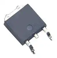
- Diode Case Style: TO-263 (D2PAK)
- Diode Configuration: Dual Common Cathode
- Forward Voltage Max: 570mV
- Forward Surge Current: 220A
- Reverse Recovery Time: -
- Average Forward Current: 40A
- Operating Temperature Max: 150°C
- Repetitive Peak Reverse Voltage: 30V
| Delivery and price | |
|---|---|
| Units per pack | 1000 |
| Price | 0.752 € |
| Current stock | 1000+ |
| Lead time | 30 days |
**==> picture [5 x 6] intentionally omitted <==**

**----- Start of picture text -----**<br>
®<br>**----- End of picture text -----**<br>


## **STPS41L30CG/CT/CR**

## LOW DROP POWER SCHOTTKY RECTIFIER

## **MAIN PRODUCTS CHARACTERISTICS**

**==> picture [220 x 63] intentionally omitted <==**

**----- Start of picture text -----**<br>
IF(AV) 2 x 20 A<br>VRRM 30 V<br>Tj (max) 150 °C<br>VF (max) 0.38 V<br>**----- End of picture text -----**<br>


## **FEATURES AND BENEFITS**

- I VERY SMALL CONDUCTION LOSSES

- I NEGLIGIBLE SWITCHING LOSSES

- I EXTREMELY FAST SWITCHING

- I LOW FORWARD VOLTAGE DROP

- I HIGH AVALANCHE CAPABILITY

- I LOW THERMAL RESISTANCE

- I AVALANCHE CAPABILITY SPECIFIED

## **DESCRIPTION**

Dual center tab Schottky rectifier suited for Switch Mode Power Supply and high frequency DC to DC converters.

Packaged in D[2] PAK, I[2] PAK and TO-220ABthis device is intended for use in low voltage, high frequency inverters, free-wheeling and polarity protection applications.

**==> picture [220 x 289] intentionally omitted <==**

**----- Start of picture text -----**<br>
A1<br>K<br>A2<br>K A2 [A2]<br>A1 [K]<br>A1<br>I [2] PAK TO-220AB<br>STPS41L30CR STPS41L30CT<br>K<br>A2<br>A1<br>D [2] PAK<br>STPS41L30CG<br>**----- End of picture text -----**<br>


## **ABSOLUTE RATINGS** (limiting values, per diode)

**==> picture [461 x 207] intentionally omitted <==**

**----- Start of picture text -----**<br>
Symbol Parameter Value Unit<br>VRRM Repetitive peak reverse voltage 30 V<br>IF(RMS) RMS forward current 30 A<br>IF(AV) Average forward current Tc = 135°C Per diode 20<br>A<br>δ = 0.5 Per device 40<br>IFSM Surge non repetitive forward current tp = 10 ms sinusoidal 220 A<br>IRRM Peak repetitive reverse current tp=2 µs square F=1kHz 1 A<br>PARM Repetitive peak avalanche power tp = 1µs Tj = 25°C 6500 W<br>Tstg Storage temperature range - 65 to + 175 °C<br>Tj Maximum operating junction temperature * 150 °C<br>dV/dt Critical rate of rise reverse voltage 10000 V/µs<br>* : dPtot < 1 thermal runaway condition for a diode on its own heatsink<br>dTj Rth(j − a)<br>**----- End of picture text -----**<br>


July 2003 - Ed : 3A

1/6

## **STPS41L30CG / STPS41L30CT / STPS41L30CR**

## **THERMAL RESISTANCES**

**==> picture [461 x 55] intentionally omitted <==**

**----- Start of picture text -----**<br>
Symbol Parameter Value Unit<br>Rth(j-c) Junction to case Per diode 1.5 °C/W<br>Total 0.8<br>Rth(c) Coupling 0.1<br>**----- End of picture text -----**<br>


When the diodes 1 and 2 are used simultaneously : ∆ Tj(diode 1) = P(diode1) x Rth(j-c)(Per diode) + P(diode 2) x Rth(c)

## **STATIC ELECTRICAL CHARACTERISTICS** (per diode)

**==> picture [461 x 110] intentionally omitted <==**

**----- Start of picture text -----**<br>
Symbol Parameter Tests Conditions Min. Typ. Max. Unit<br>IR * Reverse leakage current Tj = 25°C VR = VRRM 1.5 mA<br>Tj = 125°C 170 350 mA<br>VF * Forward voltage drop Tj = 25°C IF = 20 A 0.48 V<br>Tj = 125°C IF = 20 A 0.35 0.38<br>Tj = 25°C IF = 40 A 0.57<br>Tj = 125°C IF = 40 A 0.47 0.49<br>**----- End of picture text -----**<br>


Pulse test : * tp = 380 µs, δ < 2% To evaluate the conduction losses use the following equation : P = 0.27 x IF(AV) + 0.0055 IF[2] (RMS)

**Fig. 1:** Conduction losses versus average current.

**Fig. 2:** Average forward current versus ambient temperature (δ = 0.5).

**==> picture [461 x 331] intentionally omitted <==**

**----- Start of picture text -----**<br>
PF(av)(W) IF(av)(A)<br>11 25<br>δ = 0.5<br>10<br>δ = 0.2 Rth(j-a)=Rth(j-c)<br>9 δ = 0.1 20<br>8 δ = 1<br>δ = 0.05<br>7<br>15<br>6<br>5<br>10<br>4<br>Rth(j-a)=50°C/W<br>3<br>2 T 5 T<br>1 IF(av)(A) δ [=tp/T] tp δ [=tp/T] tp Tamb(°C)<br>0 0<br>0 5 10 15 20 25 0 25 50 75 100 125 150<br>Fig. 3: Normalized avalanche power derating Fig. 4: Normalized avalanche power derating<br>versus pulse duration. versus junction temperature.<br>PARM(tp) PARM(tp)<br>PARM(1µs) PARM(25°C)<br>1 1.2<br>1<br>0.1 0.8<br>0.6<br>0.01 0.4<br>0.2<br>0.001 tp(µs) 0 T (°C)j<br>0.01 0.1 1 10 100 1000 0 25 50 75 100 125 150<br>**----- End of picture text -----**<br>


2/6

**STPS41L30CG / STPS41L30CT / STPS41L30CR**

**Fig. 5:** Non repetitive surge peak forward current versus overload duration (maximum values).

**==> picture [220 x 142] intentionally omitted <==**

**----- Start of picture text -----**<br>
IM(A)<br>300<br>250<br>200<br>Tc=25°C<br>150<br>Tc=75°C<br>100<br>Tc=125°C<br>50 IM<br>δ=0.5 t t(s)<br>0<br>1.E-03 1.E-02 1.E-01 1.E+00<br>**----- End of picture text -----**<br>


**Fig. 7:** Reverse leakage current versus reverse voltage applied (typical values).

**==> picture [221 x 142] intentionally omitted <==**

**----- Start of picture text -----**<br>
IR(mA)<br>1.E+03<br>Tj=150°C<br>1.E+02 Tj=125°C<br>Tj=100°C<br>1.E+01<br>Tj=75°C<br>1.E+00 Tj=50°C<br>1.E-01 Tj=25°C<br>VR(V)<br>1.E-02<br>0 5 10 15 20 25 30<br>**----- End of picture text -----**<br>


**Fig. 9:** Forward voltage drop versus forward current.

**==> picture [221 x 141] intentionally omitted <==**

**----- Start of picture text -----**<br>
IFM(A)<br>100<br>Tj=125°C<br>(Maximum values)<br>Tj=125°C<br>(Typical values)<br>10<br>Tj=25°C<br>(Maximum values)<br>VFM(V)<br>1<br>0.0 0.1 0.2 0.3 0.4 0.5 0.6 0.7 0.8 0.9 1.0<br>**----- End of picture text -----**<br>


**Fig. 6:** Relative variation of thermal impedance junction to case versus pulse duration.

**==> picture [220 x 143] intentionally omitted <==**

**----- Start of picture text -----**<br>
Zth(j-c)/Rth(j-c)<br>1.0<br>0.9<br>0.8<br>0.7<br>δ = 0.5<br>0.6<br>0.5<br>0.4 δ = 0.2<br>0.3 δ = 0.1<br>T<br>0.2<br>Single pulse<br>0.1 tp(s)<br>δ [=tp/T] tp<br>0.0<br>1.E-03 1.E-02 1.E-01 1.E+00<br>**----- End of picture text -----**<br>


**Fig. 8:** Junction capacitance versus reverse voltage applied (typical values).

**==> picture [220 x 142] intentionally omitted <==**

**----- Start of picture text -----**<br>
C(nF)<br>10.0<br>F=1MHz<br>Vosc=30mV<br>Tj=25°C<br>1.0<br>VR(V)<br>0.1<br>1 10 100<br>**----- End of picture text -----**<br>


**Fig. 10:** Thermal resistance junction to ambient versus copper surface under tab (epoxy printed board FR4, Cu = 35µm) (STPS41L30CG only).

**==> picture [221 x 143] intentionally omitted <==**

**----- Start of picture text -----**<br>
Rth(j-a)(°C/W)<br>80<br>70<br>60<br>50<br>40<br>30<br>20<br>10 S(cm²)<br>0<br>0 5 10 15 20 25 30 35 40<br>**----- End of picture text -----**<br>


3/6

## **STPS41L30CG / STPS41L30CT / STPS41L30CR**

**PACKAGE MECHANICAL DATA** D[2] PAK

**==> picture [461 x 309] intentionally omitted <==**

**----- Start of picture text -----**<br>
DIMENSIONS<br>REF. Millimeters Inches<br>Min. Max. Min. Max.<br>A<br>A 4.40 4.60 0.173 0.181<br>E<br>C 2<br>L2 A1 2.49 2.69 0.098 0.106<br>A2 0.03 0.23 0.001 0.009<br>D B 0.70 0.93 0.027 0.037<br>L<br>B2 1.14 1.70 0.045 0.067<br>L3 C 0.45 0.60 0.017 0.024<br>A1<br>C2 1.23 1.36 0.048 0.054<br>B2 C R D 8.95 9.35 0.352 0.368<br>B<br>E 10.00 10.40 0.393 0.409<br>G<br>G 4.88 5.28 0.192 0.208<br>A2 L 15.00 15.85 0.590 0.624<br>L2 1.27 1.40 0.050 0.055<br>M * L3 1.40 1.75 0.055 0.069<br>V2<br>M 2.40 3.20 0.094 0.126<br>* FLAT ZONE NO LESS THAN 2mm<br>R 0.40 typ. 0.016 typ.<br>V2 0° 8° 0° 8°<br>**----- End of picture text -----**<br>


## **FOOTPRINT** (dimensions in mm)

**==> picture [220 x 80] intentionally omitted <==**

**----- Start of picture text -----**<br>
16.90<br>10.30 5.08<br>1.30<br>3.70<br>8.90<br>**----- End of picture text -----**<br>


4/6

**STPS41L30CG / STPS41L30CT / STPS41L30CR**

**PACKAGE MECHANICAL DATA** I[2] PAK

**==> picture [462 x 304] intentionally omitted <==**

**----- Start of picture text -----**<br>
DIMENSIONS<br>REF. Millimeters Inches<br>Min. Max. Min. Max.<br>A<br>A 4.40 4.60 0.173 0.181<br>E<br>c2 A1 2.49 2.69 0.098 0.106<br>L2<br>b 0.70 0.93 0.028 0.037<br>b1 1.14 1.17 0.044 0.046<br>D b2 1.14 1.17 0.044 0.046<br>c 0.45 0.60 0.018 0.024<br>c2 1.23 1.36 0.048 0.054<br>L1<br>A1 D 8.95 9.35 0.352 0.368<br>b2 e 2.40 2.70 0.094 0.106<br>L<br>b1 E 10.0 10.4 0.394 0.409<br>L 13.1 13.6 0.516 0.535<br>b c L1 3.48 3.78 0.137 0.149<br>e L2 1.27 1.40 0.050 0.055<br>**----- End of picture text -----**<br>


5/6

## **STPS41L30CG / STPS41L30CT / STPS41L30CR**

## **PACKAGE MECHANICAL DATA**

TO-220AB

**==> picture [462 x 304] intentionally omitted <==**

**----- Start of picture text -----**<br>
DIMENSIONS<br>REF. Millimeters Inches<br>Min. Max. Min. Max.<br>H2 A<br>A 4.40 4.60 0.173 0.181<br>Dia C C 1.23 1.32 0.048 0.051<br>L5 D 2.40 2.72 0.094 0.107<br>L7<br>E 0.49 0.70 0.019 0.027<br>F 0.61 0.88 0.024 0.034<br>L6<br>F1 1.14 1.70 0.044 0.066<br>L2<br>F2 1.14 1.70 0.044 0.066<br>F2<br>G 4.95 5.15 0.194 0.202<br>F1 L9 D G1 2.40 2.70 0.094 0.106<br>L4 H2 10 10.40 0.393 0.409<br>F L2 16.4 typ. 0.645 typ.<br>L4 13 14 0.511 0.551<br>M<br>G1 E L5 2.65 2.95 0.104 0.116<br>G L6 15.25 15.75 0.600 0.620<br>L7 6.20 6.60 0.244 0.259<br>L9 3.50 3.93 0.137 0.154<br>M 2.6 typ. 0.102 typ.<br>Diam. 3.75 3.85 0.147 0.151<br>**----- End of picture text -----**<br>


**==> picture [461 x 89] intentionally omitted <==**

**----- Start of picture text -----**<br>
Ordering type Marking Package Weight Base qty Delivery mode<br>STPS41L30CG STPS41L30CG D [2] PAK 1.48 g 50 Tube<br>STPS41L30CG-TR STPS41L30CG D [2] PAK 1.48 g 1000 Tape & reel<br>STPS41L30CT STPS41L30CT TO-220AB 2.20 g 50 Tube<br>STPS41L30CR STPS41L30CR I [2] PAK 1.49 g 50 Tube<br>**----- End of picture text -----**<br>


> I EPOXY MEETS UL94,V0

Information furnished is believed to be accurate and reliable. However, STMicroelectronics assumes no responsibility for the consequences of use of such information nor for any infringement of patents or other rights of third parties which may result from its use. No license is granted by implication or otherwise under any patent or patent rights of STMicroelectronics. Specifications mentioned in this publication are subject to change without notice. This publication supersedes and replaces all information previously supplied. STMicroelectronics products are not authorized for use as critical components in life support devices or systems without express written approval of STMicroelectronics.

The ST logo is a registered trademark of STMicroelectronics

© 2003 STMicroelectronics - Printed in Italy - All rights reserved.

## STMicroelectronics GROUP OF COMPANIES

Australia - Brazil - Canada - China - Finland - France - Germany Hong Kong - India - Israel - Italy - Japan - Malaysia - Malta - Morocco - Singapore Spain - Sweden - Switzerland - United Kingdom - United States.

**http://www.st.com**

6/6
Updated at April 29, 2026
STMicroelectronics is a global leader in the semiconductor industry, recognized for developing highly integrated, energy-efficient solutions that power modern electronics. With a strong focus on innovation, ST provides a comprehensive portfolio of microelectronics that address the demanding requirements of industrial, automotive, communications, and consumer applications. Our extensive selection of STMicroelectronics components is built around a robust lineup of discrete semiconductors and circuit protection devices. We offer a wide variety of single MOSFETs, Schottky diodes, and fast and ultrafast recovery rectifier diodes, designed to deliver exceptional efficiency and thermal performance in power management and conversion systems. For robust circuit protection, our inventory features hundreds of transient voltage suppressors and TVS diodes that safeguard sensitive electronic components against destructive voltage spikes. In addition to core power discretes like TRIACs, SCRs, bipolar transistors, and single IGBTs, our STMicroelectronics range includes specialized integrated passive filters and MEMS sensors. Furthermore, ST offers advanced integrated passive devices, such as baluns and RF filters, which utilize high-quality monolithic RF IPD processes on glass or high-resistance silicon substrates. These components provide competitive cost structures, reduced power losses, and simplified RFIC-to-antenna matching, ensuring optimal system performance and delivering the reliability required for next-generation wireless and power designs.
About Novapart
Novapart is a B2B electronic component broker specialising in stock shortages and cost reduction. We source hard-to-find parts and identify compliant alternatives across a catalogue of 410,000+ components from 500+ manufacturers.
Learn more →Stock Shortage Specialist
When a component is unavailable, discontinued or has an unacceptable lead time, we tap into our network of vetted European and Asian distributors to source what you need — without compromising on quality or traceability.
Request a quote →Compliant Alternatives
We identify pin-to-pin, electrically equivalent substitutes that meet the same certifications (RoHS, AEC-Q100, REACH) as your original specification — validated against datasheets, not just part numbers. Often at a lower cost.
BOM Analysis service →