


STPS30M100DJF-TR
Small Signal Schottky Diode, Single, 100 V, 30 A, 960 mV, 200 A, 150 °C
- Manufacturer: STMICROELECTRONICS
- Product type:
- Diode Configuration:Single; Repetitive Reverse Voltage Vrrm Max:100V; Forward Current If(AV):30A; Forward Voltage VF Max:960mV; Forward Surge Current Ifsm Max:200A; Operating Tempera
- SVHC: No SVHC (25-Jun-2025)
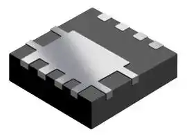
- No. of Pins: 8Pins
- Product Range: STPS3
- Qualification: -
- Diode Mounting: Surface Mount
- Diode Case Style: SMD
- Diode Configuration: Single
- Forward Voltage Max: 960mV
- Forward Surge Current: 200A
- Reverse Recovery Time: -
- Average Forward Current: 30A
- Operating Temperature Max: 150°C
- Repetitive Peak Reverse Voltage: 100V
| Delivery and price | |
|---|---|
| Units per pack | 5000 |
| Price | 0.427 € |
| Current stock | 1000+ |
| Lead time | 30 days |
**STPS30M100DJF**

Datasheet

100 V, 30 A power Schottky rectifier

## **Features**

- Very low conduction losses

- Low forward voltage drop

- Low thermal resistance

- High specified avalanche capability

- High integration

- ECOPACK[®] 2 compliant

## **Applications**

- Switching diode

- SMPS

- DC/DC converter

- LED lighting

- Desktop power supply

## **Description**

The STPS30M100DJF is a power Schottky rectifier optimized for switch mode power supply and high frequency DC to DC converters.

## **Product status link**

STPS30M100DJF

Packaged in PowerFLAT™, this device is intended to be used in adaptors requiring good efficiency at both low and high load. Its low profile was especially designed to be used in applications with space-saving constraints.

PowerFLAT[TM] is a trademark of STMicroelectronics.

|**Product summary**|**Product summary**|
|---|---|
|**Symbol**|**Value**|
|**IF(AV)**|30 A|
|**VRRM**|100 V|
|**Tj (max.)**|150 °C|
|**VF (typ.)**|0.66 V|


**DS6588** - **Rev 6** - **February 2019** For further information contact your local STMicroelectronics sales office.

www.st.com

**STPS30M100DJF Characteristics**

**1**

## **Characteristics**

**Table 1. Absolute Ratings (limiting values at 25 °C, unless otherwise specified, anode terminals short circuited)**

|**Symbol**|**Parameter**|**Parameter**|**Value**|**Unit**|
|---|---|---|---|---|
|VRRM|Repetitive peak reverse voltage||100|V|
|IF(RMS)|Forward rms current||45|A|
|IF(AV)|Average forward current, δ = 0.5, square wave|TC= 90 °C|30|A|
|IFSM|Surge non repetitive forward current|tp= 10 ms sinusoidal|200|A|
|PARM|Repetitive peak avalanche power|tp= 10 µs , Tj= 125 °C|1080|W|
|Tstg|Storage temperature range||-65 to +175|°C|
|Tj|Maximum operating junction temperature(1)||150|°C|


_1. (dPtot/dTj) < (1/Rth(j-a)) condition to avoid thermal runaway for a diode on its own heatsink._

**Table 2. Thermal resistance parameters**

|**Symbol**|**Parameter**|**Max. value**|**Unit**|
|---|---|---|---|
|Rth(j-c)|Junction to case|2.5|°C/W|


For more information, please refer to the following application note :

- AN5046 : Printed circuit board assembly recommendations for STMicroelectronics PowerFLAT™ packages

**Table 3. Static electrical characteristics (anode terminals short circuited)**

|**Symbol**|**Parameter**|**Test conditions**|**Test conditions**|**Min.**|**Typ.**|**Max.**|**Unit**|
|---|---|---|---|---|---|---|---|
|IR (1)|Reverse leakage current|Tj= 25 °C|VR= VRRM|-||100|µA|
|||Tj= 125 °C||-|10|40|mA|
|VF (1)|Forward voltage drop|Tj= 25 °C|IF= 15 A|-||0.82|V|
|||Tj= 125 °C||-|0.58|0.66||
|||Tj= 25 °C|IF= 30 A|||0.96||
|||Tj= 125 °C|||0.66|0.73||


_1. Pulse test: tp = 380 µs, δ < 2%_

To evaluate the conduction losses, use the following equation: P = 0.65 x IF(AV) + 0.00267 x IF[2] (RMS)

For more information, please refer to the following application notes related to the power losses :

- AN604: Calculation of conduction losses in a power rectifier

- AN4021: Calculation of reverse losses on a power diode

**DS6588** - **Rev 6**

**page 2/9**

**STPS30M100DJF Characteristics (curves)**

## **1.1 Characteristics (curves)**

**Figure 1. Average forward power dissipation versus average forward current**

**Figure 2. Average forward current versus ambient temperature (δ = 0.5)**

**==> picture [480 x 370] intentionally omitted <==**

**----- Start of picture text -----**<br>
30.0 PF(AV)(W) 35 IF(AV)(A)<br>| | | | tf tt te tt | {| ft || Rth(j-a) = Rth(j-c) | of ft fT Tf<br>25.0 δ = 0.5 δ = 1 30<br>ptt tt tt ft tt | A 25 | | | | Er N N<br>20.0<br>δ = 0.2<br>P| | | | | 20 a a ee<br>15.0 δ = 0.1<br>δ = 0.05 4 | 15 \<br>10.0 OAL a<br>10<br>77  Ae T a T<br>5.0 5<br>0.0 SPBys Ie IF(AV)(A) δ = t i p / T tp 0 r δ = t iv p o / T tp eeeE e Tamb(°C) IA<br>ee i<br>0 5 10 15 20 25 30 35 0 25 50 75 100 125 150<br>Figure 3. Normalized avalanche power derating versusNormalized avalanche power derating versus Figure 4. Relative variation of thermal impedance junctionRelative variation of thermal impedance junction<br>pulse duration (Tj = 125 °C)j = 125 °C) = 125 °C) to case versus pulse duration<br>PARM(tp)ARM(tp)(tp)tp)p)<br>PARM(10 µs)ARM(10 µs)(10 µs) 1.0 Zth(j-c)/ Rth(j-c)<br>1 — ————--- [ TTT Tt TTT TTTTTT<br>0.9 |a| TTTTa ee |<br>0.8 || | TTTTT PTPAATTTT<br>0.7 aaaa<br>0.1 ———ee 0.6 YT TTPa<br>a<br>0.5 |<br>| TTT PTeT<br>0.4 | || TTTT tTTT CA<br>| TTT Pt<br>0.3 | ce<br>0.01 | | TTTCer<br>0.2 | fermi| TeroT T TTTTTTTP<br>ET TTTTT<br>0.1 Single pulse<br>Fn S o tp(s) it<br>t p(µs)(µs) 0.01.E-05 LT TTT 1.E-04 tTSl 1.E-03 TT 1.E-02 LTOE TT 1.E-01 tT TT} 1.E+00<br>**----- End of picture text -----**<br>


**==> picture [234 x 192] intentionally omitted <==**

**----- Start of picture text -----**<br>
Figure 3. Normalized avalanche power derating versusNormalized avalanche power derating versus<br>pulse duration (Tj = 125 °C)j = 125 °C) = 125 °C)<br>PARM(tp)ARM(tp)(tp)tp)p)<br>PARM(10 µs)ARM(10 µs)(10 µs)<br>1 — ————---<br>0.1 ———ee<br>0.01<br>t p(µs)(µs)<br>0.001<br>1 10 100 1000<br>**----- End of picture text -----**<br>


**Figure 4. Relative variation of thermal impedance junctionRelative variation of thermal impedance junction to case versus pulse duration**

**DS6588** - **Rev 6**

**page 3/9**

**STPS30M100DJF Characteristics (curves)**

**Figure 5. Reverse leakage current versus reverse voltage applied (typical values)**

**Figure 6. Junction capacitance versus reverse voltage applied (typical values)**

**==> picture [226 x 146] intentionally omitted <==**

**----- Start of picture text -----**<br>
1.E+02 IR(mA)<br>Tj = 150 °C<br>1.E+01<br>Tj = 125 °C<br>1.E+00 Tj = 100 °C<br>Tj = 75 °C<br>1.E-01<br>Tj = 50 °C<br>1.E-02 Tj = 25 °C<br>VR(V)<br>1.E-03<br>0 10 20 30 40 50 60 70 80 90 100<br>**----- End of picture text -----**<br>


**==> picture [226 x 145] intentionally omitted <==**

**----- Start of picture text -----**<br>
C(pF)<br>10000<br>F = 1 MHz<br>Vosc = 30 mVRMS<br>T =  25 °C<br>j<br>1000<br>100 VR(V)<br>1 1 0 100<br>**----- End of picture text -----**<br>


**==> picture [513 x 206] intentionally omitted <==**

**----- Start of picture text -----**<br>
Figure 8. Thermal resistance junction to ambient versus<br>Figure 7. Forward voltage drop versus forward current<br>copper surface under tab<br>60 I ( A)F Rth(j-a) (°C/W)<br>150<br>555045 (Maximum values)T =j  125 °C 125 epoxy printed board FR4, eCu = 35 µm PowerFlat™_5X6<br>40<br>100<br>35 T =j  125 °C<br>30 (Typical values)<br>25 75<br>20<br>15 T =j  25 °C 50<br>10 (Maximum values)<br>5 25<br>0 VF (V) SCu(cm²)<br>0.0 0 .1 0.2 0 .3 0.4 0 .5 0.6 0 .7 0.8 0 .9 1.0 1 .1 1.2 0<br>0 1 2 3 4 5 6 7 8 9 10<br>**----- End of picture text -----**<br>


**DS6588** - **Rev 6**

**page 4/9**

**STPS30M100DJF Package information**

**2**

## **Package information**

In order to meet environmental requirements, ST offers these devices in different grades of ECOPACK[®] packages, depending on their level of environmental compliance. ECOPACK[®] specifications, grade definitions and product status are available at: www.st.com. ECOPACK[®] is an ST trademark.

## **2.1 PowerFLAT™ 5x6 package information**

- Epoxy meets UL 94,V0

- Cooling method: by conduction (C)

**Figure 9. PowerFLAT™ 5x6 package outline (non-contractual)**

**==> picture [118 x 139] intentionally omitted <==**

**==> picture [66 x 292] intentionally omitted <==**

**----- Start of picture text -----**<br>
Bottom view<br>Side view<br>Top view<br>**----- End of picture text -----**<br>


**DS6588** - **Rev 6**

**page 5/9**

**STPS30M100DJF PowerFLAT™ 5x6 package information**

**Table 4. PowerFLAT™ 5x6 mechanical data**

||**Dimensions**|**Dimensions**|**Dimensions**|**Dimensions**|**Dimensions**|**Dimensions**|
|---|---|---|---|---|---|---|
|**Rf**|**Millimeters**|||**Inches (for reference only)**|||
|**e**|**Min.**|**Typ.**|**Max.**|**Min.**|**Typ.**|**Max.**|
|A|0.80||1.00|0.031||0.039|
|A1|0.00||0.05|0.000||0.002|
|b|0.30||0.50|0.01||0.02|
|c||0.25|||0.010||
|D|4.80||5.40|0.189||0.212|
|D2|3.91||4.45|0.154||0.175|
|e||1.27|||0.050||
|E|5.90||6.35|0.232||0.250|
|E2|3.34||3.70|0.138||0.146|
|L|0.50||0.80|0.020||0.031|
|K|1.10||1.575|0.015||0.023|
|L1|0.05|0.15|0.25|0.002|0.006|0.009|


**Figure 10. PowerFLAT™ 5x6 recommended footprint (dimensions are in mm)**

**DS6588** - **Rev 6**

**page 6/9**

**STPS30M100DJF Ordering information**

**3 Ordering information**

## **Table 5. Ordering information**

|**Order code**|**Marking**|**Package**|**Weight**|**Base qty.**|**Delivery mode**|
|---|---|---|---|---|---|
|STPS30M100DJF-TR|PS30M 100|PowerFLAT 5x6|0.095 g|3000|Tape and reel|


**DS6588** - **Rev 6**

**page 7/9**

**STPS30M100DJF**

## **Revision history**

**Table 6. Document revision history**

|**Date**|**Version**|**Changes**|
|---|---|---|
|06-Nov-2009|1|First issue.|
|30-Jul-2010|2|Replace Power QFN with PowerFLAT.|
|15-Jan-2011|3|Add reference E in Table 5.|
|20-May-2011|4|Update all package illustrations. Updated base quantity and marking in Table<br>6. Updated terminal identification in captions of Table 2 and Table 4. Added<br>Figure 14.|
|11-Jun-2018|5|Removed figure 5, figure 6 and figure 12.<br>UpdatedTable 1. Absolute Ratings (limiting values at 25 °C, unless otherwise<br>specified, anode terminals short circuited).<br>Minor text changes to improve readability.|
|08-Feb-2019|6|UpdatedSection Cover image,Figure 9. PowerFLAT™ 5x6 package outline<br>(non-contractual)andTable 4. PowerFLAT™ 5x6 mechanical data.|


**DS6588** - **Rev 6**

**page 8/9**

**STPS30M100DJF**

## **IMPORTANT NOTICE – PLEASE READ CAREFULLY**

STMicroelectronics NV and its subsidiaries (“ST”) reserve the right to make changes, corrections, enhancements, modifications, and improvements to ST products and/or to this document at any time without notice. Purchasers should obtain the latest relevant information on ST products before placing orders. ST products are sold pursuant to ST’s terms and conditions of sale in place at the time of order acknowledgement.

Purchasers are solely responsible for the choice, selection, and use of ST products and ST assumes no liability for application assistance or the design of Purchasers’ products.

No license, express or implied, to any intellectual property right is granted by ST herein.

Resale of ST products with provisions different from the information set forth herein shall void any warranty granted by ST for such product.

ST and the ST logo are trademarks of ST. All other product or service names are the property of their respective owners.

Information in this document supersedes and replaces information previously supplied in any prior versions of this document.

© 2019 STMicroelectronics – All rights reserved

**DS6588** - **Rev 6**

**page 9/9**
Updated at April 29, 2026
STMicroelectronics is a global leader in the semiconductor industry, recognized for developing highly integrated, energy-efficient solutions that power modern electronics. With a strong focus on innovation, ST provides a comprehensive portfolio of microelectronics that address the demanding requirements of industrial, automotive, communications, and consumer applications. Our extensive selection of STMicroelectronics components is built around a robust lineup of discrete semiconductors and circuit protection devices. We offer a wide variety of single MOSFETs, Schottky diodes, and fast and ultrafast recovery rectifier diodes, designed to deliver exceptional efficiency and thermal performance in power management and conversion systems. For robust circuit protection, our inventory features hundreds of transient voltage suppressors and TVS diodes that safeguard sensitive electronic components against destructive voltage spikes. In addition to core power discretes like TRIACs, SCRs, bipolar transistors, and single IGBTs, our STMicroelectronics range includes specialized integrated passive filters and MEMS sensors. Furthermore, ST offers advanced integrated passive devices, such as baluns and RF filters, which utilize high-quality monolithic RF IPD processes on glass or high-resistance silicon substrates. These components provide competitive cost structures, reduced power losses, and simplified RFIC-to-antenna matching, ensuring optimal system performance and delivering the reliability required for next-generation wireless and power designs.
About Novapart
Novapart is a B2B electronic component broker specialising in stock shortages and cost reduction. We source hard-to-find parts and identify compliant alternatives across a catalogue of 410,000+ components from 500+ manufacturers.
Learn more →Stock Shortage Specialist
When a component is unavailable, discontinued or has an unacceptable lead time, we tap into our network of vetted European and Asian distributors to source what you need — without compromising on quality or traceability.
Request a quote →Compliant Alternatives
We identify pin-to-pin, electrically equivalent substitutes that meet the same certifications (RoHS, AEC-Q100, REACH) as your original specification — validated against datasheets, not just part numbers. Often at a lower cost.
BOM Analysis service →