


STK541UC62K-E
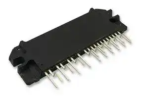
Motor Driver/Controller, Three Phase AC, 13.5V to 16.5V supply, 10 A/1 Output, SIP-23
- Manufacturer: ONSEMI
- Product type: Intelligent Power Modules
- Motor Type:Three Phase AC; No. of Outputs:1Outputs; Output Current:10A; Output Voltage:-; Driver Case Style:SIP; No. of Pins:23Pins; Supply Voltage Min:13.5V; Supply Voltage Max:16.5V; O
- MSL: -
- SVHC: No SVHC (25-Jun-2025)
- Motor Type: Three Phase AC
- No. of Pins: 23Pins
- Product Range: -
- No. of Outputs: 1Outputs
- Output Current: 10A
- Driver Case Style: SIP
- IC Case / Package: SIP
- Supply Voltage Max: 16.5V
- Supply Voltage Min: 13.5V
- Operating Temperature Max: 100°C
- Operating Temperature Min: -40°C
| Delivery and price | |
|---|---|
| Units per pack | 80 |
| Price | 11.06 € |
| Current stock | 10+ |
| Lead time | 30 days |
## **STK541UC62K-E** ## **Intelligent Power Module (IPM) 600 V, 10 A** ## **Overview** This “Inverter IPM” is highly integrated device containing all High Voltage (HV) control from HV-DC to 3-phase outputs in a single SIP module (Single-In line Package). Output stage uses IGBT/FRD technology and implements Under Voltage Protection (UVP) and Over Current Protection (OCP) with a Fault Detection output flag. Internal Boost diodes are provided for high side gate boost drive. www.onsemi.com ## **Function** - Single control power supply due to Internal bootstrap circuit for high side pre-driver circuit - All control input and status output are at low voltage levels directly compatible with microcontrollers - Built-in cross conduction prevention - Externally accessible embedded thermistor for substrate temperature measurement ## **Certification** - UL1557 (File Number : E339285) ## **Specifications** **Absolute Maximum Ratings** at Tc = 25C |Parameter<br>~~es~~<br>~~ee~~|Symbol<br>~~es~~<br>~~es~~|Conditions<br>~~GO~~|Ratings<br>~~GO~~|Unit| |---|---|---|---|---| |Supply voltage<br>~~es~~<br>~~ee~~<br>~~ee~~|VCC<br>~~es~~<br>~~es~~<br>~~es~~|P to N, surge < 500 V<br>*1<br>~~GO~~<br>~~Ge~~|450<br>~~GO~~<br>~~Ge~~|V<br>~~Ge~~| |Collector-emitter voltage<br>~~ee~~<br>~~ee~~|VCE<br>~~es~~<br>~~es~~|P to U, V, W or U, V, W to N<br>~~Ge~~<br>~~__~~|600<br>~~Ge~~|V<br>~~Ge~~| |Output current<br>~~ee~~<br>~~|~~<br>~~ee~~|Io<br>~~es~~<br>~~|~~<br>|P, N, U, V, W terminal current<br>~~Ge~~<br>~~|~~<br>~~__~~|±10<br>~~Ge~~<br>~~|~~|A<br>~~Ge~~<br>~~|~~| |||P, N, U, V, W terminal current at Tc = 100C<br>~~|~~<br>~~__~~<br>~~ee~~<br>|±5<br>~~|~~<br>~~ee~~<br>|A<br>~~|~~<br>~~ee~~<br>| |Output peak current<br>~~ee~~<br>~~ee~~|Iop<br>~~sO~~<br>~~es~~|P, N, U, V, W terminal current for a Pulse width of 1 ms.<br>~~__~~<br>~~ee~~<br>~~sO~~|±20<br>~~ee~~<br>~~sO~~|A<br>~~ee~~<br>~~sO~~| |Pre-driver voltage<br>~~ee~~<br>~~ee~~|VD1, 2, 3, 4<br>~~sO~~<br>~~es~~|VB1 to U, VB2 to V, VB3 to W, VDD to VSS<br>*2<br>~~ee~~<br>~~sO~~|20<br>~~ee~~<br>~~sO~~|V<br>~~ee~~<br>~~sO~~| |Input signal voltage<br><br>~~ee~~<br>~~es~~|VIN<br>~~sO~~<br>~~es~~<br>~~es~~|HIN1, 2, 3, LIN1, 2, 3<br>~~sO~~<br>~~es~~|0.3 to 7<br>~~sO~~<br>~~es~~|V<br>~~sO~~<br>~~es~~| |FLTEN terminal voltage<br>~~es~~<br>~~ee~~|VFLTEN<br>~~es~~<br>~~es~~|FLTEN terminal<br>~~es~~|0.3 to VDD<br>~~es~~|V<br>~~es~~| |Maximum power dissipation<br>~~ee~~<br>~~ee~~|Pd<br>~~es~~<br>~~sO~~|IGBT per channel<br>~~sO~~|22<br>~~sO~~|W<br>~~sO~~| |Junction temperature<br>~~ee~~<br>~~ee~~|Tj<br>~~es~~<br>~~sO~~|IGBT, FRD<br>~~sO~~|150<br>~~sO~~|C<br>~~sO~~| |Storage temperature<br>~~ee~~<br>~~ee es~~|Tstg<br>~~sO~~<br>~~es ee~~|~~sO~~<br>~~ee~~|40 to +125<br>~~sO~~|C<br>~~sO~~| |Operating substrate<br>temperature<br>~~ee es~~<br>~~ee~~|Tc<br>~~es ee~~<br>~~es~~|IPM case temperature<br>~~ee~~|40 to +100|C| |Tightening torque<br>~~ee es~~<br>~~ee~~<br>~~ee~~|~~es ee~~<br>~~es~~<br>~~s~~|Case mounting screws<br>*3<br>~~ee~~|0.9|Nm| |Isolation voltage<br>~~ee~~<br>~~ee~~|Vis<br>~~es~~<br>~~s~~|50 Hz sine wave AC 1 minute<br>*4|2000|VRMS| - *1 : Surge voltage developed by the switching operation due to the wiring inductance between “P” and “N” terminal. - *2 : Terminal voltage: VD1 = VB1 to U, VD2 = VB2 to V, VD3 = VB3 to W, VD4 = VDD to VSS - *3 : Flatness of the heat-sink should be 0.15 mm and below. - *4 : Test conditions : AC 2500 V, 1 s. Stresses exceeding those listed in the Maximum Ratings table may damage the device. If any of these limits are exceeded, device functionality should not be assumed, damage may occur and reliability may be affected. ## **ORDERING INFORMATION** See detailed ordering and shipping information on page 14 of this data sheet. **1** Publication Order Number : **STK541UC62K-E/D** © Semiconductor Components Industries, LLC, 2016 **October 2016 - Rev. 1** ## **STK541UC62K-E** **Electrical Characteristics** at Tc 25C, VD1, VD2, VD3, VD4 = 15 V |**Electrical Characteristics **a|t Tc25C,V|D1,VD2,VD3,VD4 = 15 V|D1,VD2,VD3,VD4 = 15 V|||||| |---|---|---|---|---|---|---|---|---| |Parameter|Symbol|Conditions||Test<br>circuit|min|typ|max|Unit| |**Power output section**||||||||| |Collector-emitter cut-off current|ICE|VCE = 600 V||Fig.1|||0.1|mA| |Bootstrapdiode reverse current|IR(BD)|VR(BD)|||||0.1|mA| |Collector to emitter<br>saturation voltage|VCE(sat)|Ic = 10 A<br>Tj = 25C|Upper side|Fig.2||1.4|2.3|V| ||||Lower side *1|||1.7|2.6|| |||Ic = 5 A<br>Tj = 100C|Upper side|||1.3||| ||||Lower side *1|||1.6||| |Diode forward voltage|VF|IF = 10 A<br>Tj = 25C|Upper side|Fig.3||1.3|2.2|V| ||||Lower side *1|||1.6|2.5|| |||IF = 5 A<br>Tj = 100C|Upper side|||1.2||| ||||Lower side *1|||1.5||| |Junction to case<br>thermal resistance|θj-c(T)|IGBT|||||5.5|C/W| ||θj-c(D)|FRD|||||6.5|| |**Control(Pre-driver) section**||||||||| |Pre-driver current consumption|ID|VD1, 2, 3 = 15 V||Fig.4||0.08|0.4|mA| |||VD4 = 15 V||||1.6|4.0|| |High level Input voltage|Vin H|HIN1, HIN2, HIN3,<br>LIN1, LIN2, LIN3 to VSS|||2.5|||V| |Low level Input voltage|Vin L||||||0.8|V| |Input threshold voltage hysteresis *1|Vinth(hys)||||0.5|0.8||V| |Logic 0 input leakage current|IIN+|VIN = +3.3 V|||76|118|160|A| |Logic 1 input leakage current|IIN-|VIN = 0 V|||97|150|203|A| |FLTEN terminal input electric current|IoSD|FAULT : ON/VFLTEN = 0.1 V||||2||mA| |FAULT clearance delaytime|FLTCLR|Fault output latch time|||6|9|12|ms| |FLTEN Threshold|VEN+|Enable|||2.5|||V| ||VEN-|Disable|||||0.8|| |VCC and VS undervoltage upper<br>threshold|VCCUV+<br>VSUV+||||10.5|11.1|11.7|V| |VCC and VS undervoltage lower<br>threshold|VCCUV-<br>VSUV-||||10.3|10.9|11.5|V| |VCC and VS undervoltage hysteresis|VCCUVH<br>VSUVH-||||0.14|0.2||A| |Over currentprotection level|ISD|PW = 100μs||Fig.5|10||17|A| |Output level for current monitor|ISO|Io = 10 A|||0.30|0.33|0.36|V| Reference voltage is “VSS” terminal voltage unless otherwise specified. *1 : The lower side’s VCE(sat) and VF include a loss by the shunt resistance ## **Electrical Characteristics** at Tc 25C, VD1, VD2, VD3, VD4 = 15 V, VCC = 300 V, L = 3.9 mH |Parameter|Symbol|Conditions|Test<br>circuit|min|typ|max|Unit| |---|---|---|---|---|---|---|---| |**Switching Character**|||||||| |Switching time|tON|Io = 10 A<br>Inductive load|Fig.6|0.2|0.4|1.1|s| ||tOFF||||0.5|1.2|| |Turn-on switchingloss|Eon|Ic = 5 A, P = 300 V,<br>VDD= 15 V, L = 3.9 mH<br>Tc = 25C|Fig.6||200||J| |Turn-off switchingloss|Eoff||||130||J| |Total switchingloss|Etot||||330||J| |Turn-on switchingloss|Eon|Ic = 5 A, P = 300 V,<br>VDD= 15 V, L = 3.9 mH<br>Tc = 100C|Fig.6||240||J| |Turn-off switchingloss|Eoff||||160||J| |Total switchingloss|Etot||||400||J| |Diode reverse recoveryenergy|Erec|IF= 5 A, P = 400 V, VDD= 15 V,<br>L = 0.5 mH, Tc = 100C|||17||J| |Diode reverse recoverytime|Trr||||62||ns| |Reverse bias safe operatingarea|RBSOA|Io = 20 A, VCE= 450 V|||Full square||| |Short circuit safe operatingarea|SCSOA|VCE= 400 V, Tc = 100C||4|||s| |Reference voltage is “VSS” terminal voltage unless otherwise specified.|||||||| Product parametric performance is indicated in the Electrical Characteristics for the listed test conditions, unless otherwise noted. Product performance may not be indicated by the Electrical Characteristics if operated under different conditions. ## Notes : 1. The pre-drive power supply low voltage protection has approximately 0.2 V of hysteresis and operates as follows. - Upper side : The gate is turned off and will return to regular operation when recovering to the normal voltage, but the latch will continue till the input signal will turn ‘high’. Lower side : The gate is turned off and will automatically reset when recovering to normal voltage. It does not depend on input signal voltage. 2. The pre-drive low voltage protection is the feature to protect devices when the pre-driver supply voltage falls due to an operating malfunction. **www.onsemi.com** **2** **STK541UC62K-E** ## **Equivalent Block Diagram** **==> picture [465 x 490] intentionally omitted <==** **----- Start of picture text -----**<br> VB1(7)<br>U(8)<br>VB2(4)<br>V(5)<br>VB3(1)<br>W(2)<br>P(10)<br>U.V. U.V. U.V.<br>Shunt Resistor<br>N(12)<br>Level Level Level<br>Thermistor Shifter Shifter Shifter<br>VTH (13)<br>HIN1(15)<br>HIN2(16)<br>HIN3(17) Logic Logic Logic<br>LIN1(18)<br>LIN2(19)<br>LIN3(20)<br>FLTEN(21)<br>ISO(22) Latch Time About 9ms<br>Latch ( Automatic Reset )<br>VDD(14)<br>Over-Current<br>VSS(23)<br>VDD-Under Voltage<br>**----- End of picture text -----**<br> **www.onsemi.com** **3** **STK541UC62K-E** ## **Module Pin-Out Description** |**Pin**|**Name**|**Description**| |---|---|---| |1|VB3|High Side Floating Supply Voltage 3| |2|W, VS3|Output 3 - High Side Floating Supply Offset Voltage| |3||Witout Pin| |4|VB2|High Side Floating Supply voltage 2| |5|V,VS2|Output 2 - High Side Floating Supply Offset Voltage| |6||Witout Pin| |7|VB1|High Side Floating Supply voltage 1| |8|U,VS1|Output 1 - High Side Floating Supply Offset Voltage| |9||Witout Pin| |10|P|Positive Bus Input Voltage| |11||Witout Pin| |12|N|Negative Bus Input Voltage| |13|VTH|Temperature Feedback| |14|VDD|+15 V Main Supply| |15|HIN1|Logic Input High Side Gate Driver - Phase U| |16|HIN2|Logic Input High Side Gate Driver - Phase V| |17|HIN3|Logic Input High Side Gate Driver - Phase W| |18|LIN1|Logic Input Low Side Gate Driver - Phase U| |19|LIN2|Logic Input Low Side Gate Driver - Phase V| |20|LIN3|Logic Input Low Side Gate Driver - Phase W| |21|FLTEN|Fault output and Enable| |22|ISO|Current monitor output| |23|VSS|Negative Main Supply| **www.onsemi.com** **4** **STK541UC62K-E** ## **Test Circuit** The tested phase U+ shows the upper side of the U phase and U shows the lower side of the U phase. ## ■ ICE / IR(BD) ||U+|V+|W+|U-|V-|W-| |---|---|---|---|---|---|---| |M|10|10|10|8|5|2| |N|8|5|2|12|12|12| ||U(BD)|V(BD)|W(BD)| |---|---|---|---| |M|7|4|1| |N|23|23|23| **==> picture [202 x 130] intentionally omitted <==** **----- Start of picture text -----**<br> ICE<br>1 M A<br>VD3=15V<br>2<br>4<br>VD2=15V<br>5 VCE<br>7<br>VD1=15V<br>8<br>14<br>VD4=15V<br>23 N<br>**----- End of picture text -----**<br> Fig.1 ## ■ VCE(sat) (test by pulse) ||U+|V+|W+|U-|V-|W-| |---|---|---|---|---|---|---| |M|10|10|10|8|5|2| |N|8|5|2|12|12|12| |m|15|16|17|18|19|20| **==> picture [199 x 138] intentionally omitted <==** **----- Start of picture text -----**<br> 1 M<br>VD3=15V<br>2<br>4<br>VD2=15V<br>5<br>V Ic<br>7<br>VD1=15V VCE(SAT)<br>8<br>14<br>VD4=15V<br>m N<br>23<br>**----- End of picture text -----**<br> Fig.2 ## ■ VF (test by pulse) ||U+|V+|W+|U-|V-|W-| |---|---|---|---|---|---|---| |M|10|10|10|8|5|2| |N|8|5|2|12|12|12| **==> picture [129 x 86] intentionally omitted <==** **----- Start of picture text -----**<br> M<br>V VF IF<br>N<br>**----- End of picture text -----**<br> Fig.3 ## ■ ID ||VD1|VD2|VD3|VD4| |---|---|---|---|---| |M|7|4|1|14| |N|8|5|2|23| **==> picture [144 x 62] intentionally omitted <==** **----- Start of picture text -----**<br> ID<br>A M<br>VD*<br>N<br>**----- End of picture text -----**<br> Fig.4 **www.onsemi.com** **5** **STK541UC62K-E** ## ■ ISD **==> picture [408 x 147] intentionally omitted <==** **----- Start of picture text -----**<br> 1 8<br>VD3=15V<br>2<br>4<br>VD2=15V<br>Input signal 5<br>(0 to 5 V) Io<br>7<br>VD1=15V<br>8<br>Io SD 14<br>VD4=15V<br>100μS Input signal 18 23 12<br>**----- End of picture text -----**<br> Fig.5 ■ Switching time (The circuit is a representative example of the lower side U phase.) **==> picture [164 x 120] intentionally omitted <==** **----- Start of picture text -----**<br> Input signal<br>(0 to 5 V)<br>90%<br>Io<br>10%<br>tOFF<br>**----- End of picture text -----**<br> **==> picture [227 x 155] intentionally omitted <==** **----- Start of picture text -----**<br> 1 10<br>VD1=15V<br>2<br>4<br>VD2=15V<br>5 8 Vcc<br>7 CS<br>VD3=15V<br>8<br>14<br>VD4=15V Io<br>Input signal 18 12<br>23<br>**----- End of picture text -----**<br> Fig.6 **www.onsemi.com** **6** **STK541UC62K-E** ## **Input / Output Timing Diagram** **==> picture [489 x 573] intentionally omitted <==** **----- Start of picture text -----**<br> VBS undervoltage protection reset signal<br>OFF<br>HIN1,2,3<br>ON<br>LIN1,2,3<br>VDD undervoltage protection reset voltage<br>*2<br>VDD<br>VBS undervoltage protection reset voltage<br>*3<br>VB1,2,3<br>*4<br>-------------------------------------------------------ISD operation current level-------------------------------------------------------<br>-terminal<br>(BUS line)<br>Current<br>FLTEN terminal<br>Voltage<br>(at pulled-up)<br>ON<br>*1<br>Upper<br>U, V, W<br>OFF<br>*1<br>Lower<br>U ,V, W<br>Automatically reset after protection<br>(typ.9ms)<br>Fig.7<br>**----- End of picture text -----**<br> ## Notes - *1 : Diagram shows the prevention of shoot-through via control logic. More dead time to account for switching delay needs to be added externally. - *2 : When VDD decreases all gate output signals will go low and cut off all of 6 IGBT outputs. When VDD rises the operation will resume immediately. - *3 : When the upper side gate voltage at VB1, VB2 and VB3 drops only, the corresponding upper side output is turned off. The outputs return to normal operation immediately after the upper side gate voltage rises. - *4 : In case of over current detection, all IGBT’s are turned off and the FAULT output is asserted. Normal operation resumes in 6 to 12ms after the over current condition is removed. **www.onsemi.com** **7** **STK541UC62K-E** ## **Logic level table** |HIN1,2,3<br>(15,16,17)<br>LIN1,2,3<br>(18,19,20)|Ho<br> <br>IC<br>Driver<br>Lo<br> <br>P<br>N|U,V,W<br>(8,5,2)|||INPUT||||OUTPUT|| |---|---|---|---|---|---|---|---|---|---|---| ||||HIN|LIN|OCP|FAULTEN|Upper<br>IGBT|Lower<br>IGBT|U,V,W|FAULTEN| ||||H|L|OFF|Pulled-UP|OFF|ON|N|OFF| ||||L|H|OFF|Pulled-UP|ON|OFF|P|OFF| ||||L|L|OFF|Pulled-UP|OFF|OFF|High<br>Impedance|OFF| ||||H|H|OFF|Pulled-UP|OFF|OFF|High<br>Impedance|OFF| ||||X|X|ON|Pulled-UP|OFF|OFF|High<br>Impedance|ON| ||||X|X|OFF|L|OFF|OFF|High<br>Impedance|ON| |||||||||||| Fig. 8 **www.onsemi.com** **8** **STK541UC62K-E** ## **Sample Application Circuit** **==> picture [379 x 181] intentionally omitted <==** **----- Start of picture text -----**<br> STK541UC62K-E<br>1 2 4 5 7 8 10 12 15 16 17 18 19 20 21 22 14 23 13<br>CB CB CB<br>CS<br>RP<br>VP<br>CD<br>Control Logic VDD=15V<br>Vcc CI<br>VB3 W VB2 V VB1 U P N HIN1 HIN2 HIN3 LIN1 LIN2 LIN3 FLTEN ISO VDD VSS VTH<br>**----- End of picture text -----**<br> Fig. 9 ## **Recommended Operating Conditions** |Item|Symbol|Conditions|Conditions|min|typ|max|Unit| |---|---|---|---|---|---|---|---| |Supplyvoltage|VCC|P to N||0|280|450|V| |Pre-driver supply voltage|VD1, 2, 3|VB1 to U, VB2 to V, VB3 to W||12.5|15|17.5|V| ||VD4|VDD to VSS|*1|13.5|15|16.5|| |ON-state input voltage|VIN(ON)|HIN1, HIN2, HIN3,<br>LIN1, LIN2, LIN3||0||0.3|V| |OFF-state input voltage|VIN(OFF)|||3.0||5.0|| |PWM frequency|fPWM|||1||20|kHz| |Dead time|DT|Turn-off to turn-on||2|||μs| |Allowable inputpulse width|PWIN|ON and OFF||1|||μs| |Tighteningtorque||‘M3’ type screw||0.6||0.9|Nm| *1 Pre-drive power supply (VD4 = 15 ±1.5 V) must have the capacity of Io = 20 mA (DC), 0.5 A (Peak). Functional operation above the stresses listed in the Recommended Operating Ranges is not implied. Extended exposure to stresses beyond the Recommended Operating Ranges limits may affect device reliability. ## **Usage Precaution** 1. This IPM includes bootstrap diode and resistors. Therefore, by adding a capacitor “CB”, a high side drive voltage is generated; each phase requires an individual bootstrap capacitor. The recommended value of CB is in the range of 1 to 47 μF, however this value needs to be verified prior to production. If selecting the capacitance more than 47 μF (±20%), connect a resistor (about 20 Ω) in series between each 3-phase upper side power supply terminals (VB1,2,3) and each bootstrap capacitor. When not using the bootstrap circuit, each upper side pre-drive power supply requires an external independent power supply. 2. It is essential that wirning length between terminals in the snubber circuit be kept as short as possible to reduce the effect of surge voltages. Recommended value of “CS” is in the range of 0.1 to 10 μF. 3. “ISO” (pin22) is terminal for current monitor. When the pull-down resistor is used, please select it more than 5.6 kΩ 4. “FLTEN” (pin21) is open DRAIN output terminal (Active Low). Pull up resistor is recommended more than 5.6 kΩ. 5. Inside the IPM, a thermistor used as the temperature monitor for internal subatrate is connected between VSS terminal and VTH terminal, therefore, an external pull up resistor connected between the TH terminal and an external power supply should be used. The temperature monitor example application is as follows, please refer the Fig.10 and below. 6. The over-current protection feature is not intended to protect in exceptional fault condition. An external fuse is recommended for safety. 7. When “N” and “VSS” terminal are short-circuited on the outside, level that over-current protection (ISD) might be changed from designed value as IPM. Please check it in your set (“N” terminal and “VSS” terminal are connected in IPM). 8. When input pulse width is less than 1.0 μs, an output may not react to the pulse. (Both ON signal and OFF signal) This data shows the example of the application circuit, does not guarantee a design as the mass production set. **www.onsemi.com** **9** **STK541UC62K-E** ## **The characteristic of thermistor** |Parameter|Symbol|Condition|Min|Typ.|Max|Unit| |---|---|---|---|---|---|---| |Resistance|R25|Tc = 25C|99|100|101|kΩ| |Resistance|R100|Tc = 100C|5.12|5.38|5.66|kΩ| |B-Constant (25 to 50C)|B||4165|4250|4335|K| |Temperature Range|||40||+125|C| ## Case Temperature(Tc) - Thermal resistance(RTH) **==> picture [418 x 248] intentionally omitted <==** **----- Start of picture text -----**<br> 10000<br>min<br>typ<br>1000<br>max<br>100<br>10<br>1<br>-40 -30 -20 -10 0 10 20 30 40 50 60 70 80 90 100 110 120 130<br>Case temperature, Tc-degC<br>Thermistor Resistanse, RTH-Kohm<br>**----- End of picture text -----**<br> Fig.10 Variation of thermistor resistance with temperature ## Case Temperature(Tc) - TH terminal voltage(VTH) **==> picture [418 x 249] intentionally omitted <==** **----- Start of picture text -----**<br> 6.0<br>min<br>5.0 typ<br>max<br>4.0<br>3.0<br>2.0<br>1.0<br>0.0<br>-40 -30 -20 -10 0 10 20 30 40 50 60 70 80 90 100 110 120 130<br>Case temperature, Tc-degC<br>-V<br>TH<br>Thermistor Pin Read-Out Voltage, V<br>**----- End of picture text -----**<br> Fig.11 Variation of thermistor terminal voltage with temperature (47 k pull-up resistor, 5 V) **www.onsemi.com** **10** **STK541UC62K-E** ## **The characteristic of PWM switching frequency** **==> picture [390 x 243] intentionally omitted <==** **----- Start of picture text -----**<br> 14<br>12<br>10<br>8<br>6<br>4<br>2<br>0<br>0 2 4 6 8 10 12 14 16 18 20<br>PWM Switching Frequency (kHz)<br>(A)<br>Maximum RMS Output Current / Phase<br>**----- End of picture text -----**<br> Fig. 12 Maximum sinusoidal phase current as function of switching frequency at Tc = 100℃, VCC = 400 V **www.onsemi.com** **11** **STK541UC62K-E** ## **CB capacitor value calculation for bootstrap circuit** ## **Calculate conditions** |**alculate conditions**|||| |---|---|---|---| |Parameter|Symbol|Value|Unit| |Upper side power supply|VBS|15|V| |Total gate charge of output power IGBT at 15 V|QG|89|nC| |Upper limit power supply low voltage protection|UVLO|12|V| |Upper side power dissipation|IDMAX|400|μA| |ON time required for CB voltage to fall from 15 V to UVLO|TONMAX||s| ## **Capacitance calculation formula** Thus, the following formula are true VBS x CB - QG - IDMAX * TONMAX = UVLO * CB therefore, CB = (QG + IDMAX * TONMAX) / (VBS - UVLO) The relationship between TONMAX and CB becomes as follows. CB is recommended to be approximately 3 times the value calculated above. The recommended value of CB is in the range of 1 to 47 μF, however, this value needs to be verified prior to production. **==> picture [393 x 250] intentionally omitted <==** **----- Start of picture text -----**<br> CB vs Tonmax<br>100<br>10<br>1<br>0.1<br>0.01<br>0.1 1 10 100 1000<br>Tonmax [ms]<br>Bootstrap Capacitance CB [uF]<br>**----- End of picture text -----**<br> Fig. 15 Tonmax - CB characteristic **www.onsemi.com** **12** **STK541UC62K-E** ## **PACKAGE DIMENSIONS** unit : mm The tolerances of length are +/ 0.5 mm unless otherwise specified. **==> picture [206 x 178] intentionally omitted <==** **----- Start of picture text -----**<br> 56.0<br>note2 note3<br>4DB00<br>STK541UC62K<br>note1 1 23<br>2.0 0.6 [+0.2] -0.05<br>22.0 2.0<br>22 x 2.0 = 44.0<br>R1.7<br>**----- End of picture text -----**<br> **==> picture [185 x 116] intentionally omitted <==** **----- Start of picture text -----**<br> 46.2<br>50.0<br>62.0<br>5.0<br>2.0<br>**----- End of picture text -----**<br> missing pin ; 3, 6, 9, 11 **==> picture [126 x 135] intentionally omitted <==** **----- Start of picture text -----**<br> 0.5 [+0.2] -0.05<br>5.0<br>3.2<br>3.4<br>21.8<br>(10.9)<br>9.0<br>0.5<br>4.3<br>**----- End of picture text -----**<br> note1 : Mark for No.1 pin identification. note2 : The form of a character in this drawing differs from that of IPM. note3 : This indicates the date code. The form of a character in this drawing differs from that of IPM. **www.onsemi.com** **13** **STK541UC62K-E** ## **ORDERING INFORMATION** |**ORDERING INFORMATION**||| |---|---|---| |Device|Package|Shipping (Qty / Packing)| |STK541UC62K-E|SIP23 56x21.8<br>(Pb-Free)|8 / Tube| ON Semiconductor and the ON Semiconductor logo are trademarks of Semiconductor Components Industries, LLC dba ON Semiconductor or its subsidiaries in the United States and/or other countries. ON Semiconductor owns the rights to a number of patents, trademarks, copyrights, trade secrets, and other intellectual property. A listing of ON Semiconductor’s product/patent coverage may be accessed at www.onsemi.com/site/pdf/Patent-Marking.pdf. ON Semiconductor reserves the right to make changes without further notice to any products herein. ON Semiconductor makes no warranty, representation or guarantee regarding the suitability of its products for any particular purpose, nor does ON Semiconductor assume any liability arising out of the application or use of any product or circuit, and specifically disclaims any and all liability, including without limitation special, consequential or incidental damages. Buyer is responsible for its products and applications using ON Semiconductor products, including compliance with all laws, regulations and safety requirements or standards, regardless of any support or applications information provided by ON Semiconductor. “Typical” parameters which may be provided in ON Semiconductor data sheets and/or specifications can and do vary in different applications and actual performance may vary over time. All operating parameters, including “Typicals” must be validated for each customer application by customer’s technical experts. ON Semiconductor does not convey any license under its patent rights nor the rights of others. ON Semiconductor products are not designed, intended, or authorized for use as a critical component in life support systems or any FDA Class 3 medical devices or medical devices with a same or similar classification in a foreign jurisdiction or any devices intended for implantation in the human body. Should Buyer purchase or use ON Semiconductor products for any such unintended or unauthorized application, Buyer shall indemnify and hold ON Semiconductor and its officers, employees, subsidiaries, affiliates, and distributors harmless against all claims, costs, damages, and expenses, and reasonable attorney fees arising out of, directly or indirectly, any claim of personal injury or death associated with such unintended or unauthorized use, even if such claim alleges that ON Semiconductor was negligent regarding the design or manufacture of the part. ON Semiconductor is an Equal Opportunity/Affirmative Action Employer. This literature is subject to all applicable copyright laws and is not for resale in any manner. **www.onsemi.com** **14**
Updated at April 27, 2026
onsemi is a premier global supplier of intelligent power and sensing technologies, driving disruptive innovations across the automotive, industrial, and cloud infrastructure markets. Recognized for their commitment to sustainability and reliable supply chains, the company accelerates advancements in vehicle electrification, industrial automation, and 5G networks by solving the industry's most complex design challenges. At the core of their portfolio is an industry-leading selection of discrete semiconductors. This extensive range features thousands of high-performance bipolar transistors, single and dual MOSFETs, and a comprehensive array of diodes, including Zener, Schottky, and fast-recovery rectifiers. Engineered for superior thermal performance and energy efficiency, these foundational components are critical for demanding power conversion, switching, and signal conditioning applications. Beyond essential discretes, onsemi provides a robust suite of advanced power management and circuit protection solutions. Their lineup includes intelligent power modules, single IGBTs, and transient voltage suppression (TVS) diodes designed to safeguard sensitive circuitry. Complimented by integrated passive filters, AC/DC LED driver ICs, and specialized sub-2.4GHz RF transceivers, onsemi equips engineers with the scalable, high-quality technologies needed to build a cleaner, smarter, and more connected world.
About Novapart
Novapart is a B2B electronic component broker specialising in stock shortages and cost reduction. We source hard-to-find parts and identify compliant alternatives across a catalogue of 410,000+ components from 500+ manufacturers.
Learn more →Stock Shortage Specialist
When a component is unavailable, discontinued or has an unacceptable lead time, we tap into our network of vetted European and Asian distributors to source what you need — without compromising on quality or traceability.
Request a quote →Compliant Alternatives
We identify pin-to-pin, electrically equivalent substitutes that meet the same certifications (RoHS, AEC-Q100, REACH) as your original specification — validated against datasheets, not just part numbers. Often at a lower cost.
BOM Analysis service →