


STF202-22T1G
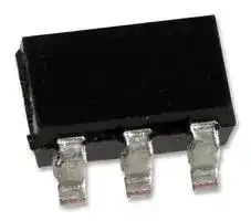
EMI Filter, 3-Channel, USB Line Termination, ESD Protection, TSOP-6
- Manufacturer: ONSEMI
- Product type: Integrated Passive Filters
- EMI Filter Type:EMI Filter with ESD Protection; No. of Data Lines:3 Data Lines; Filter Circuit:RC Pi Filter; Filter Case Style:TSOP; No. of Pins:6Pins; Product Range:STF20 Series; SVHC:No SVHC
- SVHC: No SVHC (27-Jun-2024)
- No. of Pins: 6Pins
- Product Range: -
- Filter Circuit: RC Pi Filter
- EMI Filter Type: EMI Filter with ESD Protection
- No. of Data Lines: 2 Data Lines
- Filter Case / Package: TSOP
| Delivery and price | |
|---|---|
| Units per pack | 3000 |
| Price | 0.217 € |
| Current stock | 10+ |
| Lead time | 30 days |
STF202-22T1G

## USB Filter with ESD Protection

This device is designed for applications requiring **Line Termination** , **EMI Filtering** and **ESD Protection** . It is intended for use in upstream USB ports, Cellular phones, Wireless equipment and computer applications. This device offers an integrated solution in a small package (TSOP−6, Case 318G) reducing PCB space and cost.

## **http://onsemi.com**

## **CIRCUIT DESCRIPTION**

## **Features:**

- Provides USB Line Termination, Filtering and ESD Protection

**==> picture [469 x 231] intentionally omitted <==**

**----- Start of picture text -----**<br>
GND D(OUT) D(OUT)<br>• Single IC Offers Cost Savings by Replacing 3 Resistors, 6 5 4<br>2 Capacitors, and 5 TVs diodes<br>• Bi−directional EMI Filtering Prevents Noise from Entering/Leaving<br>the System<br>• IEC61000−4−2 ESD Protection for USB Port C Rs1 C Rs2<br>• Flexible Pull−down or Pull−up Line Termination to Meet USB 1.1<br>Low Speed and High Speed Specification<br>• ESD Ratings: Machine Model = C Rup<br>ESD Ratings: Human Body Model = 3B 1 2 3<br>• This is a Pb−Free Device VBUS D(IN) D(IN)<br>Benefits:<br>• TSOP−6 Package Minimizes PCB Space 4<br>5<br>• Integrated Circuit Increases System Reliability versus Discrete 6<br>me<br>Component Implementation [3]<br>1 [2]<br>• TVs Devices Provide ESD Protection That is Better than a Discrete<br>TSOP−6<br>Implementation because the Small IC minimizes Parasitic<br>CASE 318G<br>Inductances<br>STYLE 8<br>**----- End of picture text -----**<br>


## **Typical Applications:**

**MARKING DIAGRAM**

- USB Hubs

6 5 4 • Computer Peripherals Using USB **MAXIMUM RATINGS** (TA = 25 ° C) S22 M **Rating Symbol Value Unit** Steady State Power PD 225 mW 1 2 3 Maximum Junction Temperature TJ(max) 125 ° C S22 = Specific Device Code M = Date Code Operating Temperature Range TJ −55 to +125 ° C = Pb−Free Package Storage Temperature Range Tstg −55 to +125 ° C (Note: Microdot may be in either location) Lead Solder Temperature TL 260 ° C ~~=e~~ (10 second duration) **ORDERING INFORMATION** Stresses exceeding Maximum Ratings may damage the device. Maximum Ratings are stress ratings only. Functional operation above the Recommended **Device Package Shipping**[[†]] Operating Conditions is not implied. Extended exposure to stresses above the STF202−22T1G TSOP−6 3000/Tape & Reel Recommended Operating Conditions may affect device reliability.

**Device Package Shipping**[[†]] STF202−22T1G TSOP−6 3000/Tape & Reel (Pb−Free) ~~pr~~ †For information on tape and reel specifications, including part orientation and tape sizes, please refer to our Tape and Reel Packaging Specification Brochure, BRD8011/D.

Publication Order Number: **STF202−22T1/D**

**1**

© Semiconductor Components Industries, LLC, 2012 **September, 2012 − Rev. 9**

**STF202−22T1G**

## **ELECTRICAL CHARACTERISTICS** (TA = 25 ° C)

|**ELECTRICAL C**|**HARACTE**|**RISTIC**|**S**(TA= 25°C|**S**(TA= 25°C|)|||||||||
|---|---|---|---|---|---|---|---|---|---|---|---|---|---|
|**Device**|**Device**<br>**Marking**|**VRWM**<br>**(Volts)**|**VBR@**<br>**1 mA**<br>**(Volts)**||**Max IR**<br>**@ VRWM**<br>**= 5.25 V**<br>**VBUS to**<br>**GND**<br>**(�A)**<br>|**Max IR**<br>**@ VRWM**<br>**= 3.3 V**<br>**I/O Pin**<br>**(�A)**|**Typical Line**<br>**Capacitance**<br>**(pF)**<br>(Notes 2, 3)|**Series Resistor**<br>**RS (�) **(Note 1)|||**Pull−up Resistor**<br>**Rup (k�)**|||
||||**Min**|**Max**||||**Min**|**Nom**|**Max**|**Min**|**Nom**|**Max**|
|STF202−22T1G|S22|5.25|6.0|8.0|5.0|1.0|68|20|22|24|1.35|1.5|1.65|


1. For other RS values (i.e. RS = 30 � ) contact your local ON Semiconductor sales representative.

2. Measured at 25 ° C, VR = 0 V, f = 1 MHz, Pins 2, 3, 4 or 5 to GND with Pin 1 also grounded.

3. For other capacitance values contact your local ON Semiconductor sales representative.

## **TYPICAL CHARACTERISTICS**

**==> picture [489 x 390] intentionally omitted <==**

**----- Start of picture text -----**<br>
10 50<br>0 40<br>−10 P = −25 dBm 30 P = −25 dBm<br>Vdc = 0 V Vdc = 0 V<br>−20 20<br>−30 10<br>−40 0<br>−50 −10<br>−60 −20<br>−70 −30<br>−80 −40<br>−90 −50<br>0.1 1 10 100 1000 0.1 1 10 100 1000<br>(MHz) (MHz)<br>Figure 1. Analog Cross−talk (D+ to D−) Figure 2. Insertion Loss Characteristics<br>22.2 1540<br>RS− TARGET 1530<br>22.0 TARGET<br>1520<br>21.8 1510<br>1500<br>21.6<br>1490<br>21.4 1480<br>1470<br>21.2<br>1460<br>21.0 1450<br>−30 −20 −10 0 10 20 30 40 50 60 70 80 −30 −20 −10 0 10 20 30 40 50 60 70 80<br>TEMPERATURE ( ° C) TEMPERATURE ( ° C)<br>(dB) (dB)<br>(Ohms)  (Ohms)<br>S  up<br>R R<br>**----- End of picture text -----**<br>


**Figure 3. RS versus Temperature**

**Figure 4. Rup versus Temperature**

**http://onsemi.com**

**2**

**STF202−22T1G**

## **APPLICATIONS BACKGROUND**

## **What Is USB?**

The USB is not a serial port, it is a serial bus, a fact that enables a single port on the computer to be a link for a myriad of devices, (up to 127 devices in a USB system). We can easily chain one device to another and use one port as a connecting point of many devices by using a hub. All these enables us to look at the USB system as a small network of devices.

The Universal Serial Bus (USB) makes connecting devices to your computer faster, easier and virtually limitless. High−Speed USB devices are capable of communicating at speeds up to 12 megabits without shutting down and without having to open your computer.

**==> picture [266 x 92] intentionally omitted <==**

**----- Start of picture text -----**<br>
MONITOR TELEPHONE<br>SCANNER<br>COMPUTER PC<br>HUB PLOTTER<br>CPU<br>PRINTER<br>KEYBOARD MOUSE<br>**----- End of picture text -----**<br>


**Figure 5. Typical USB System**

Typically the USB system consists of one host, hubs and devices.

**The Host** in the USB system, is responsible to the whole complexity of the protocol (simplifies the designing of USB devices). The host controls the media access, therefore, no one can access the bus unless it got an approval required from the host.

**The Hub** provides an interconnect point, which enables many devices to connect to a single USB port. The logical topology of the USB is a star structure, all the devices are connected (logically) directly to the host. It is totally transparent to the device what is its hub tier (the number of hubs the data has to flow through). The hub is connected to the USB host in the upstream direction (data flows “up” to the host) and is connected to the USB device in the downstream direction (data flows “down” from the host to the device). The hub’s main functionality is the responsibility of detecting an attachment and detachment of devices, handling the power management for devices that are bus−powered (get power from the bus), and responsibility for bus error detection and recovery. Another important role of the hub is to manage both full and low speed devices. When a device is attached to the system the hub detects the speed, which the device operates in, and through the whole communication on the bus prevents from full speed traffic to reach low speed device and vice versa − prevent from low speed traffic to reach full speed device.

**The Device** is defined as everything in the USB system, which is not a host (including hubs). A device provides one

or more USB functions. Most of the devices provide only one function but there may be some, which provides more than one and called compound devices. We refer to two kinds of devices − self powered or bus powered devices. A device that gets its power from the bus is called bus powered and on the other hand a device which supplies its own power is called self powered. There are two kinds of devices:

Full−speed devices − operates in 12 Mb/s

Low−speed devices that work in 1.5 Mb/s

## **STF202 Device Information**

The Universal Serial Bus (USB) specification revision 1.1 requires EMI Filtering and line termination for the USB I/O lines. **The STF202** device from ON Semiconductor provides upstream termination, EMI Filtering and ESD Protection to IEC61000−4−2 (Level 4) in an integrated solution placed in a small and single package (TSOP−6, Case 318G). The equivalent circuit of this device is shown in the Figure 6.

**==> picture [222 x 97] intentionally omitted <==**

**----- Start of picture text -----**<br>
D<br>RS1<br>Rpu C<br>GROUND<br>C<br>RS2<br>D<br>Figure 6.<br>**----- End of picture text -----**<br>


**http://onsemi.com 3**

**STF202−22T1G**

As previously mentioned, there are two types of configurations for the USB port which are upstream and downstream. If your port connects to the host either in a direct way or through a hub, you are upstream (data flows “up” to the host) and in the other hand, if you are the host or your port provides access to the host then you are downstream (data flows “down” from the host to the device). In the case of the **STF202** device, it provides upstream termination. The Figure 7 represents the termination for an upstream USB port.

**==> picture [232 x 107] intentionally omitted <==**

**----- Start of picture text -----**<br>
5 V<br>Peripheral USB<br>1 6 Controller<br>D− 2 STF202 5 D−<br>D+ 3 4 D+<br>GND<br>**----- End of picture text -----**<br>


**Figure 8.**

**==> picture [107 x 144] intentionally omitted <==**

**----- Start of picture text -----**<br>
VCC<br>Rpu<br>RS<br>C<br>C<br>RS<br>**----- End of picture text -----**<br>


**Figure 7.**

The USB Line termination is reached through the series resistors placed in the D+ and D− lines. These resistors insure the proper termination to maintain the integrity of the signal. The Pull up Resistor of 1.5 k� on either the D+ or D− data lines is used to identify the equipment as either full−speed or low−speed device.

## **Low−Speed Devices**

The Pull up resistor (Rpu) is connected to the D− Line. The terminal 1 is connected to the Voltage Supply Line (VBUS) while the terminal 6 is connected to ground. The input of the D− line is connected in the terminal 3 which outputs from the terminal 4. Finally, the input of the D+ line is connected in the terminal 2 which outputs from the terminal 5. The Figure 9 shows the connections of the STF202 device for “Low−Speed devices”.

**==> picture [231 x 107] intentionally omitted <==**

**----- Start of picture text -----**<br>
5 V<br>Peripheral USB<br>1 6 Controller<br>D+ 2 STF202 5 D+<br>D− 3 4 D−<br>GND<br>**----- End of picture text -----**<br>


**Figure 9.**

## **Connection for Full−Speed and Low−Speed Devices**

As mentioned before, there are two kinds of port devices: Full−Speed devices − operates in 12 Mb/s

Low−Speed devices that work in 1.5 Mb/s

The STF202 device can be shaped to be used for either Full−Speed or Low−Speed devices which is achieved as described below:

## **Full−Speed Devices**

The Pull up resistor (Rpu) is connected to the D+ Line. The terminal 1 is connected to the Voltage Supply Line (VBUS) while the terminal 6 is connected to ground. The input of the D+ line is connected in the terminal 3 which outputs from the terminal 4. Finally, the input of the D− line is connected in the terminal 2 which outputs from the terminal 5. The Figure 8 shows the connections of the STF202 device for “Full−Speed devices”.

**http://onsemi.com 4**

**STF202−22T1G**

The Figure 10 describes in a simplified way what the USB port components are. As shown in this diagram, there are signals for upstream and downstream ports which must be provided with Line Termination and EMI Filtering to meet the requirements of the USB specification revision 1.1. In

addition to the Line termination and EMI Filtering, it is also needed to protect the USB I/O Lines against ESD conditions, so TVS devices must be added for these purposes.

**==> picture [473 x 180] intentionally omitted <==**

**----- Start of picture text -----**<br>
CLK CRISTAL XTAL1 VCC REGULATOR<br>XTAL2 GND<br>To DPO DP1−DP4 D+<br>Upstream<br>Ports DMO DM1−DM4 D− USB Data Lines<br>and Power to<br>Downstream<br>Ports<br>OC1−OC4 POWER VBUS<br>SWITCHING<br>PWR1−PWR4 GND<br>**----- End of picture text -----**<br>


**Figure 10.**

As mentioned before, **the ON Semiconductor STF202 device** provides “upstream termination”, EMI Filtering and ESD Protection to IEC61000−4−2 in an integrated solution

placed in a small and single package (TSOP−6, Case 318G). The typical application for the STF202 device is shown in the Figure 11.

**==> picture [468 x 255] intentionally omitted <==**

**----- Start of picture text -----**<br>
VBUS<br>D+<br>VBUS D−<br>DOWNSTREAM D1D+<br>D+ TVS GND<br>TERMINATION D1D− 6 5 4<br>D−<br>STF202<br>GND<br>1 2 3<br>POWER<br>OC<br>SWITCH DOD+<br>OC<br>PWR DOD−<br>PWR<br>REGULATOR<br>VBUS<br>DOWNSTREAM D2D+<br>D+ TVS<br>TERMINATION D2D−<br>D−<br>USB CONTROLLER<br>GND<br>**----- End of picture text -----**<br>


**Figure 11.**

**http://onsemi.com**

**5**

**STF202−22T1G**

## **PACKAGE DIMENSIONS**

**TSOP−6** CASE 318G−02 ISSUE V

**==> picture [469 x 165] intentionally omitted <==**

**----- Start of picture text -----**<br>
D NOTES:1. DIMENSIONING AND TOLERANCING PER ASME Y14.5M, 1994.<br>H 2. CONTROLLING DIMENSION: MILLIMETERS.<br>3. MAXIMUM LEAD THICKNESS INCLUDES LEAD FINISH. MINIMUM<br>LEAD THICKNESS IS THE MINIMUM THICKNESS OF BASE MATERIAL.<br>6 5 4 L2 4. DIMENSIONS D AND E1 DO NOT INCLUDE MOLD FLASH,<br>GAUGE PROTRUSIONS, OR GATE BURRS. MOLD FLASH, PROTRUSIONS, OR<br>E1 ÉÉ E PLANE GATE BURRS SHALL NOT EXCEED 0.15 PER SIDE. DIMENSIONS D<br>AND E1 ARE DETERMINED AT DATUM H.<br>ÉÉ 1 2 3 5. PIN ONE INDICATOR MUST BE LOCATED IN THE INDICATED ZONE.<br>L<br>NOTE 5 b M C PLANESEATING DIM MIN MILLIMETERSNOM MAX<br>DETAIL Z A 0.90 1.00 1.10<br>e A1 0.01 0.06 0.10<br>TE Eee b 0.25 0.38 0.50<br>c 0.10 0.18 0.26<br>D 2.90 3.00 3.10<br>0.05 A c E1E 2.501.30 2.751.50 3.001.70 STYLE 8:PIN 1.2. VbusD(in)-<br>e 0.85 0.95 1.05 3. D(in)+<br>I, A1 Wp BESS L 0.20 0.40 0.60 4. D(out)+<br>DETAIL Z L2M 0° 0.25 BSC− 1 0° 5.6. D(out)-GND<br>**----- End of picture text -----**<br>


**==> picture [123 x 147] intentionally omitted <==**

**----- Start of picture text -----**<br>
RECOMMENDED<br>SOLDERING FOOTPRINT*<br>6X<br>“ ie 0.60<br>r o oo<br>3.20 6X<br>Loom 0.95<br>0.95<br>PITCH<br>DIMENSIONS: MILLIMETERS<br>**----- End of picture text -----**<br>


## **SOLDERING FOOTPRINT***

*For additional information on our Pb−Free strategy and soldering details, please download the ON Semiconductor Soldering and Mounting Techniques Reference Manual, SOLDERRM/D.

**ON Semiconductor** and          are registered trademarks of Semiconductor Components Industries, LLC (SCILLC).  SCILLC owns the rights to a number of patents, trademarks, copyrights, trade secrets, and other intellectual property. A listing of SCILLC’s product/patent coverage may be accessed at www.onsemi.com/site/pdf/Patent−Marking.pdf.  SCILLC reserves the right to make changes without further notice to any products herein.  SCILLC makes no warranty, representation or guarantee regarding the suitability of its products for any particular purpose, nor does SCILLC assume any liability arising out of the application or use of any product or circuit, and specifically disclaims any and all liability, including without limitation special, consequential or incidental damages.  “Typical” parameters which may be provided in SCILLC data sheets and/or specifications can and do vary in different applications and actual performance may vary over time.  All operating parameters, including “Typicals” must be validated for each customer application by customer’s technical experts.  SCILLC does not convey any license under its patent rights nor the rights of others.  SCILLC products are not designed, intended, or authorized for use as components in systems intended for surgical implant into the body, or other applications intended to support or sustain life, or for any other application in which the failure of the SCILLC product could create a situation where personal injury or death may occur.  Should Buyer purchase or use SCILLC products for any such unintended or unauthorized application, Buyer shall indemnify and hold SCILLC and its officers, employees, subsidiaries, affiliates, and distributors harmless against all claims, costs, damages, and expenses, and reasonable attorney fees arising out of, directly or indirectly, any claim of personal injury or death associated with such unintended or unauthorized use, even if such claim alleges that SCILLC was negligent regarding the design or manufacture of the part.  SCILLC is an Equal Opportunity/Affirmative Action Employer.  This literature is subject to all applicable copyright laws and is not for resale in any manner.

## **PUBLICATION ORDERING INFORMATION**

**LITERATURE FULFILLMENT** : **N. American Technical Support** : 800−282−9855 Toll Free **ON Semiconductor Website** : **www.onsemi.com** Literature Distribution Center for ON Semiconductor USA/Canada P.O. Box 5163, Denver, Colorado 80217 USA **Europe, Middle East and Africa Technical Support: Order Literature** : http://www.onsemi.com/orderlit **Phone** : 303−675−2175 or 800−344−3860 Toll Free USA/Canada Phone: 421 33 790 2910 **Fax** : 303−675−2176 or 800−344−3867 Toll Free USA/Canada **Japan Customer Focus Center** For additional information, please contact your local **Email** : orderlit@onsemi.com Phone: 81−3−5817−1050 Sales Representative

## **LITERATURE FULFILLMENT** :

**STF202−22T1/D**

**http://onsemi.com 6**
Updated at April 28, 2026
onsemi is a premier global supplier of intelligent power and sensing technologies, driving disruptive innovations across the automotive, industrial, and cloud infrastructure markets. Recognized for their commitment to sustainability and reliable supply chains, the company accelerates advancements in vehicle electrification, industrial automation, and 5G networks by solving the industry's most complex design challenges. At the core of their portfolio is an industry-leading selection of discrete semiconductors. This extensive range features thousands of high-performance bipolar transistors, single and dual MOSFETs, and a comprehensive array of diodes, including Zener, Schottky, and fast-recovery rectifiers. Engineered for superior thermal performance and energy efficiency, these foundational components are critical for demanding power conversion, switching, and signal conditioning applications. Beyond essential discretes, onsemi provides a robust suite of advanced power management and circuit protection solutions. Their lineup includes intelligent power modules, single IGBTs, and transient voltage suppression (TVS) diodes designed to safeguard sensitive circuitry. Complimented by integrated passive filters, AC/DC LED driver ICs, and specialized sub-2.4GHz RF transceivers, onsemi equips engineers with the scalable, high-quality technologies needed to build a cleaner, smarter, and more connected world.
About Novapart
Novapart is a B2B electronic component broker specialising in stock shortages and cost reduction. We source hard-to-find parts and identify compliant alternatives across a catalogue of 410,000+ components from 500+ manufacturers.
Learn more →Stock Shortage Specialist
When a component is unavailable, discontinued or has an unacceptable lead time, we tap into our network of vetted European and Asian distributors to source what you need — without compromising on quality or traceability.
Request a quote →Compliant Alternatives
We identify pin-to-pin, electrically equivalent substitutes that meet the same certifications (RoHS, AEC-Q100, REACH) as your original specification — validated against datasheets, not just part numbers. Often at a lower cost.
BOM Analysis service →