
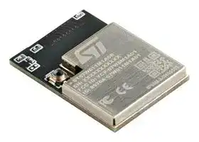


ST67W611M1A6PTR
Wi-Fi Combo Coprocessor Module, 802.11b/g/n/ax, Bluetooth v5.4, STM32, SPI/UART, 3.3V, 2.4 GHz
- Manufacturer: STMICROELECTRONICS
- Product type:
- SVHC: No SVHC (25-Jun-2025)
- Frequency RF: 2.4GHz
- Product Range: -
- Module Interface: SPI, UART
- Module Applications: Smart Home, Industrial IoT, Healthcare
| Delivery and price | |
|---|---|
| Units per pack | 250 |
| Price | 4.65 € |
| Current stock | 100+ |
| Lead time | 30 days |
**ST67W611M1**

Datasheet

Low-power Wi-Fi 6 - Bluetooth[®] LE combo coprocessor module

## **Features**

## **Module content**

- All-in-one Wi ‑ Fi[®] /Bluetooth[®] LE wireless microcontroller

- Embedded 40 MHz high-precision crystal

- All RF components for transmission and reception matching network, including antenna filter

- Three variants: embedded antenna (-B version), RF connector (-U version), RF pin (-P version)

## **Standard**

- IEEE 802.11b/g/n/ax

- Bluetooth[®] LE 5.4

- Regulatory certifications: CE/RED, UKCA, FCC, IC, JRF/ARIB, ACMA/RSM, RCM, BIS/WPC, NBTC, RoHS, REACH

**Product status** ST67W611M1

- Wi-Fi and Bluetooth LE can run concurrently dynamically

## **Wi-Fi**

• Wi-Fi 6, 2.4 GHz RF transceiver Wi-Fi 20/40 MHz bandwidth, 1T1R Wi-Fi security WPS/WEP/WPA/WPA2/WPA3

- STA, SoftAP, concurrent STA + SoftAP

- Maximum Tx power (11b 1 Mbps): 21 dBm

- Tx power (HE40 and MCS9): 16 dBm

- Rx sensitivity (HE40 and MCS9): -67 dBm

- Application throughput up to 17 Mbps (TCP)

- LDPC, STBC, beamforming, DL/UL OFDMA, MU-MIMO, target wake time (TWT), spatial reuse (SR), dual carrier modulation (DCM), extended range (ER)

- A-MPDU, A-MSDU, immediate block ACK, fragmentation, and defragmentation

## **Bluetooth[®] LE**

- Maximum Tx power: + 10 dBm

- Rx sensitivity

   -

   -

- Bluetooth[®] LE (2 Mbps): -96.5 dBm

- Bluetooth[®] LE (1 Mbps): -99 dBm

## **System peripherals**

- SPI

- UART

## **Security**

- PSA Level 1 certified

- Security system encryption engine

- Secure services: Secure boot and FOTA (firmware over-the-air)

**DS14784** - **Rev 4** - **September 2025** For further information, contact your local STMicroelectronics sales office.

www.st.com

**ST67W611M1**

## **Voltage**

- Input voltage: 3.3 V

- I/O voltage: 1.8 V/3.3 V

## **Environmental specifications**

- Temperature: – Operating: -40°C ~ +85°C

- – Storage: -40°C ~ +125°C

- • Humidity:

   - Relative: < 90% noncondensing

   - Storage: < 90% noncondensing

## **All packages are ECOPACK2 compliant.**

## **Application**

- Smart homes: – Door lock and door-bells – Cameras – Smart hub

- Industrial IoT:

   - Industrial control IoT hub/gateways

   - – Smart utility metering

   - EV chargers

- Smart appliances:

   - White goods

– Kitchen appliances

- Healthcare:

   - Portable patient monitors

   - Handled devices

**DS14784** - **Rev 4**

**page 2/37**

**ST67W611M1 Introduction**

**1 Introduction**

This document provides information on ST67W611M1 modules, such as description, pin assignment and definition, electrical characteristics, packaging and ordering information.

**DS14784** - **Rev 4**

**page 3/37**

**ST67W611M1 Description**

## **2 Description**

‑ ‑ Powered by Qualcomm high performance 1 × 1 2.4 GHz Wi Fi 6 and Bluetooth 5.4 modem, the STMicroelectronics ST67W611M1 LGA module is purposely designed to pack processing capabilities, Wi-Fi and ‑ ‑ Bluetooth LE combo connectivity, and on module memory into a single 32 pin LGA form factor.

This all ‑ in-one design and capability contribute to reduced costs and enhanced performance, making it an ‑ attractive choice for IoT edge devices requiring a single chip solution.

ST67W611M1 operates as an IoT connectivity transceiver, with an external STM32 host MCU running applications.

ST67W611M1 integrates:

- A PCB antenna (version -B), a RF connector (version-U) for external antenna, or version with a dedicated RF pin typically for support of multi-antenna implementations with external RF switch

- 4 MB NOR flash

- 40 MHz high-precision quartz for optimal RF performance

- SMPS functionality and associated bill of material (BOM)

- All needed discrete components to reduce the overall board BOM

- Data interface through SPI

- 32768 Hz internal oscillator. For low-power use cases, two pins are provided to use a 32768 Hz quartz. One pin can also be used to receive an accurate 32768 Hz from the host processor.

In addition, the P variant supports:

- External PA/LNA to increase power up to 30 dBm

- Rx antenna diversity to increase the reach of your final product using several antennas.

Figure 1 shows the general block diagram of the device family.

## **Figure 1. ST67W611M1 block diagram**

RF (embedded or external through connectors/pin)

**==> picture [337 x 170] intentionally omitted <==**

**----- Start of picture text -----**<br>
RF front end<br>Wi-Fi 6 Bluetooth® LE<br>PHY and MAC PHY and MAC<br>32 kHz (optional)<br>CPU, security and memory<br>Boot<br>4 MB  40 MHz SPI and<br>Power management<br>flash xtal UART<br>ST67W611M1<br>Data Enable<br>**----- End of picture text -----**<br>


## **2.1**

## **UART interface**

The UART interface uses two pins (Rx and Tx) and is configured as follows:

- Full-duplex asynchronous communication

- Data bit length: 8 bits

- Stop bit length: 1 bit

- Parity: None

- Hardware flow control (RTS/CTS): None

- Baud rate: 2000000 bauds

**DS14784** - **Rev 4**

**page 4/37**

**ST67W611M1 Description**

## **2.2 SPI interface**

The SPI bus is configured in full-duplex slave mode with three signals (SPI_CLK, SPI_MOSI, SPI_MISO). The SPI_RDY pin is present and used by the ST67W611M1 as an interrupt towards the host processor. The SPI_CS pin can also be used as a wake-up signal from the host processor. Maximum SPI frequency : 40 MHz.

**DS14784** - **Rev 4**

**page 5/37**

**ST67W611M1 Pinouts and pin description**

**3 Pinouts and pin description**

## **3.1 Pinout schematics**

## **Figure 2. ST67W611M1A6B LGA module PCB antenna**

Bottom view

**==> picture [241 x 244] intentionally omitted <==**

**----- Start of picture text -----**<br>
SPI_CS 24 1 RESERVED<br>UART_RX 23 2 RESERVED<br>UART_TX 22 GND GND 3 BOOT<br>SPI_RDY 21 4 RESERVED<br>RESERVED 20 5 RESERVED<br>RESERVED 19 GND GND 6 RESERVED<br>GND 18 7 RESERVED<br>CHIP_EN 17 8 RESERVED<br>VDDIO GND SPI_MOSI SPI_CLK SPI_MISO GND NC GND<br>VDD33 GND XTAL32K_IN XTAL32K_OUT RESERVED RESERVED GND VDDIO<br>25 26 27 28 29 30 31 32<br>16 15 14 13 12 11 10 9<br>**----- End of picture text -----**<br>


## **Figure 3. ST67W611M1A6U LGA module antenna connector**

**==> picture [242 x 265] intentionally omitted <==**

**----- Start of picture text -----**<br>
Bottom view<br>SPI_CS 24 1 RESERVED<br>UART_RX 23 2 RESERVED<br>UART_TX 22 GND GND 3 BOOT<br>SPI_RDY 21 4 RESERVED<br>RESERVED 20 5 RESERVED<br>RESERVED 19 GND GND 6 RESERVED<br>GND 18 7 RESERVED<br>CHIP_EN 17 8 RESERVED<br>VDDIO GND SPI_MOSI SPI_CLK SPI_MISO GND NC GND<br>VDD33 GND XTAL32K_IN XTAL32K_OUT RESERVED RESERVED GND VDDIO<br>25 26 27 28 29 30 31 32<br>16 15 14 13 12 11 10 9<br>**----- End of picture text -----**<br>


**DS14784** - **Rev 4**

**page 6/37**

**ST67W611M1 Pinouts and pin description**

**Figure 4. ST67W611M1A6P LGA module pin connector**

Bottom view

**==> picture [326 x 246] intentionally omitted <==**

**----- Start of picture text -----**<br>
|||||||
|---|---|---|---|---|---|
|SPI_CS|24|1|ANT_SEL|
|UART_RX|23|2|RESERVED|
|UART_TX|22|GND|GND|3|BOOT|
|SPI_RDY|21|4|RESERVED|
|RESERVED|20|5|RESERVED|
|RESERVED|19|GND|GND|6|RESERVED|
|GND|18|7|RESERVED|
|CHIP_EN|17|8|RESERVED|

**----- End of picture text -----**<br>


**DS14784** - **Rev 4**

**page 7/37**

**ST67W611M1 Pinouts and pin description**

## **3.2 Pin description**

**Table 1. ST67W611M1 pin definition**

|**Pin number**|**Pin name**|**Pin type **|**Power domain**|**Description**|
|---|---|---|---|---|
|1|RESERVED(1)<br>ANT_SEL|I/O|VDDIO|RESERVED: ST67W611M1A6B and ST67W611M1A6U<br>ANT_SEL: ST67W611M1A6P|
|2|RESERVED(1)|I/O|VDDIO|-|
|3|BOOT|I/O|VDDIO|Select boot from SPI or from UART.|
|4|RESERVED(1)|I/O|VDDIO|-|
|5|RESERVED(1)|I/O|VDDIO|-|
|6|RESERVED(1)|I/O|VDDIO|-|
|7|RESERVED(1)|I/O|VDDIO|-|
|8|RESERVED(1)|I/O|VDDIO|-|
|9|VDDIO|PWR|-|Host I/O voltage input (3.3 V or 1.8 V)|
|10|GND|GND|GND|Ground|
|11|RESERVED(1)|I/O|VDDIO|-|
|12|RESERVED(1)|I/O|VDDIO|-|
|13|XTAL32K_OUT|I/O|VDD33|32.768 kHz quartz is optional. 32.768 kHz coming from host processor can be<br>provided on this pin.|
|14|XTAL32K_IN|I/O|VDD33|32.768 kHz quartz is optional.|
|15|GND|GND|GND|Ground|
|16|VDD33|PWR|-|Power input (3.3 V)|
|17|CHIP_EN|DI|-|Chip power on|
|18|GND|GND|GND|Ground|
|19|RESERVED(1)|I/O|VDDIO|-|
|20|RESERVED(1)|I/O|VDDIO|-|
|21|SPI_RDY|I/O|VDDIO|Data ready to be transmitted to host processor.|
|22|UART_TX|I/O|VDDIO|UART Tx line from ST67W611M1 point of view.|
|23|UART_RX|I/O|VDDIO|UART Rx line from ST67W611M1 point of view.|
|24|SPI_CS|I/O|VDDIO|Input of the SPI slave-select from the SPI master/host.|
|25|VDDIO|PWR|-|Host I/O voltage input (3.3 V or 1.8 V)|
|26|GND|GND|GND|Ground|
|27|SPI_MOSI|I/O|VDDIO|Input SPI data from the master/host to the module.|
|28|SPI_CLK|I/O|VDDIO|Input of SPI clock signal generated by the SPI master/host.|
|29|SPI_MISO|I/O|VDDIO|Output of SPI data from the module to the SPI master/host.|
|30|GND|GND|GND|Ground|
|31|NC<br>RF|-<br>RF|-|NC: ST67W611M1A6B and ST67W611M1A6U<br>RF: ST67W611M1A6P|
|32|GND|GND|GND|Ground|


_1. RESERVED pins must be left NC._

**DS14784** - **Rev 4**

**page 8/37**

**ST67W611M1 Electrical characteristics**

## **4 Electrical characteristics**

## **4.1 Absolute maximum ratings**

The absolute maximum ratings provided in this section indicate the stress levels that, if exceeded, may result in permanent damage to the device. Functionality outside the specified operating conditions is not guaranteed. Both functionality and reliability are guaranteed only within the defined operating specifications.

**Table 2. Absolute maximum ratings**

|**Pin name**|**Min.**|**Max.**|**Unit**|
|---|---|---|---|
|VDD33|-0.3|3.63|V|
|VDDIO|-0.3|3.63||
|TS(storage temperature)(1)(2)|-40|+125|°C|


_1. The storage temperature range applies when the device is in the off state (the device is not assembled in any platform and is not electrically connected to any voltage or I/O signals). Damage may occur when the device is subjected to this temperature for any length of time._

_2. For devices shipped in tape and reel, the storage temperature range is [+15 °C +35 °C] and < 90 % relative humidity (RH). ST recommends allowing the device to return to ambient room temperature before usage._

## **4.2 Electrical sensitivity characteristics**

**Table 3. Electrical sensitivity characteristics**

|**Tests, standards, and conditions**|**Result**|
|---|---|
|ESD contact discharge (IEC 61000-4-2)|2 kV pass|
|ESD protection (HBM)|2 kV|


## **4.3**

## **Operating conditions**

Operating conditions include controlled parameters such as power supply voltage, power distribution impedances, and thermal conditions. The ST67W611M1 meets all performance specifications when used within the operating conditions, unless otherwise noted in those sections (provided the absolute maximum ratings have never been exceeded).

**Table 4. Recommended power operating range**

|**Pin name**|**Min.**|**Typ**|**Max.**|**Unit**|
|---|---|---|---|---|
|VDD33|2.97|3.3|3.63|V|
|VDDIO|1.65|3.3 or 1.8|3.6||


**Table 5. Recommended temperature operating range**

|**Item**|**Min.**|**Max.**|**Unit**|
|---|---|---|---|
|Ambient temperature|-40|85|°C|


**DS14784** - **Rev 4**

**page 9/37**

**ST67W611M1 Electrical characteristics**

## **4.4**

## **Power-on sequence**

To ensure normal power-on startup, the power, reset, and bootstrap pins must meet the corresponding timing requirements.

## **Figure 5. Power-on sequence**

**==> picture [33 x 226] intentionally omitted <==**

**----- Start of picture text -----**<br>
(1)<br>POR<br>(40 MHz)<br>**----- End of picture text -----**<br>


(1) VDD33 and VDDIO can be independent. Both must have reached there minimal value to start communication with host.

**Table 6. Power-on sequence parameters**

|**Parameters**|**Description**|**Min.**<br>**(ms)**|**Typ**<br>**(ms)**|**Max.**<br>**(ms)**|
|---|---|---|---|---|
|t0|The power supply voltage reaches 90% rise time(1)|-|0.1|-|
|t1|Internal POR duration|-|3|-|
|t2|VDDCORE setting time after internal POR down|-|1|-|
|t3.1|Bootstrap pin(2)preparation time before VDDCORE establishment|0|-|-|
|t3.2|Duration of valid voltage level at the bootstrap pin.|2|-|-|
|t4|XTAL startup time after internal POR down|-|1|-|


_1. The timing value applies both to VDD33 and VDDIO for proper chip operation._

_2. The bootstrap pin is BOOT._

**DS14784** - **Rev 4**

**page 10/37**

**ST67W611M1 Electrical characteristics**

## **4.5 Shutdown sequence**

**Figure 6. Shutdown sequence**

**==> picture [55 x 244] intentionally omitted <==**

**----- Start of picture text -----**<br>
VDD33<br>VDDIO<br>PU_CHIP<br>Internal POR<br>VDDCORE<br>Bootstrap<br>XTAL (40 MHz)<br>**----- End of picture text -----**<br>


**Table 7. Shutdown sequence parameters**

|**Parameters**|**Description**|**Min.**|**Typ**|**Max.**|**Unit**|
|---|---|---|---|---|---|
|VRST|Shutdown occurs after PU_CHIP lower than this voltage|0|0.1 × VDD33|0.3 × VDD33|V|
|tRST|The required time that PU_CHIP lower than VRST|1|1|-|ms|
|tpd|Time for VDDCORE to decrease to 0 after shutdown|1|1|-|ms|


## **4.6 DC power characteristics**

Test conditions: VDDIO = 3.3 V, temperature = 25 °C

**Table 8. I/O DC characteristics**

|**Symbol**|**Description**|**Min.**|**Typ**|**Max.**|**Unit**|
|---|---|---|---|---|---|
|VOH|Output voltage high|-|0.9 × VDDIO|-|V|
|VOL|Output voltage low|-|0.1 × VDDIO|-||
|VIH|Input voltage high|0.7 × VDDIO|-|-||
|VIL|Input voltage low|-|-|0.3 × VDDIO||


**DS14784** - **Rev 4**

**page 11/37**

**ST67W611M1 Electrical characteristics**

## **4.7 WLAN RF characteristics**

**Table 9. 802.11b/g/n/ax radio performance**

|**Standard**|**PHY**|**Modulation**|**MCS Index**|**Max Tx Power (dBm)(1)**|**Max Tx Power (dBm)(1)**|**Rx Sensitivity (dBm)**|**Rx Sensitivity (dBm)**|
|---|---|---|---|---|---|---|---|
|||||**20 MHz**|**40 MHz**|**20 MHz**|**40 MHz**|
|802.11b|CCK (DSSS)|DBPSK|–|21|–|-99|–|
||CCK (DSSS)|DQPSK|–|21|–|-96|–|
||CCK (DSSS)|B/DQPSK|–|21|–|-93.5|–|
||CCK (DSSS)|Q/DQPSK|–|21|–|-90.5|–|
|802.11g|OFDM|BPSK|–|20|–|-93.5|–|
||OFDM|BPSK|–|20|–|-93|–|
||OFDM|QPSK|–|20|–|-92|–|
||OFDM|QPSK|–|20|–|-89.5|–|
||OFDM|16 QAM|–|20|–|-87|–|
||OFDM|16 QAM|–|20|–|-83.5|–|
||OFDM|64 QAM|–|18|–|-79|–|
||OFDM|64 QAM|–|18|–|-78|–|
|802.11n|OFDM|BPSK|MCS0|19|18.5|-93|-90|
||OFDM|QPSK|MCS1|19|18.5|-91|-88|
||OFDM|QPSK|MCS2|19|18.5|-88.5|-85.5|
||OFDM|16 QAM|MCS3|19|18.5|-86|-83.5|
||OFDM|16 QAM|MCS4|19|18.5|-82.5|-79.5|
||OFDM|64 QAM|MCS5|18.5|18|-78.5|-75.5|
||OFDM|64 QAM|MCS6|18.5|18|-76.5|-74|
||OFDM|64 QAM|MCS7|18|17|-75.5|-72.5|
|802.11ax|OFDMA|BPSK|MCS0|19|19|-93.5|-90.5|
||OFDMA|QPSK|MCS1|19|19|-92.5|-89.5|
||OFDMA|QPSK|MCS2|19|19|-90|-87.5|
||OFDMA|16 QAM|MCS3|19|19|-87.5|-84.5|
||OFDMA|16 QAM|MCS4|19|19|-84|-81.5|
||OFDMA|64 QAM|MCS5|18.5|18|-80|-77|
||OFDMA|64 QAM|MCS6|18|18|-79|-76|
||OFDMA|64 QAM|MCS7|18|17|-78|-75|
||OFDMA|256 QAM|MCS8|18|17|-73|-70.5|
||OFDMA|256 QAM|MCS9|17|16|-72|-69.5|


_1. The maximum power ratings reflect the transmitter’s maximum power capability and is region-dependent. Refer to the specific certificate associated to the region for exact maximum output power._

**Table 10. Bluetooth LE performance**

|**Standard**|**Topology**|**PHY**|**Modulation**|**Data Rate**|**Max Tx Power (dBm)**|**Rx Sensitivity (dBm)**|
|---|---|---|---|---|---|---|
|BLE|P2P Broadcast Mesh|LE 2M|GFSK|2Mbps|+10|-97|
|||LE 1M|GFSK|1Mbps|+10|-99|


**DS14784** - **Rev 4**

**page 12/37**

**ST67W611M1 Electrical characteristics**

|**Standard**|**Topology**|**PHY**|**Modulation**|**Data Rate**|**Max Tx Power (dBm)**|**Rx Sensitivity (dBm)**|
|---|---|---|---|---|---|---|
|BLE|P2P Broadcast Mesh|LE Coded (S=2)|GFSK|500 Kbps|+10|-102|
|||LE Coded (S=8)|GFSK|125 Kbps|+10|-105|


**Table 11. Synthesizer composite characteristics and transmit output power accuracy**

|**Symbol**|**Parameter**|**Conditions**|**Min.**|**Typ**|**Max.**|**Unit**|
|---|---|---|---|---|---|---|
|**Synthesizer composite characteristics for 2.4 GHz**|||||||
|Fc|Center channel frequency|Center frequency at 5 MHz<br>spacing|2412|-|2484|MHz|
|Fref|Reference oscillator frequency|±20 ppm|-|40|-|MHz|
|Fstep|Frequency step size (at RF)|-|-|5|-|MHz|
|TSPOWERUP|Time for power-up (from sleep)|-|-||50|us|
|**Transmit output power accuracy**|||||||
|APC(1)|Accuracy of transmit power control at 2.4 GHz at<br>room temperature (3 sigma over top 10 dB of TPC<br>range).|OLPC (Open Loop Power<br>Control)|-|±1.5|-|dB|


_1. All APC numbers assume conducted test with 50 Ω load._

## **4.8**

## **Power consumption**

- **Active** : Continuous transmitting or receiving on connection to access point (AP).

- **DeepSleep** : Digital and analog parts are mostly powered off. RAM is in retention. This is the DTIM power ‑ saving mode.

- **Shutdown** : The chip is supplied but in shut down.

The power consumption for each state is listed in the table below:

**Table 12. Power consumption at 3.3 V, 25 °C**

|**Operation mode**|**State**|**Typ**|**Unit**|**Comments**|
|---|---|---|---|---|
|||Static|||
|Power saving|DeepSleep|90|μA|Digital and analog parts are mostly powered off. RAM is in<br>retention. This is the DTIM power‑saving mode.|
||Shutdown|0.2||-|
|||DTIM|||
|DTIM|DTIM1|720|μA|Ext32k|
|||720||Xtal32k|
|||830||RC32k|
||DTIM3|300||Ext32k|
|||300||Xtal32k|
|||390||RC32k|
||DTIM5|240||Ext32k|
|||240||Xtal32k|
|||290||RC32k|
||DTIM10|130||Ext32k|
|||130||Xtal32k|
|||180||RC32k|


**DS14784** - **Rev 4**

**page 13/37**

**ST67W611M1 Electrical characteristics**

## **TWT current consumption**

The measurements are done in TWT mode between the ST67W611M1 and a commercialized Wi-Fi 6 access point.

The following TWT current consumption measurements are done on an X-NUCLEO board which has an average current consumption of 90 μA when there is no activity (that is, in deepsleep during TWT doze state and while there is no `hcp_coarse_tmr` or probe request activity). Current consumption measurements are done after the initial phase of the probe requests. On STA side, TWT starts with several probe requests to gather AP timing data necessary for precise TWT wakeups.

**Table 13. TWT current consumption**

|**Mode**|**Average Current consumption**<br>**SP = 32ms**|**Average Current consumption**<br>**SPmax = 64ms**|**Unit**|
|---|---|---|---|
|TWT 1 s|2786.2|4778.5|uA|
|TWT 10 s|363.4|552.5|uA|
|TWT 20 s|229.4|335.5|uA|
|TWT 30 s|183.8|218.5|uA|
|TWT 1 min|152.5|171|uA|
|TWT 5 min|111.5|115.5|uA|
|TWT 10 min|105.2|109.5|uA|
|TWT 20 min|103.8|104.8|uA|
|TWT 30 min|103.4|102.8|uA|
|TWT 1 h|103.4|102.7|uA|


**Table 14. Power consumption for continuous WLAN Tx 2.4 GHz at 3.3 V, 25 °C**

|**Rate**|**Power (dBm)**|**Current consumption (mA)**|
|---|---|---|
|11b 1 Mbps|22|372|
|11b 11 Mbps|22|377|
|11g 6 Mbps|21|352|
|11g 54 Mbps|19|304|
|MCS0 HT20|20|326|
|MCS7 HT20|19|311|
|MCS0 HT40|19|310|
|MCS7 HT40|18|292|
|MCS0 HE20|20|317|
|MCS9 HE20|18|285|
|MCS0 HE40|20|321|
|MCS9 HE40|16|262|


**Table 15. Power consumption for continuous WLAN Rx 2.4 GHz at 3.3 V, 25 °C**

|**Rate**|**Current consumption (mA)**|
|---|---|
|11b 1 Mbps|55|
|11b 11 Mbps|56|
|11g 6 Mbps|59|


**DS14784** - **Rev 4**

**page 14/37**

**ST67W611M1 Electrical characteristics**

|**Rate**|**Current consumption (mA)**|
|---|---|
|11g 54 Mbps|62|
|MCS0 HT20|59|
|MCS7 HT20|63|
|MCS0 HT40|71|
|MCS7 HT40|78|
|MCS0 HE20|60|
|MCS9 HE20|65|
|MCS0 HE40|74|
|MCS9 HE40|77|


**Table 16. Power consumption for Bluetooth[®] LE at 3.3 V, 25 °C**

|**Description**|**Current consumption (mA)**|
|---|---|
|Continuous Rx burst|53|
|Continuous Tx (+4 dBm)|107|
|Continuous Tx (+10 dBm)|167|
|1.28 sec page scan (non-interlaced)|0.75|
|1.28 sec LE ADV|0.32|


**DS14784** - **Rev 4**

**page 15/37**

**ST67W611M1 Mechanical information**

## **5**

## **Mechanical information**

## **5.1 Device physical dimensions**

## **5.1.1 ST67W611M1 LGA module PCB antenna (-B version)**

**Figure 7. ST67W611M1 LGA module PCB antenna dimension**

**==> picture [36 x 6] intentionally omitted <==**

**----- Start of picture text -----**<br>
2.37mm max<br>**----- End of picture text -----**<br>


**==> picture [5 x 33] intentionally omitted <==**

**----- Start of picture text -----**<br>
DT75611V2<br>**----- End of picture text -----**<br>


**Figure 8. ST67W611M1 LGA module PCB antenna landing pad**

**DS14784** - **Rev 4**

**page 16/37**

**ST67W611M1 Mechanical information**

## **5.1.2 ST67W611M1 LGA module antenna connector (-U version)**

**Figure 9. ST67W611M1 LGA module antenna connector dimension**

**==> picture [36 x 5] intentionally omitted <==**

**----- Start of picture text -----**<br>
2.37mm max<br>**----- End of picture text -----**<br>


**==> picture [5 x 33] intentionally omitted <==**

**----- Start of picture text -----**<br>
DT75613V2<br>**----- End of picture text -----**<br>


**Figure 10. ST67W611M1 LGA module antenna connector landing pad**

**DS14784** - **Rev 4**

**page 17/37**

**ST67W611M1 Mechanical information**

## **5.1.3 ST67W611M1 LGA module RF pin (-P version)**

**Figure 11. ST67W611M1 LGA module RF pin dimension**

**Figure 12. ST67W611M1 LGA module RF pin landing pad**

**DS14784** - **Rev 4**

**page 18/37**

**ST67W611M1 Manufacturing guidelines**

## **6 Manufacturing guidelines**

## **6.1 Power layout guideline**

The ST67W611M1 can be powered by either a battery or a DC 3.3 V power supply. To ensure proper operation, follow these guidelines for power pin connections and decoupling:

1. Place the capacitor as close as possible to the chip and the power pin.

2. Use a capacitor to decouple the power supply from the chip.

3. Use capacitors to prevent noise from coupling back to the power plane.

**Figure 13.  Power layout guideline**

## **6.2**

## **RF layout guideline**

To optimize antenna performance, follow these guidelines for placing ST67W611M1 on the PCB:

1. Place ST67W611M1 in the corner of the PCB as shown in Figure 14.

2. Do not cover the antenna clearance area with copper or traces.

3. Keep the antenna area as far away as possible from the power supply and metal components.

4. Connect all GND pins directly to a solid GND plane.

5. Place GND vias as close as possible to the GND pin.

6. Use a good layout method to avoid excessive noise coupling with signal lines or supply voltage lines.

## **Figure 14.  RF layout guideline**

**DS14784** - **Rev 4**

**page 19/37**

**ST67W611M1 Manufacturing guidelines**

## **6.3 Soldering guideline**

ST67W611M1 can be SMT on the board following the temperature curve graph.

**Figure 15.  Soldering guideline**

**DS14784** - **Rev 4**

**page 20/37**

**ST67W611M1 Tape and reel information**

## **7 Tape and reel information**

All tape carrier systems conform to EIA-481 standards.

The following figure shows the simplified sketch of the ST67W611M1 tape carrier including the part orientation, maximum number of devices per reel, and key dimensions

**Figure 16. Carrier tape drawing with part orientation**

**==> picture [5 x 33] intentionally omitted <==**

**----- Start of picture text -----**<br>
DT77579V1<br>**----- End of picture text -----**<br>


## **Table 17. ST67W611M1A6B**

||**Table 17. ST67W611M1A6BST67W611M1A6B**||
|---|---|---|
|Tape feed: Single|Reel diameter: 330 mm|Tape width: 32 mm|
|Units per reel: 800|Hub diameter: 178 mm|Pocket pitch: 20 mm|


## **Table 18. ST67W611M1A6U / ST67W611M1A6P**

|Tape feed: Single|Reel diameter: 330 mm|Tape width: 24 mm|
|---|---|---|
|Units per reel: 800|Hub diameter: 178 mm|Pocket pitch: 20 mm|


The following figure shows the tape-handling recommendation.

## **Figure 17. Tape handling**

**==> picture [5 x 33] intentionally omitted <==**

**----- Start of picture text -----**<br>
DT77580V1<br>**----- End of picture text -----**<br>


**DS14784** - **Rev 4**

**page 21/37**

**ST67W611M1 Device moisture sensitivity level**

## **8 Device moisture sensitivity level**

A package’s moisture sensitivity level (MSL) indicates its ability to withstand exposure after it is removed from its shipment bag, while it is on the factory floor awaiting PCB installation. A low MSL rating is better than a high rating; a low MSL device can be exposed on the factory floor longer than a high MSL device. All pertinent MSL ratings are summarized in Table 19.

**Table 19. MSL ratings summary**

|**MSL**|**Out-of-bag floor life**|**Comments**|
|---|---|---|
|1|Unlimited|≤ 30°C/85% RH|
|2|1 year|≤ 30°C/60% RH|
|2a|4 weeks|≤ 30°C/60% RH|
|3|168 hours|≤ 30°C/60% RH; ST67W611M1|
|4|72 hours|≤ 30°C/60% RH|
|5|48 hours|≤ 30°C/60% RH|
|5a|24 hours|≤ 30°C/60% RH|
|6|Mandatory bake before use. After baking, it must be reflowed within the time limit<br>specified on the label.|≤ 30°C/60% RH|


ST follows the latest IPC/JEDEC J-STD-020 standard revision for moisture-sensitivity qualification. The ST67W611M1 devices are targeted as MSL3.

**DS14784** - **Rev 4**

**page 22/37**

**ST67W611M1 Bagged storage conditions**

## **9 Bagged storage conditions**

ST67W611M1 devices delivered in tape and reel carriers must be stored in sealed, moisture barrier, antistatic bags.

**DS14784** - **Rev 4**

**page 23/37**

**ST67W611M1 Handling**

## **10 Handling**

Tape handling is described in Tape and reel information. For other (IC-specific) handling guidelines, see the following topics.

## **10.1 Baking**

It is not necessary to bake the ST67W611M1 if the conditions specified in Bagged storage conditions and Out-ofbag duration have not **been exceeded** .

It is necessary to bake the ST67W611M1 if any condition specified in Bagged storage conditions or Out-of-bag duration has **been exceeded** . The baking conditions are specified on the moisture-sensitive caution label attached to each bag.

## **Caution:**

_If baking is required, the devices must be transferred into trays that can be baked to at least 125°C. Do not bake devices in tape and reel carriers at any temperature._

## **10.2 Electrostatic discharge**

Electrostatic discharge (ESD) occurs naturally in laboratory and factory environments. An established highvoltage potential is always at risk of discharging to a lower potential. If this discharge path is through a semiconductor device, destructive damage may result. ESD countermeasures and handling methods must be developed and used to control the factory environment at each manufacturing site.

**DS14784** - **Rev 4**

**page 24/37**

**ST67W611M1 Ordering information**

## **11 Ordering information**

Example: ST67 W 6 1 1 M 1 A 6 B/P/U TR

## **Device family**

ST67 = ST RFOC Connectivity product

## **Product type**

W = Wi-Fi

## **Device subfamily**

6 = Wi-Fi6 version

## **Flash memory size**

1 = Side-by-side flash

## **Data interface**

1 = SPI

## **Component type**

M = Module

## **Hardware feature set**

1 = Without 32 KHz Xtal

## **Package**

A = PCB version A

## **Temperature range**

6 = Industrial temperature range,

– 40 °C to 85 °C

## **Options**

B = PCB antenna

P = Pinned

U = MHF4 antenna connector

## **Packing**

TR = Tape and reel

**DS14784** - **Rev 4**

**page 25/37**

**ST67W611M1 FCC- ISED compliance statement**

## **12 FCC- ISED compliance statement**

## **FCC Part 15 compliance statement**

Changes or modifications not expressly approved by STMicroelectronics could void the user’s authority to operate the equipment.

This device complies with part 15 of the FCC Rules. Operation is subject to the following two conditions: (1) This device may not cause harmful interference, and (2) this device must accept any interference received, including interference that may cause undesired operation.

FCCID: YCP-67W611M1A01

Product Marketing Name: ST67W611M1A

Models Name: ST67W611M1A

- Applicable FCC rules: Thismodule has been approved under FCC part 15C 15.247 in the frequency range 2400-2483.5MHz. This modular transmitter is only FCC authorized for this specific rule part.

- Specific operational use conditions:

   - The module is limited to OEM installation ONLY.

   -

      - Only the module grantee is permitted to make permissive changes.

   - The OEM integrator is responsible for ensuring that the end-user has no manual instruction to remove or install module.

- Limited module procedures are not applicable to this application.

- Trace antenna: Not applicable

- Radio Frequency (RF) Exposure Compliance of Radio communication: To satisfy FCC RF Exposure requirements, a separation distance of 20cm or more should be maintained between the antenna of this device and persons during operation. To ensure compliance, operation at a closer distance than this is not recommended. This transmitter must not be co- located or operating in conjunction with any other antenna or transmitter.

- List of antenna type approved for ST67W611M1A6U & ST67W611M1A6P:

   - External PIFA, max antenna gain: 3.19dBi

   - External dipole, max antenna gain: 3.37dBi

   -

      - External monopole, max antenna gain: 3.12dBi

      - If other antenna with higher gain or other antennas type, other than the type documented in the filing, a class 2 permissive change must be filed with FCC

- End Product Labeling: The final end product must be labeled in a visible area with the following: _“Contains Transmitter Module FCC ID: YCP-67W611M1A01”_

- End Product User’s Manual: The user manual for end users must include the following information in a prominent location: _To satisfy FCC RF Exposure requirements, a separation distance of 20cm or more should be maintained between the antenna of this device and persons during operation. To ensure compliance, operation at a closer distance than this is not recommended. This transmitter must not be colocated or operating in conjunction with any other antenna or transmitter._

- Additional testing requirements:

   - If testing of the host product with this transmitter installed and operating is necessary (to verify that the host product meets all the applicable FCC rules), a test mode for this specific module is available upon request to STMicroelectronics.

- The host product manufacturer is responsible for compliance to any other FCC rules that apply to the host not covered by the modular transmitter grant of certification. (For example, Part 15 Subpart B)

## **ISED- Industry Canada Licence-Exempt Radio Apparatus**

IC: 8976A-67W611M1A01

Product Marketing Name: ST67W611M1A

HVIN: ST67W611M1A6B & ST67W611M1A6U & ST67W611M1A6P

Note: ST67W611M1A6B & ST67W611M1A6U & ST67W611M1A6P models share this same user’s manual because these two models belong to the same hardware family of the ST67W611M1A module.

**DS14784** - **Rev 4**

**page 26/37**

**ST67W611M1 FCC- ISED compliance statement**

This device contains licence-exempt transmitter(s)/receivers(s) that comply with Innovation, Science and EconomicDevelopment Canda’s licence-exempt RSS(s). Operation is subject to the following two conditions:

1. This device may not cause interference

2. This device must accept any interference, including interference that may cause undesired operation of the device.

- Applicable ISED-CANADA rules: Thismodule has been approved under RSS-247 in the frequency range 2400-2483.5MHz. This modular transmitter is only ISED authorized for this specific rule part.

- Specific operational use conditions:

   - The module is limited to OEM installation ONLY.

   - Only the module grantee is permitted to make permissive changes.

   - The OEM integrator is responsible for ensuring that the end-user has no manual instruction to remove or install module.

- Limited module procedures are not applicable to this application.

- Trace antenna: Not applicable.

- Radio Frequency (RF) Exposure Compliance of Radio communication: To satisfy ISED-Canada RF Exposure requirements, a separation distance of 20cm or more should be maintained between the antenna of this device and persons during operation. To ensure compliance, operation at a closer distance than this is not recommended. This transmitter must not be co- located or operating in conjunction with any other antenna or transmitter.

- This radio transmitter IC: 8976A-67W611M1A01 has been approved by Innovation, Science and Economic Development Canada to operate with the antenna types listed below, with the maximum permissible gain indicated. Antenna types not included in this list that have a gain greater than the maximum gain indicated for any type listed are strictly prohibited for use with this device.

List of antenna type approved for ST67W611M1A6U & ST67W611M1A6P:

   - External PIFA, max antenna gain: 3.19dBi

   - External dipole, max antenna gain: 3.37dBi

   - External monopole, max antenna gain: 3.12dBi

   - If other antenna with higher gain or other antennas type, other than the type documented in the filing, a class 2 permissive change must be filed with ISED-Canada.

- End Product Labeling: The final end product must be labeled in a visible area with the following: _Contains Transmitter Module IC: 8976A-67W611M1A01”_

- End Product User’s Manual: The user manual for end users must include the following information in a prominent location: _To satisfy ISED-Canada RF Exposure requirements, a separation distance of 20cm or more should be maintained between the antenna of this device and persons during operation. To ensure compliance, operation at a closer distance than this is not recommended. This transmitter must not be colocated or operating in conjunction with any other antenna or transmitter_ .

- Additional testing requirements: If testing of the host product with this transmitter installed and operating is necessary (to verify that the host product meets all the applicable ISED-Canada rules), a test mode for this specific module is available upon request to STMicroelectronics.

- The host product manufacturer is responsible for compliance to any other ISED-Canada rules that apply to the host not covered by the modular transmitter grant of certification. (For example, ICES-003)

## **ISED- Industry Canada Licence-Exempt Radio Apparatus**

IC: 8976A-67W611M1A01

Nom de marque du produit: ST67W611M1A

NIVM: ST67W611M1A6B & ST67W611M1A6U & ST67W611M1A6P

Remarque : les modèles ST67W611M1A6B & ST67W611M1A6U & ST67W611M1A6P partagent ce même manuel d'utilisation car ces deux modèles appartiennent à la même famille matérielle du module ST67W611M1A.

L’émetteur/récepteur exempt de licence contenu dans le présent appareil est conforme aux CNR d’Innovation, Sciences et Développement économique Canada applicables aux appareils radio exempts de licence. L’exploitation est autorisée aux deux conditions suivantes :

1. L’appareil ne doit pas produire de brouillage;

2. L’appareil doit accepter tout brouillage radioélectrique subi, même si le brouillage est susceptible d’en compromettre le fonctionnement.

**DS14784** - **Rev 4**

**page 27/37**

**ST67W611M1 FCC- ISED compliance statement**

- Règles ISED-CANADA applicables : Ce module a été approuvé suivant la norme RSS-247 dans la gamme de fréquences 2400-2483.5MHz. Cet émetteur modulaire est uniquement autorisé par ISDE pour cette partie de règle spécifique.

- Conditions opérationnelles spécifiques d'utilisation :

   - Le module est limité à l'installation OEM uniquement.

   - Seul le titulaire de la certification du module est autorisé à apporter des modifications permissives.

   - L'intégrateur OEM est responsable de s'assurer que l'utilisateur final ne dispose d'aucune instruction pour retirer ou installer le module.

- Les procédures de module limité ne sont pas applicables à cette application.

- Conception de la piste d’antenne : Non applicable

- Conformité des communications radio en matière d'exposition aux radiofréquences (RF) : Pour satisfaire aux exigences d'ISDE-Canada en matière d'exposition aux radiofréquences, une distance de séparation de 20 cm ou plus doit être maintenue entre l'antenne de cet appareil et les personnes pendant le fonctionnement. Pour assurer la conformité, il est déconseillé d'utiliser cet équipement à une distance inférieure. Cet émetteur ne doit pas être co-situé ou fonctionner conjointement avec une autre antenne ou un autre émetteur.

- Cet émetteur radio 8976A-67W611M1A01 a été approuvé par Innovation, Sciences et Développement Economique Canada pour fonctionner avec les types d'antennes énumérés ci-dessous, avec le gain maximal autorisé indiqué. Les types d'antennes non inclus dans cette liste, ou qui ont un gain supérieur au gain maximal indiqué pour tout type répertorié sont strictement interdits pour une utilisation avec cet appareil.

   - Liste des types d'antennes approuvés :

   - Antenna PIFA, gain maximal : 3.19dBi

   - Antenne dipole, gain maximal : 3.37dBi

   - Antenna monopole, gain maximal : 3.12dBi

Si d'autres antennes avec un gain plus élevé ou d'un autre type d'antenne, autre que le type documenté dans le dossier, un changement permissif de classe 2 doit être déposé auprès d'ISDE-Canada.

- Étiquetage du produit final : Le produit final doit être étiqueté dans une zone visible avec les éléments suivants : « Contient IC : 8976A-67W611M1A01 »

- Manuel de l'utilisateur du produit final : le manuel de l'utilisateur destiné aux utilisateurs finaux doit inclure les informations suivantes dans un endroit bien en vue : Pour satisfaire aux exigences d'ISDE-Canada en matière d'exposition aux RF, une distance de séparation de 20 cm ou plus doit être maintenue entre l'antenne de cet appareil et les personnes pendant le fonctionnement. Pour garantir la conformité, il n'est pas recommandé d'opérer à une distance plus courte que celle-ci. Cet émetteur ne doit pas être colocalisé ou fonctionner en conjonction avec une autre antenne ou émetteur.

- Exigences de tests supplémentaires : Si un test du produit hôte avec cet émetteur installé et opérationnel est nécessaire (pour vérifier que le produit hôte répond à toutes les règles applicables d'ISDE-Canada), un mode de test pour ce module spécifique est disponible sur demande à STMicroelectronics.

- Le fabricant du produit hôte est responsable du respect de toutes les autres règles ISDE applicables à l'hôte non couvertes par l'octroi de certification de l'émetteur modulaire. (Par exemple, ICES-003)

**DS14784** - **Rev 4**

**page 28/37**

**ST67W611M1 RED Compliance Statement**

## **13 RED Compliance Statement**

## Déclaration de conformité CE simplifiée

STMicroelectronics déclare que l'équipement radioélectrique du type "ST67W611M1A6B & ST67W611M1A6U & ST67W611M1A6P" est conforme à la directive 2014/53/UE.

Bande de fréquence utilisée en transmission et puissance maximale rayonnée dans cette bande :

- Bande de fréquence : 2400-2483.5 MHz

- Puissance maximale : 100mW p.i.r.e

## Simplified EC compliance statement

Hereby, STMicroelectronics declares that the radio equipment type "ST67W611M1A6B & ST67W611M1A6U & ST67W611M1A6P " is in compliance with Directive 2014/53/EU.

Frequency range used in transmission and maximal radiated power in this range:

- Frequency range: 2400-2483.5 MHz (Bluetooth®)

- Maximal power: 100mW e.i.r.p

**DS14784** - **Rev 4**

**page 29/37**

**ST67W611M1 NCC Compliance Statement**

## **14 NCC Compliance Statement**

```
取得審驗證明之低功率射頻器材,非經核准,公司、商號或使用者均不得擅自變更頻率、加大功率或變更原設計之
特性及功能。
```

```
低功率射頻器材之使用不得影響飛航安全及干擾合法通信;經發現有干擾現象時,應立即停用,並改善至無干擾時
方得繼續使用。
```

```
前述合法通信,指依電信管理法規定作業之無線電通信。
```

```
低功率射頻器材須忍受合法通信或工業、科學及醫療用電波輻射性電機設備之干擾。
```

**DS14784** - **Rev 4**

**page 30/37**

**ST67W611M1 NCC Compliance Statement**

## **Important security notice**

The STMicroelectronics group of companies (ST) places a high value on product security, which is why the ST product(s) identified in this documentation may be certified by various security certification bodies and/or may implement our own security measures as set forth herein. However, no level of security certification and/or built-in security measures can guarantee that ST products are resistant to all forms of attacks. As such, it is the responsibility of each of ST's customers to determine if the level of security provided in an ST product meets the customer needs both in relation to the ST product alone, as well as when combined with other components and/or software for the customer end product or application. In particular, take note that:

- ST products may have been certified by one or more security certification bodies, such as Platform Security Architecture (www.psacertified.org) and/or Security Evaluation standard for IoT Platforms (www.trustcb.com). For details concerning whether the ST product(s) referenced herein have received security certification along with the level and current status of such certification, either visit the relevant certification standards website or go to the relevant product page on www.st.com for the most up to date information. As the status and/or level of security certification for an ST product can change from time to time, customers should re-check security certification status/level as needed. If an ST product is not shown to be certified under a particular security standard, customers should not assume it is certified.

- Certification bodies have the right to evaluate, grant and revoke security certification in relation to ST products. These certification bodies are therefore independently responsible for granting or revoking security certification for an ST product, and ST does not take any responsibility for mistakes, evaluations, assessments, testing, or other activity carried out by the certification body with respect to any ST product.

- Industry-based cryptographic algorithms (such as AES, DES, or MD5) and other open standard technologies which may be used in conjunction with an ST product are based on standards which were not developed by ST. ST does not take responsibility for any flaws in such cryptographic algorithms or open technologies or for any methods which have been or may be developed to bypass, decrypt or crack such algorithms or technologies.

- While robust security testing may be done, no level of certification can absolutely guarantee protections against all attacks, including, for example, against advanced attacks which have not been tested for, against new or unidentified forms of attack, or against any form of attack when using an ST product outside of its specification or intended use, or in conjunction with other components or software which are used by customer to create their end product or application. ST is not responsible for resistance against such attacks. As such, regardless of the incorporated security features and/or any information or support that may be provided by ST, each customer is solely responsible for determining if the level of attacks tested for meets their needs, both in relation to the ST product alone and when incorporated into a customer end product or application.

- All security features of ST products (inclusive of any hardware, software, documentation, and the like), including but not limited to any enhanced security features added by ST, are provided on an "AS IS" BASIS. AS SUCH, TO THE EXTENT PERMITTED BY APPLICABLE LAW, ST DISCLAIMS ALL WARRANTIES, EXPRESS OR IMPLIED, INCLUDING BUT NOT LIMITED TO THE IMPLIED WARRANTIES OF MERCHANTABILITY OR FITNESS FOR A PARTICULAR PURPOSE, unless the applicable written and signed contract terms specifically provide otherwise.

**DS14784** - **Rev 4**

**page 31/37**

**ST67W611M1**

## **Revision history**

**Table 20. Document revision history**

|**Date**|**Revision**|**Changes**|
|---|---|---|
|19-Mar-2025|1|Initial release.|
|03-Jun-2025|2|First public release.<br>Updated:<br>•<br>Cover page and product status table<br>•<br>Section Features<br>•<br>Section 2: Description<br>•<br>Section 1: Introduction<br>•<br>Section 3.1: Pinout schematics<br>•<br>Section 3.2: Pin description<br>•<br>Section 4.4: Power-on sequence<br>•<br>Section 4.5: Shutdown sequence<br>•<br>Section 4.7: WLAN RF characteristics<br>•<br>Section 4.8: Power consumption<br>•<br>Section 5.1.1: ST67W611M1 LGA module PCB antenna (-B version)<br>•<br>Section 5.1.2: ST67W611M1 LGA module antenna connector (-U version)<br>•<br>Section 6.1: Power layout guideline<br>AddedSection 2.1: UART interfaceandSection 2.2: SPI interface. Removed<br>"Bluetooth® LE RF performance" section.|
|16-Jun-2025|3|UpdatedSection FeaturesandSection 2: Description.<br>Added:<br>•<br>Section 4.2: Electrical sensitivity characteristics<br>•<br>Section 7: Tape and reel information<br>•<br>Section 8: Device moisture sensitivity level<br>•<br>Section 9: Bagged storage conditions<br>•<br>Section 10: Handling<br>•<br>Section 10.1: Baking<br>•<br>Section 10.2: Electrostatic discharge|
|10-Sep-2025|4|Updated:<br>•<br>Section Features<br>•<br>Figure 1. ST67W611M1 block diagram<br>•<br>Section 3.1: Pinout schematics<br>•<br>Section 3.2: Pin description<br>•<br>Section 4.1: Absolute maximum ratings<br>•<br>Section 4.2: Electrical sensitivity characteristics<br>•<br>Section 4.3: Operating conditions<br>•<br>Section 4.4: Power-on sequence<br>•<br>Section 4.7: WLAN RF characteristics<br>•<br>Section 11: Ordering information<br>•<br>Section 12: FCC- ISED compliance statementandSection 13: RED<br>Compliance Statementto add ST67W611M1A6P<br>AddedSection 5.1.3: ST67W611M1 LGA module RF pin (-P version)and<br>Section 14: NCC Compliance Statement.|


**DS14784** - **Rev 4**

**page 32/37**

**ST67W611M1 Contents**

|**Contents**|**Contents**|
|---|---|
|**1**|**Introduction . . . . . . . . . . . . . . . . . . . . . . . . . . . . . . . . . . . . . . . . . . . . . . . . . . . . . . . . . . . . . . . . . . . . . . .3**|
|**2**|**Description . . . . . . . . . . . . . . . . . . . . . . . . . . . . . . . . . . . . . . . . . . . . . . . . . . . . . . . . . . . . . . . . . . . . . . . .4**|
||**2.1**<br>UART interface . . . . . . . . . . . . . . . . . . . . . . . . . . . . . . . . . . . . . . . . . . . . . . . . . . . . . . . . . . . . . . . . 4|
||**2.2**<br>SPI interface . . . . . . . . . . . . . . . . . . . . . . . . . . . . . . . . . . . . . . . . . . . . . . . . . . . . . . . . . . . . . . . . . . 5|
|**3**|**Pinouts and pin description. . . . . . . . . . . . . . . . . . . . . . . . . . . . . . . . . . . . . . . . . . . . . . . . . . . . . . . .6**|
||**3.1**<br>Pinout schematics. . . . . . . . . . . . . . . . . . . . . . . . . . . . . . . . . . . . . . . . . . . . . . . . . . . . . . . . . . . . . . 6|
||**3.2**<br>Pin description. . . . . . . . . . . . . . . . . . . . . . . . . . . . . . . . . . . . . . . . . . . . . . . . . . . . . . . . . . . . . . . . . 8|
|**4**|**Electrical characteristics. . . . . . . . . . . . . . . . . . . . . . . . . . . . . . . . . . . . . . . . . . . . . . . . . . . . . . . . . . .9**|
||**4.1**<br>Absolute maximum ratings. . . . . . . . . . . . . . . . . . . . . . . . . . . . . . . . . . . . . . . . . . . . . . . . . . . . . . . 9|
||**4.2**<br>Electrical sensitivity characteristics. . . . . . . . . . . . . . . . . . . . . . . . . . . . . . . . . . . . . . . . . . . . . . . . 9|
||**4.3**<br>Operating conditions. . . . . . . . . . . . . . . . . . . . . . . . . . . . . . . . . . . . . . . . . . . . . . . . . . . . . . . . . . . . 9|
||**4.4**<br>Power-on sequence . . . . . . . . . . . . . . . . . . . . . . . . . . . . . . . . . . . . . . . . . . . . . . . . . . . . . . . . . . .10|
||**4.5**<br>Shutdown sequence . . . . . . . . . . . . . . . . . . . . . . . . . . . . . . . . . . . . . . . . . . . . . . . . . . . . . . . . . . . 11|
||**4.6**<br>DC power characteristics . . . . . . . . . . . . . . . . . . . . . . . . . . . . . . . . . . . . . . . . . . . . . . . . . . . . . . . 11|
||**4.7**<br>WLAN RF characteristics . . . . . . . . . . . . . . . . . . . . . . . . . . . . . . . . . . . . . . . . . . . . . . . . . . . . . . .12|
||**4.8**<br>Power consumption . . . . . . . . . . . . . . . . . . . . . . . . . . . . . . . . . . . . . . . . . . . . . . . . . . . . . . . . . . .13|
|**5**|**Mechanical information . . . . . . . . . . . . . . . . . . . . . . . . . . . . . . . . . . . . . . . . . . . . . . . . . . . . . . . . . . .16**|
||**5.1**<br>Device physical dimensions. . . . . . . . . . . . . . . . . . . . . . . . . . . . . . . . . . . . . . . . . . . . . . . . . . . . .16|
||**5.1.1**<br>ST67W611M1 LGA module PCB antenna (-B version) . . . . . . . . . . . . . . . . . . . . . . . . . . . 16|
||**5.1.2**<br>ST67W611M1 LGA module antenna connector (-U version). . . . . . . . . . . . . . . . . . . . . . . 17|
||**5.1.3**<br>ST67W611M1 LGA module RF pin (-P version) . . . . . . . . . . . . . . . . . . . . . . . . . . . . . . . . 18|
|**6**|**Manufacturing guidelines . . . . . . . . . . . . . . . . . . . . . . . . . . . . . . . . . . . . . . . . . . . . . . . . . . . . . . . . .19**|
||**6.1**<br>Power layout guideline . . . . . . . . . . . . . . . . . . . . . . . . . . . . . . . . . . . . . . . . . . . . . . . . . . . . . . . . .19|
||**6.2**<br>RF layout guideline . . . . . . . . . . . . . . . . . . . . . . . . . . . . . . . . . . . . . . . . . . . . . . . . . . . . . . . . . . . .19|
||**6.3**<br>Soldering guideline . . . . . . . . . . . . . . . . . . . . . . . . . . . . . . . . . . . . . . . . . . . . . . . . . . . . . . . . . . . .20|
|**7**|**Tape and reel information. . . . . . . . . . . . . . . . . . . . . . . . . . . . . . . . . . . . . . . . . . . . . . . . . . . . . . . . .21**|
|**8**|**Device moisture sensitivity level . . . . . . . . . . . . . . . . . . . . . . . . . . . . . . . . . . . . . . . . . . . . . . . . . .22**|
|**9**|**Bagged storage conditions . . . . . . . . . . . . . . . . . . . . . . . . . . . . . . . . . . . . . . . . . . . . . . . . . . . . . . .23**|
|**10**|**Handling . . . . . . . . . . . . . . . . . . . . . . . . . . . . . . . . . . . . . . . . . . . . . . . . . . . . . . . . . . . . . . . . . . . . . . . . .24**|
||**10.1**<br>Baking. . . . . . . . . . . . . . . . . . . . . . . . . . . . . . . . . . . . . . . . . . . . . . . . . . . . . . . . . . . . . . . . . . . . . . .24|
||**10.2**<br>Electrostatic discharge . . . . . . . . . . . . . . . . . . . . . . . . . . . . . . . . . . . . . . . . . . . . . . . . . . . . . . . . .24|
|**11**|**Ordering information . . . . . . . . . . . . . . . . . . . . . . . . . . . . . . . . . . . . . . . . . . . . . . . . . . . . . . . . . . . . .25**|
|**12**|**FCC- ISED compliance statement . . . . . . . . . . . . . . . . . . . . . . . . . . . . . . . . . . . . . . . . . . . . . . . . .26**|
|**13**|**RED Compliance Statement. . . . . . . . . . . . . . . . . . . . . . . . . . . . . . . . . . . . . . . . . . . . . . . . . . . . . . .29**|


**DS14784** - **Rev 4**

**page 33/37**

**ST67W611M1 Contents**

|**14**<br>**NCC Compliance Statement. . . . . . . . . . . . . . . . . . . . . . . . . . . . . . . . . . . . . . . . . . . . . . . . . . . . . . .30**|
|---|
|**Important security notice . . . . . . . . . . . . . . . . . . . . . . . . . . . . . . . . . . . . . . . . . . . . . . . . . . . . . . . . . . . . . .31**|
|**Revision history . . . . . . . . . . . . . . . . . . . . . . . . . . . . . . . . . . . . . . . . . . . . . . . . . . . . . . . . . . . . . . . . . . . . . . .32**|
|**List of tables . . . . . . . . . . . . . . . . . . . . . . . . . . . . . . . . . . . . . . . . . . . . . . . . . . . . . . . . . . . . . . . . . . . . . . . . . .35**|
|**List of figures. . . . . . . . . . . . . . . . . . . . . . . . . . . . . . . . . . . . . . . . . . . . . . . . . . . . . . . . . . . . . . . . . . . . . . . . . .36**|


**DS14784** - **Rev 4**

**page 34/37**

**ST67W611M1 List of tables**

## **List of tables**

|**Table**|**1.**|ST67W611M1 pin definition. . . . . . . . . . . . . . . . . . . . . . . . . . . . . . . . . . . . . . . . . . . . . . . . . . . . . . . . . . . . . 8|
|---|---|---|
|**Table**|**2.**|Absolute maximum ratings . . . . . . . . . . . . . . . . . . . . . . . . . . . . . . . . . . . . . . . . . . . . . . . . . . . . . . . . . . . . . 9|
|**Table**|**3.**|Electrical sensitivity characteristics. . . . . . . . . . . . . . . . . . . . . . . . . . . . . . . . . . . . . . . . . . . . . . . . . . . . . . . . 9|
|**Table**|**4.**|Recommended power operating range . . . . . . . . . . . . . . . . . . . . . . . . . . . . . . . . . . . . . . . . . . . . . . . . . . . . . 9|
|**Table**|**5.**|Recommended temperature operating range. . . . . . . . . . . . . . . . . . . . . . . . . . . . . . . . . . . . . . . . . . . . . . . . . 9|
|**Table**|**6.**|Power-on sequence parameters . . . . . . . . . . . . . . . . . . . . . . . . . . . . . . . . . . . . . . . . . . . . . . . . . . . . . . . . 10|
|**Table**|**7.**|Shutdown sequence parameters . . . . . . . . . . . . . . . . . . . . . . . . . . . . . . . . . . . . . . . . . . . . . . . . . . . . . . . . 11|
|**Table**|**8.**|I/O DC characteristics. . . . . . . . . . . . . . . . . . . . . . . . . . . . . . . . . . . . . . . . . . . . . . . . . . . . . . . . . . . . . . . . 11|
|**Table**|**9.**|802.11b/g/n/ax radio performance . . . . . . . . . . . . . . . . . . . . . . . . . . . . . . . . . . . . . . . . . . . . . . . . . . . . . . . 12|
|**Table**|**10.**|Bluetooth LE performance. . . . . . . . . . . . . . . . . . . . . . . . . . . . . . . . . . . . . . . . . . . . . . . . . . . . . . . . . . . . . 12|
|**Table**|**11.**|Synthesizer composite characteristics and transmit output power accuracy . . . . . . . . . . . . . . . . . . . . . . . . . . . 13|
|**Table**|**12.**|Power consumption at 3.3 V, 25 °C . . . . . . . . . . . . . . . . . . . . . . . . . . . . . . . . . . . . . . . . . . . . . . . . . . . . . . 13|
|**Table**|**13.**|TWT current consumption . . . . . . . . . . . . . . . . . . . . . . . . . . . . . . . . . . . . . . . . . . . . . . . . . . . . . . . . . . . . . 14|
|**Table**|**14.**|Power consumption for continuous WLAN Tx 2.4 GHz at 3.3 V, 25 °C. . . . . . . . . . . . . . . . . . . . . . . . . . . . . . . 14|
|**Table**|**15.**|Power consumption for continuous WLAN Rx 2.4 GHz at 3.3 V, 25 °C . . . . . . . . . . . . . . . . . . . . . . . . . . . . . . 14|
|**Table**|**16.**|Power consumption for Bluetooth®LE at 3.3 V, 25 °C. . . . . . . . . . . . . . . . . . . . . . . . . . . . . . . . . . . . . . . . . . 15|
|**Table**|**17.**|ST67W611M1A6B . . . . . . . . . . . . . . . . . . . . . . . . . . . . . . . . . . . . . . . . . . . . . . . . . . . . . . . . . . . . . . . . . . 21|
|**Table**|**18.**|ST67W611M1A6U / ST67W611M1A6P. . . . . . . . . . . . . . . . . . . . . . . . . . . . . . . . . . . . . . . . . . . . . . . . . . . . 21|
|**Table**|**19.**|MSL ratings summary. . . . . . . . . . . . . . . . . . . . . . . . . . . . . . . . . . . . . . . . . . . . . . . . . . . . . . . . . . . . . . . . 22|
|**Table**|**20.**|Document revision history . . . . . . . . . . . . . . . . . . . . . . . . . . . . . . . . . . . . . . . . . . . . . . . . . . . . . . . . . . . . . 32|


**DS14784** - **Rev 4**

**page 35/37**

**ST67W611M1 List of figures**

## **List of figures**

|**Figure**|**1.**|ST67W611M1 block diagram . . . . . . . . . . . . . . . . . . . . . . . . . . . . . . . . . . . . . . . . . . . . . . . . . . . . . . . . . . 4|
|---|---|---|
|**Figure**|**2.**|ST67W611M1A6B LGA module PCB antenna . . . . . . . . . . . . . . . . . . . . . . . . . . . . . . . . . . . . . . . . . . . . . . 6|
|**Figure**|**3.**|ST67W611M1A6U LGA module antenna connector. . . . . . . . . . . . . . . . . . . . . . . . . . . . . . . . . . . . . . . . . . . 6|
|**Figure**|**4.**|ST67W611M1A6P LGA module pin connector . . . . . . . . . . . . . . . . . . . . . . . . . . . . . . . . . . . . . . . . . . . . . . 7|
|**Figure**|**5.**|Power-on sequence . . . . . . . . . . . . . . . . . . . . . . . . . . . . . . . . . . . . . . . . . . . . . . . . . . . . . . . . . . . . . . . 10|
|**Figure**|**6.**|Shutdown sequence . . . . . . . . . . . . . . . . . . . . . . . . . . . . . . . . . . . . . . . . . . . . . . . . . . . . . . . . . . . . . . . 11|
|**Figure**|**7.**|ST67W611M1 LGA module PCB antenna dimension. . . . . . . . . . . . . . . . . . . . . . . . . . . . . . . . . . . . . . . . . 16|
|**Figure**|**8.**|ST67W611M1 LGA module PCB antenna landing pad. . . . . . . . . . . . . . . . . . . . . . . . . . . . . . . . . . . . . . . . 16|
|**Figure**|**9.**|ST67W611M1 LGA module antenna connector dimension . . . . . . . . . . . . . . . . . . . . . . . . . . . . . . . . . . . . . 17|
|**Figure**|**10.**|ST67W611M1 LGA module antenna connector landing pad . . . . . . . . . . . . . . . . . . . . . . . . . . . . . . . . . . . . 17|
|**Figure**|**11.**|ST67W611M1 LGA module RF pin dimension . . . . . . . . . . . . . . . . . . . . . . . . . . . . . . . . . . . . . . . . . . . . . 18|
|**Figure**|**12.**|ST67W611M1 LGA module RF pin landing pad . . . . . . . . . . . . . . . . . . . . . . . . . . . . . . . . . . . . . . . . . . . . 18|
|**Figure**|**13.**|Power layout guideline. . . . . . . . . . . . . . . . . . . . . . . . . . . . . . . . . . . . . . . . . . . . . . . . . . . . . . . . . . . . . . 19|
|**Figure**|**14.**|RF layout guideline . . . . . . . . . . . . . . . . . . . . . . . . . . . . . . . . . . . . . . . . . . . . . . . . . . . . . . . . . . . . . . . . 19|
|**Figure**|**15.**|Soldering guideline . . . . . . . . . . . . . . . . . . . . . . . . . . . . . . . . . . . . . . . . . . . . . . . . . . . . . . . . . . . . . . . . 20|
|**Figure**|**16.**|Carrier tape drawing with part orientation . . . . . . . . . . . . . . . . . . . . . . . . . . . . . . . . . . . . . . . . . . . . . . . . . 21|
|**Figure**|**17.**|Tape handling. . . . . . . . . . . . . . . . . . . . . . . . . . . . . . . . . . . . . . . . . . . . . . . . . . . . . . . . . . . . . . . . . . . . 21|


**DS14784** - **Rev 4**

**page 36/37**

**ST67W611M1**

## **IMPORTANT NOTICE – READ CAREFULLY**

STMicroelectronics NV and its subsidiaries (“ST”) reserve the right to make changes, corrections, enhancements, modifications, and improvements to ST products and/or to this document at any time without notice.

In the event of any conflict between the provisions of this document and the provisions of any contractual arrangement in force between the purchasers and ST, the provisions of such contractual arrangement shall prevail.

The purchasers should obtain the latest relevant information on ST products before placing orders. ST products are sold pursuant to ST’s terms and conditions of sale in place at the time of order acknowledgment.

The purchasers are solely responsible for the choice, selection, and use of ST products and ST assumes no liability for application assistance or the design of the purchasers’ products.

No license, express or implied, to any intellectual property right is granted by ST herein.

Resale of ST products with provisions different from the information set forth herein shall void any warranty granted by ST for such product.

If the purchasers identify an ST product that meets their functional and performance requirements but that is not designated for the purchasers' market segment, the purchasers shall contact ST for more information.

ST and the ST logo are trademarks of ST. For additional information about ST trademarks, refer to www.st.com/trademarks. All other product or service names are the property of their respective owners.

Information in this document supersedes and replaces information previously supplied in any prior versions of this document.

© 2025 STMicroelectronics – All rights reserved

**DS14784** - **Rev 4**

**page 37/37**
Updated at April 16, 2026
STMicroelectronics is a global leader in the semiconductor industry, recognized for developing highly integrated, energy-efficient solutions that power modern electronics. With a strong focus on innovation, ST provides a comprehensive portfolio of microelectronics that address the demanding requirements of industrial, automotive, communications, and consumer applications. Our extensive selection of STMicroelectronics components is built around a robust lineup of discrete semiconductors and circuit protection devices. We offer a wide variety of single MOSFETs, Schottky diodes, and fast and ultrafast recovery rectifier diodes, designed to deliver exceptional efficiency and thermal performance in power management and conversion systems. For robust circuit protection, our inventory features hundreds of transient voltage suppressors and TVS diodes that safeguard sensitive electronic components against destructive voltage spikes. In addition to core power discretes like TRIACs, SCRs, bipolar transistors, and single IGBTs, our STMicroelectronics range includes specialized integrated passive filters and MEMS sensors. Furthermore, ST offers advanced integrated passive devices, such as baluns and RF filters, which utilize high-quality monolithic RF IPD processes on glass or high-resistance silicon substrates. These components provide competitive cost structures, reduced power losses, and simplified RFIC-to-antenna matching, ensuring optimal system performance and delivering the reliability required for next-generation wireless and power designs.
About Novapart
Novapart is a B2B electronic component broker specialising in stock shortages and cost reduction. We source hard-to-find parts and identify compliant alternatives across a catalogue of 410,000+ components from 500+ manufacturers.
Learn more →Stock Shortage Specialist
When a component is unavailable, discontinued or has an unacceptable lead time, we tap into our network of vetted European and Asian distributors to source what you need — without compromising on quality or traceability.
Request a quote →Compliant Alternatives
We identify pin-to-pin, electrically equivalent substitutes that meet the same certifications (RoHS, AEC-Q100, REACH) as your original specification — validated against datasheets, not just part numbers. Often at a lower cost.
BOM Analysis service →