
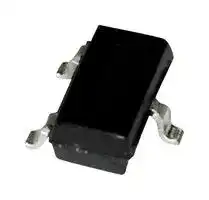


SST174-E3
JFET Transistor, JFET, 30 V, -135 mA, 10 V, TO-236, 3 Pin, 150 °C
- Manufacturer: VISHAY
- Product type: JFETs
- Breakdown Voltage Vbr:30V; Zero Gate Voltage Drain Current Idss Min:-20mA; Zero Gate Voltage Drain Current Idss Max:-135mA; Gate-Source Cutoff Voltage Vgs(off) Max:10V; Transistor Case Style:TO-236;
- SVHC: No SVHC (15-Jun-2015)
- Channel Type: P Channel
- Product Range: -
- Qualification: -
- Transistor Mounting: Surface Mount
- Operating Temperature Max: 150°C
- Gate Source Breakdown Voltage Max: 30V
- Zero Gate Voltage Drain Current Max: -135mA
| Delivery and price | |
|---|---|
| Units per pack | 7500 |
| Price | 0.267 € |
| Current stock | 10+ |
| Lead time | 30 days |
**J/SST174/175/176/177 Series**

## **Vishay Siliconix**

## **P-Channel JFETs**

**J174 SST174 J175 SST175 J176 SST176 J177 SST177**

|PRODUCT SUMMARY<br>~~es<2~~|PRODUCT SUMMARY<br>~~es<2~~|PRODUCT SUMMARY<br>~~es<2~~|PRODUCT SUMMARY<br>~~es<2~~|PRODUCT SUMMARY<br>~~es<2~~|
|---|---|---|---|---|
|**Part Number**<br>~~es~~|**VGS(off) (V)**<br>~~<2~~|**rDS(on) Max ( )**<br>~~<2~~|**ID(off) Typ (pA)**<br>~~<2~~|**tON  Typ (ns)**<br>~~<2~~|
|J/SST174<br>~~es~~<br>~~ee~~|5 to 10<br>~~<2~~|85<br>~~<2~~|–10<br>~~<2~~|25<br>~~<2~~|
|J/SST175<br>~~ee~~<br>~~es~~|3 to 6|125|–10|25|
|J/SST176<br>~~ee~~<br>~~es~~|1 to 4|250|–10|25|
|J/SST177<br>~~es~~|0.8 to 2.25|300|–10|25|


Analog Switches Choppers Sample-and-Hold Normally “On” Switches Current Limiters

e Low On-Resistance:  J174 <85 Qe Low Error Voltage Analog Switches e Fast Switching—tON:  25 ns e High-Speed Analog Circuit Performance e Choppers e Low Leakage: –10 pA e Negligible “Off-Error,” Excellent Accuracy Sample-and-Hold e Low Capacitance:  5 pF e Good Frequency Response e Normally “On” Switches e Low Insertion Loss e Eliminates Additional Buffering e Current Limiters

The J/SST174 series consists of p-channel analog switches designed to provide low on-resistance and fast switching.  This series simplifies series-shunt switching applications when combined with the Siliconix J/SST111 series.

The TO-226AA (TO-92) plastic package provides a low-cost option, while the TO-236 (SOT-23) package provides surface-mount capability.  Both the J and SST series are available in tape-and-reel for automated assembly (see Packaging Information).

**==> picture [327 x 168] intentionally omitted <==**

**----- Start of picture text -----**<br>
TO-226AA<br>(TO-92) TO-236<br>(SOT-23)<br>D 1<br>D 1<br>3 G<br>G 2<br>S 2<br>S<br>3<br>Top View<br>Top View<br>SST174 (S4)*<br>J174 SST175 (S5)*<br>J175 SST176 (S6)*<br>J176 SST177 (S7)*<br>J177<br>**----- End of picture text -----**<br>


*Marking Code for TO-236

For applications information see AN104.

Document Number:  70257 S-04030—Rev. E, 04-Jun-01

www.vishay.com

**9-1**

## **J/SST174/175/176/177 Series** ~~CSS~~ HAY **Vishay Siliconix**

Gate-Drain Voltage . . . . . . . . . . . . . . . . . . . . . . . . . . . . . . . . . . . . . . . . . . . . . 30 V Lead Temperature ([1] /16” from case for 10 sec.) . . . . . . . . . . . . . . . . . . . 300 C Gate-Source Voltage . . . . . . . . . . . . . . . . . . . . . . . . . . . . . . . . . . . . . . . . . . . . 30 V Power Dissipation[a] . . . . . . . . . . . . . . . . . . . . . . . . . . . . . . . . . . . . . . . . . 350 mW Gate Current . . . . . . . . . . . . . . . . . . . . . . . . . . . . . . . . . . . . . . . . . . . . . . . . –50 mA Storage Temperature . . . . . . . . . . . . . . . . . . . . . . . . . . . . . . . . . . . –55 to 150 C Notes Operating Junction Temperature . . . . . . . . . . . . . . . . . . . . . . . . . . –55 to 150 C a. Derate 2.8 mW/ C above 25 C

|~~Pp~~|~~Pp~~|~~Pp~~|~~Pp~~|~~Pp~~|~~Pp~~|~~Pp~~|~~Pp~~|~~Pp~~|~~Pp~~|
|---|---|---|---|---|---|---|---|---|---|
|**Parameter**<br>~~a~~|**Symbol**<br>~~a~~|**Test Conditions**<br>~~a~~||**Typa**<br>~~Pp~~<br>~~a~~<br>~~|~~|**Limits**<br>~~Pp~~<br>~~a~~||||**Unit**|
||||||J/SST174<br>~~Pp~~<br>~~a~~<br>~~|ot~~<br>~~|~~||J/SST175<br>~~a~~|||
||||||**Min**<br>~~a~~<br>~~|ot~~|**Max**<br>~~a~~<br>~~ot~~<br>~~|~~|**Min**<br>~~a~~|**Max**<br>~~a~~||
|**Static**<br>~~| ot~~<br>~~|~~<br>~~|~~<br>~~————oeeeeae~~||||||||||
|Gate-Source Breakdown Voltage<br>~~————~~|V(BR)GSS<br>~~————~~|IG= 1 A , VDS= 0 V<br>~~————~~||45<br>~~oe~~|30<br>~~oe~~|~~eee~~|30<br>~~eee~~|~~eee~~|V<br>~~ae~~|
|Gate-Source Cutoff Voltage<br>~~————~~<br>~~a~~|VGS(off)<br>~~————~~<br>~~eG~~|VDS= –15 V, ID= –10 nA<br>~~————~~<br>~~eG~~||~~oe~~<br>~~eG~~|5<br>~~oe~~<br>~~eG~~<br>~~GO~~|10<br>~~eee~~<br>~~eG~~<br>~~GO~~|3<br>~~eee~~<br>~~eG~~<br>~~OO~~|6<br>~~eee~~<br>~~eG~~<br>~~OO~~||
|Saturation Drain Currentb<br>~~————~~<br>~~a~~|IDSS<br>~~————~~<br>~~OG~~|VDS= –15 V, VGS= 0 V<br>~~————~~<br>~~OG~~||~~oe~~<br>~~OG~~|–20<br>~~oe ~~<br>~~OG~~<br>~~GO~~|–135<br> ~~eee~~<br>~~OG~~<br>~~GO~~|–7<br>~~eee~~<br>~~OG~~<br>~~OO~~|–70<br>~~eee ~~<br>~~OG~~<br>~~OO~~|mA<br> ~~ae~~<br>~~OG~~|
|Gate Reverse Current<br>~~ee~~<br>~~a~~|IGSS<br>~~ee~~<br>~~G~~|VGS= 20 V, VDS= 0 V<br>TA= 125 C<br>~~ee~~<br>~~es~~<br>~~GG~~||0.01<br>~~ee~~<br>~~ee~~|~~GO~~<br>~~ee~~<br>~~ee~~|1<br>~~GO ~~<br>~~ee~~<br>~~ee~~|~~OO~~<br>~~ee~~<br>~~ee~~|1<br>~~OO~~<br>~~ee~~<br>~~ee~~|nA<br>~~ee~~|
||||TA= 125 C<br>~~ee~~<br>~~es~~<br>~~G~~|5<br>~~ee~~<br>~~es~~<br>~~ee~~<br>~~GO~~|~~ee~~<br>~~es~~<br>~~ee~~<br>~~GO~~|~~ee~~<br>~~es~~<br>~~ee~~<br>~~OO~~|~~ee~~<br>~~es~~<br>~~ee~~|~~ee~~<br>~~es~~<br>~~ee~~||
|Gate Operating Current<br>~~a~~|IG<br>~~G~~|VDG= –15 V, ID= –1 mA<br>~~GG~~||0.01<br>~~ee ~~<br>~~GO~~|~~ee~~<br>~~GO~~|~~ee ~~<br>~~OO~~|~~ee ~~|~~ee~~||
|Drain Cutoff Current<br>~~a~~|ID(off)<br>~~G~~|VDS= –15 V, VGS= 10 V<br>TA= 125 C<br>~~GG~~<br>~~ee~~||–0.01<br>~~GO~~<br>~~ee~~|~~GO ~~<br>~~ee~~|–1<br> ~~OO~~<br>~~ee~~|~~ee~~|–1<br>~~ee~~||
||||TA= 125 C<br>~~ee~~|–5<br>~~ee~~|~~ee~~|~~ee~~<br>~~QO~~|~~ee~~<br>~~QO~~|~~ee~~||
|Drain-Source On-Resistance<br>~~a~~|rDS(on)<br>~~GG~~|VGS= 0 V, VDS= –0.1 V<br>~~ee ~~<br>~~GG~~||~~ee~~<br>~~GG~~|~~ee~~<br>~~GG~~|85<br>~~ee ~~<br>~~GG~~<br>~~QO~~|~~ee ~~<br>~~GG~~<br>~~QO~~|125<br> ~~ee~~<br>~~GG~~|~~ee~~<br>~~GG~~|
|Gate-Source Forward Voltage<br>~~pO~~|VGS(F)<br>~~pO~~|IG= –1 mA , VDS= 0 V<br>~~pO~~||–0.7<br>~~pO~~|~~pO~~|~~QO~~<br>~~pO~~|~~QO~~<br>~~pO~~|~~pO~~|V<br>~~pO~~|
|**Dynamic**<br>~~|~~<br>~~eeee a~~<br>~~ee~~||||||||||
|Common-Source<br>Forward Transconductance<br>~~ee~~|gfs<br>~~ee a~~|**VDS = –15 V, ID = –1 mA**<br>f = 1 kHz<br>~~a~~||4.5<br>~~ee~~|~~ee~~||||mS|
|Common-Source<br>Output Conductance<br>~~ee~~<br>~~a~~|gos<br>~~ee a~~<br>~~a~~|||20<br>~~ee~~|~~ee~~<br>~~Oe~~|~~GO~~|~~QO~~|~~QO~~|S|
|Drain-Source On-Resistance<br>~~ee ~~<br>~~a ~~<br>~~a~~|rds(on)<br> ~~ee a~~<br> ~~GG~~<br>~~a~~|VGS= 0 V, ID= 0 mA , f = 1 kHz<br>~~a~~<br>~~GG~~||~~ee~~<br>~~GG~~|~~ee~~<br>~~GG~~<br>~~Oe~~|85<br>~~GG~~<br>~~GO~~|~~GG~~<br>~~QO~~|125<br>~~GG~~<br>~~QO~~|~~GG~~|
|Common-Source Input Capacitance<br>~~a~~|Ciss<br>~~a~~|VDS= 0 V, VGS= 0 V, f = 1 MHz||20|~~Oe~~|~~GO ~~|~~QO~~|~~QO~~|pF|
|Common-Source<br>Reverse Transfer Capacitance|Crss|VDS= 0 V, VGS= 10 V<br>f = 1 MHz||5||||||
|Equivalent Input Noise Voltage|e<br>n|VDG= –10 V, ID= –1 mA<br>f = 1 kHz||20|||||nV⁄<br>~~√~~Hz|
|**Switching**<br>~~pe~~<br>~~Po~~<br>~~**e**e~~<br>~~eeee~~||||||||||
|Turn-On Time<br>~~Po~~<br>~~|~~<br>~~Po~~<br>~~|~~|td(on)<br>~~|~~|V**GS(L)**= 0 V, V**GS(H)**= 10 V<br>See Switching Circuit||10<br>~~**e**e~~|~~e~~|~~ee~~<br>~~e~~|~~ee~~<br>~~e~~<br>~~ee~~|~~ee~~<br>~~e~~<br>~~ee~~|ns<br>~~ee~~|
||tr<br>~~|~~<br>~~|~~|||15<br>~~**e**e~~<br>~~re~~|~~e~~<br>~~e~~~~**e**~~|~~ee~~<br>~~e~~<br>~~**ee**~~|~~ee~~<br>~~e~~<br>~~ee~~<br>~~**ee**~~|~~ee~~<br>~~e~~<br>~~ee~~<br>~~**ee**~~||
|Turn-Off Time<br>~~Po~~<br>~~|~~<br>~~Po~~<br>~~|~~|td(off)<br>~~|~~<br>~~|~~|||10<br>~~**e**e~~<br>~~re~~<br>~~a~~|~~e~~<br>~~e~~~~**e**~~<br>~~e~~|~~ee~~<br>~~e~~<br>~~**ee**~~|~~ee ~~<br>~~e~~<br>~~ee~~<br>~~**ee**~~|~~ee~~<br>~~e~~<br>~~ee~~<br>~~**ee**~~||
||tf<br>~~|~~|||20<br>~~re~~<br>~~a~~|~~e~~~~**e**~~<br>~~e~~|~~**ee**~~|~~ee~~<br>~~**ee**~~|~~ee~~<br>~~**ee**~~||


Notes a. Typical values are for DESIGN AID ONLY, not guaranteed nor subject to production testing. b. Pulse test:  PW < 300 s duty cycle uw < 3%.

Document Number:  70257 S-04030—Rev. E, 04-Jun-01

www.vishay.com **9-2**

**J/SST174/175/176/177 Series** ~~a~~ **Vishay Siliconix**

|||||||||||
|---|---|---|---|---|---|---|---|---|---|
|**Parameter**<br>~~a~~|**Symbol**|**Test Conditions**||**Typa**<br>~~|~~|**Limits**<br>~~po~~||||**Unit**|
||||||J/SST176<br>~~po~~<br>~~||~~<br>~~**|**~~||J/SST177<br>~~po~~|||
||||||**Min**<br>~~po~~<br>~~||~~|**Max**<br>~~po~~<br>~~**|**~~|**Min**<br>~~po~~|**Max**<br>~~po~~||
|**Static**<br>~~| |~~<br>~~**|**~~<br>~~es~~||||||||||
|Gate-Source Breakdown Voltage<br>~~———~~|V(BR)GSS<br>~~———~~|IG= 1 A , VDS= 0 V<br>~~———~~||45<br>~~ee~~|30<br>~~ee~~<br>~~GO~~|~~ee~~|30<br>~~ee~~|~~ee~~|V<br>~~ee~~|
|Gate-Source Cutoff Voltage<br>~~———~~<br>~~GO~~|VGS(off)<br>~~———~~<br>~~GO~~|VDS= –15 V, ID= –10 nA<br>~~———~~<br>~~GO~~||~~ee~~<br>~~GO~~<br>~~GG~~|1<br>~~ee~~<br>~~GO~~<br>~~GO~~<br>~~GG~~|4<br>~~ee~~<br>~~GO~~<br>~~GG~~|0.8<br>~~ee~~<br>~~GO~~<br>~~OO~~|2.25<br>~~ee~~<br>~~GO~~<br>~~OO~~||
|Saturation Drain Currentb<br>~~GG~~|IDSS<br>~~GG~~|VDS= –15 V, VGS= 0 V<br>~~GG~~||~~GG~~<br>~~GG~~|–2<br>~~GO~~<br>~~GG~~<br>~~GG~~|–35<br>~~GG~~<br>~~GG~~|–1.5<br>~~GG~~<br>~~OO~~|–20<br>~~GG~~<br>~~OO~~|mA<br>~~GG~~|
|Gate Reverse Current<br>~~Oe~~|IGSS<br>~~Oe~~|VGS= 20 V, VDS= 0 V<br>TA= 125 C<br>~~Oe~~<br>~~es~~||0.01<br>~~GG~~<br>~~Oe~~|~~GG~~<br>~~Oe~~|1<br>~~GG~~<br>~~Oe~~|~~OO~~<br>~~Oe~~|1<br>~~OO~~<br>~~Oe~~|nA|
||||TA= 125 C<br>~~Oe~~<br>~~es~~|5<br>~~Oe~~<br>~~es~~|~~Oe~~<br>~~es~~<br>~~GO~~|~~Oe~~<br>~~es~~<br>~~GO~~|~~Oe~~<br>~~es~~<br>~~GO~~|~~Oe~~<br>~~es~~||
|Gate Operating Current<br>~~a~~|IG<br>~~GG~~<br>~~ee~~|VDG= –15 V, ID= –1 mA<br>~~GG~~<br>~~eeee~~||0.01<br>~~GG~~<br>~~ee~~|~~GG~~<br>~~GO~~<br>~~ee~~|~~GG~~<br>~~GO~~<br>~~ee~~|~~GG~~<br>~~GO~~<br>~~ee~~|~~GG~~<br>~~ee~~||
|Drain Cutoff Current<br>~~ee~~|ID(off)<br>~~ee~~<br>~~ee~~|VDS= –15 V, VGS= 10 V<br>TA= 125 C<br>~~ee~~<br>~~eeee~~||–0.01<br>~~ee~~<br>~~ee~~<br>~~ee~~|~~GO~~<br>~~ee~~<br>~~ee~~<br>~~ee~~|–1<br>~~GO~~<br>~~ee~~<br>~~ee~~<br>~~ee~~|~~GO~~<br>~~ee~~<br>~~ee~~<br>~~ee~~|–1<br>~~ee~~<br>~~ee~~||
||||TA= 125 C<br>~~ee~~<br>~~ee~~|–5<br>~~ee~~<br>~~ee~~<br>~~ee~~|~~ee~~<br>~~ee~~<br>~~ee~~|~~ee~~<br>~~ee~~<br>~~ee~~|~~ee~~<br>~~ee~~<br>~~ee~~|~~ee~~<br>~~ee~~||
|Drain-Source On-Resistance<br>~~po~~<br>~~pO~~|rDS(on)<br>~~ee~~<br>~~po~~|VGS= 0 V, VDS= –0.1 V<br>~~eeee~~<br>~~po~~||~~ee~~<br>~~ee~~<br>~~po~~|~~ee~~<br>~~ee~~<br>~~po~~|250<br>~~ee~~<br>~~ee~~<br>~~po~~|~~ee~~<br>~~ee~~<br>~~po~~|300<br>~~ee~~<br>~~po~~|~~po~~|
|Gate-Source Forward Voltage<br>~~pO~~|VGS(F)|IG= –1 mA , VDS= 0 V||–0.7|||||V|
|**Dynamic**<br>~~pO~~<br>~~a~~||||||||||
|Common-Source<br>Forward Transconductance<br>~~ff~~|gfs<br>~~ff~~|VDS= –15 V, ID= –1 mA<br>f = 1 kHz<br>~~ET~~||4.5<br>~~ET~~|~~ET~~|~~ET~~|~~ET~~||mS|
|Common-Source Output Conductance<br>~~ff~~|gos<br>~~ff~~|||20<br>~~ET~~|~~ET~~|~~ET~~|~~ET~~||S|
|Drain-Source On-Resistance<br>~~po~~|rds(on)<br>~~po~~|VGS= 0 V, ID= 0 mA , f = 1 kHz<br>~~po~~||~~po~~|~~po~~|250<br>~~po~~|~~po~~|300<br>~~po~~|~~po~~|
|Common-Source Input Capacitance<br>~~a~~|Ciss<br>~~a~~|VDS= 0 V, VGS= 0 V, f = 1 MHz<br>~~a~~||20<br>~~a~~|~~a~~|~~a~~|~~a~~|~~a~~|pF<br>~~a~~|
|Common-Source<br>Reverse Transfer Capacitance|Crss|VDS= 0 V, VGS= 10 V<br>f = 1 MHz||5||||||
|Equivalent Input Noise Voltage|e<br>n|VDG= –10 V, ID= –1 mA<br>f = 1 kHz||20|||||nV⁄<br>~~√~~Hz|
|**Switching**<br>~~a~~<br>~~pf~~<br>~~pf~~||||||||||
|Turn-On Time<br>~~pf~~<br>~~|~~<br>~~po~~<br>~~|~~|td(on)<br>~~pf~~<br>~~|~~|V**GS(L)**= 0 V, V**GS(H)**= 10 V<br>See Switching Circuit||10<br>~~pf~~<br>~~re~~|~~pf~~<br>~~ee~~|~~ee~~|||ns<br>~~**ee**~~|
||tr<br>~~pf~~<br>~~|~~<br>~~|~~|||15<br>~~pf~~<br>~~re~~<br>~~**ee**~~|~~pf~~<br>~~ee~~<br>~~ee~~|~~ee~~<br>~~ee~~|~~**ee**~~|~~**ee**~~||
|Turn-Off Time<br>~~|~~<br>~~po~~<br>~~|~~|td(off)<br>~~|~~<br>~~|~~|||10<br>~~re~~<br>~~**ee**~~|~~ee~~<br>~~ee~~<br>~~ee~~|~~ee~~<br>~~ee~~<br>~~ee~~|~~**ee**~~|~~**ee**~~||
||tf<br>~~|~~<br>~~|~~|||20<br>~~re~~<br>~~**ee**~~|~~ee~~<br>~~ee~~<br>~~ee~~|~~ee~~<br>~~ee~~<br>~~ee~~|~~**ee**~~|~~**ee**~~||


PSCIA

Document Number:  70257 S-04030—Rev. E, 04-Jun-01

www.vishay.com

**9-3**

**J/SST174/175/176/177 Series**

## **Vishay Siliconix**

**==> picture [233 x 618] intentionally omitted <==**

**----- Start of picture text -----**<br>
On-Resistance and Drain Current<br>vs. Gate-Source Cutoff Voltage<br>200 –100<br>IDSS<br>160 ||CCEELEE, tt | ty ZEa –80<br>PINT | | | tA<br>rDS<br>120 –60<br>A EA<br>Pi KET {TA lf<br>80 –40<br>PT| ITNT YE | tt<br>| | pA |<br>40 — –20<br>rDS @ ID = –1 mA, VGS = 0 V<br>iY IDSS @ VDS = –15 V, VGS = 0 V<br>| |<br>0 mid 0<br>0 2 4 6 8 10<br>VGS(off) – Gate-Source Cutoff Voltage (V)<br>Output Characteristics<br>–25<br>|| VGS(off) = 3 V | | | VGS = 0 V<br>So eee<br>–20 lA TTT |<br>0.5 V<br>–15<br>fi titi<br>f[ATTTETT |<br>1.0 V<br>–10 df | | |<br>1.5 V<br>fae<br>–5 A<br>2.0 V<br>| Se e<br>0 Zn<br>0 –4 –8 –12 –16 –20<br>VDS – Drain-Source Voltage (V)<br>Output Characteristics<br>–2<br>VGS = 0 V<br>1.5 V<br>–1.6 0.5 V [77Via ane<br>1.0 V [fA Z7<br>||<br>V//\|<br>–1.2<br>7 | | | |<br>2.0 V<br>HES ba<br>–0.8<br>WZ<br>Yi 7 a<br>–0.4 POZO Ee<br>0 aa{[““—s VGS(off) = 3 V<br>0 –0.1 –0.2 –0.3 –0.4 –0.5<br>VDS – Drain-Source Voltage (V)<br>Ω ) I<br> – Drain-Source On-Resistance (  DSS<br> – Saturation Drain Current (mA)<br>rDS(on)<br>– Drain Current (mA)<br>I D<br>– Drain Current (mA)<br>I D<br>**----- End of picture text -----**<br>


**==> picture [227 x 619] intentionally omitted <==**

**----- Start of picture text -----**<br>
Forward Transconductance and Output Conductance<br>vs. Gate-Source Cutoff Voltage<br>18 250<br>gfs and gos @ VDS = –15 V<br>VGS = 0 V, f = 1 kHz<br>a<br>15 pat| 200<br>ei lATA]|<br>gfs<br>12 nye aneee 150<br>gos<br>a4, 40a<br>9 A7lLyi | tit 100<br>fi7At<br>6 AA 50<br>ty<br>FF) | | i || | Etttt .<br>3 eT [EET] ET | tt 0<br>0 2 4 6 8 10<br>VGS(off) – Gate-Source Cutoff Voltage (V)<br>On-Resistance vs. Drain Current<br>250<br>200 CE TA = 25 C 0llRI<br>VGS(off) = 1.5 V<br>Po A TT<br>150<br>74 |<br>eT IOA<br>3 V<br>100<br>eee Ae ill<br>5 V<br>a.<br>50 A | et|<br>0 oon ooo<br>–1 –10 –100<br>ID – Drain Current (mA)<br>On-Resistance vs. Temperature<br>300<br>ID = –1 mA<br>rDS changes X 0.7%/ C<br>240<br>Py SER<br>Tie<br>{| | | | |Lb<br>180<br>VGS(off) = 1.5 V<br>a aaa<br>3 V<br>120 | | ao | | ld<br>5 V<br>AE<br>E T<br>60 S== nee<br>0 SEPPeeeerrr<br>–55 –35 –15 5 25 45 65 85 105 125<br>TA – Temperature ( C)<br>gos<br>– Output Conductance (<br> – Forward Transconductance (mS) S)<br>fs<br>g<br>Ω )<br> – Drain-Source On-Resistance (<br>rDS(on)<br>Ω )<br> – Drain-Source On-Resistance (<br>rDS(on)<br>**----- End of picture text -----**<br>


Document Number:  70257 S-04030—Rev. E, 04-Jun-01

www.vishay.com

**9-4**

**J/SST174/175/176/177 Series** ~~a~~ **Vishay Siliconix**

**==> picture [484 x 615] intentionally omitted <==**

**----- Start of picture text -----**<br>
Turn-On Switching Turn-Off Switching<br>50 20<br>tr approximately independent of ID<br>VVDDGS(H) = –10 V, R = 10 V, VGGS(L) = 220  = 0 V tf VGS(off) = 1.5 V<br>40 Fo 16 E AE<br>5 V<br>FCRCCEECEEnN S Y IN EE<br>30 tON @ ID = –5 mA tON @ ID = –10 mA 12<br>SST PEE td(off) VGS(off) = 1.5 V PS<br>SANE eo SEE<br>20 8<br>5 V<br>ARK KE AR K ER<br>10 TE NINONSNISS_| IN 4 COL OORTee<br>tr @ ID = –5 mA<br>0 COTTE Se 0 VDD = –10 V, VGS(H) = 10 V, VGS(L) = 0 V<br>0 Foree 1 2 eepe 3 4 5 = Ei 0 –3 –6 –9 –12 –15<br>VGS(off) – Gate-Source Cutoff Voltage (V) ID – Drain Current (mA)<br>Capacitance vs. Gate-Source Voltage Gate Leakage Current<br>30 100 nA<br>VDS = 0 V TT ID = –1 mA<br>f = 1 MHz 10 nA<br>24 Eo LLL –10 mA<br>A CeEEEEE PL TA = 125 C<br>1 nA<br>18 VCLLELLELL ei Law<br>IGSS @ 125 C<br>Ciss 100 pA<br>12 PE CINCEEP ey TT T –10 mA MA<br>Crss  ELLE 10 pA TA = 25 C East<br>O SE S oe<br>6 S a == 1 pA et –1 mA I A GSS @ 25 C<br>ee fo<br>0 FEEL 0.1 pA ‘ ARE<br>0 4 8 12 16 20 0 –10 –20 –30 –40 –50<br>VGS – Gate-Source Voltage (V) VDG – Drain-Gate Voltage (V)<br>Transfer Characteristics Noise Voltage vs. Frequency<br>–40 100<br>VGS(off) = 3 V VDS = –15 V<br>–32 ID = –0.1 mA<br>PT  PTT TT a TSRS RC SH<br>–24 TA = –55 C –1 mA<br>Ce Oooo e |||eg 10 a assssaeRE TNOamS|<br>25 C<br>–16–8 LANINNA P| tf| || ft| ft| fl[i A a ee atll<br>VDS = –10 V<br>0 o 125 C NeNLET | 1 SHONTLEart ati<br>0 1 2 3 4 5 10 100 1 k 10 k 100 k<br>VGS – Gate-Source Voltage (V) f – Frequency (Hz)<br>Switching Time (ns) Switching Time (ns)<br>– Gate Leakage<br>Capacitance (pF)<br>I G<br>– Drain Current (mA)<br>I D<br>n – Noise Voltage  nV /    Hz<br>e<br>**----- End of picture text -----**<br>


Document Number:  70257 S-04030—Rev. E, 04-Jun-01

www.vishay.com

**9-5**

## **J/SST174/175/176/177 Series** ~~SNS~~ **Vishay Siliconix**

||||||
|---|---|---|---|---|
|~~es~~|**174**<br>~~ee~~|**175**<br>~~ee~~|**176**|**177**|
|VDD<br>~~es~~|–10 V<br>~~ee~~|–6 V<br>~~ee~~|–6 V|–6 V|
|VGG<br>~~es~~|20 V<br>~~ee~~|12 V<br>~~ee~~|8 V|5 V|
|RL*|560|750|1800|5600|
|RG*<br>~~a~~|100|220|390|390|
|ID(on)<br>~~a~~|–15 mA|–7 mA|–3 mA|–1 mA|


Rise Time < 1 ns Rise Time 0.4 ns Fall Time < 1 ns Input Resistance 10 M Q Pulse Width 100 ns Input Capacitance 1.5 pF PRF 1 MHz

**==> picture [188 x 160] intentionally omitted <==**

**----- Start of picture text -----**<br>
VGG VDD<br>1.2 k RL<br>VGS(H) °<br>VGS(L) 0.1 F<br>RG<br>7.5 k<br>51  Q 1.2 k Q 7<br>Sampling<br>Scope<br>51  51<br>**----- End of picture text -----**<br>


See Typical Characteristics curves for changes.

Document Number:  70257 S-04030—Rev. E, 04-Jun-01

www.vishay.com **9-6**

**Legal Disclaimer Notice**

Vishay

**==> picture [60 x 50] intentionally omitted <==**

## **Notice**

Specifications of the products displayed herein are subject to change without notice. Vishay Intertechnology, Inc., or anyone on its behalf, assumes no responsibility or liability for any errors or inaccuracies.

Information contained herein is intended to provide a product description only. No license, express or implied, by estoppel or otherwise, to any intellectual property rights is granted by this document. Except as provided in Vishay's terms and conditions of sale for such products, Vishay assumes no liability whatsoever, and disclaims any express or implied warranty, relating to sale and/or use of Vishay products including liability or warranties relating to fitness for a particular purpose, merchantability, or infringement of any patent, copyright, or other intellectual property right.

The products shown herein are not designed for use in medical, life-saving, or life-sustaining applications. Customers using or selling these products for use in such applications do so at their own risk and agree to fully indemnify Vishay for any damages resulting from such improper use or sale.

Document Number: 91000 Revision: 08-Apr-05

www.vishay.com 1
Updated at April 1, 2026
Vishay is a global leader in the manufacturing of discrete semiconductors and passive electronic components. Renowned for its exceptional quality and engineering expertise, the company produces highly reliable solutions that drive innovation across the industrial, automotive, telecommunications, and consumer electronics markets. From advanced factory automation to vehicle electrification, Vishay components provide the foundational building blocks for modern electronic design. The company's expansive portfolio is heavily focused on efficient power management, signal routing, and energy storage. Within its passive component lineup, Vishay is recognized for its extensive array of high-performance capacitors, including robust aluminium electrolytic, film, and polymer variants, alongside highly efficient power inductors. In the realm of discrete semiconductors, Vishay is a premier manufacturer of single and dual MOSFETs, as well as a vast selection of Schottky, Zener, and fast-recovery rectifier diodes designed for demanding power applications. Furthermore, Vishay delivers industry-leading circuit protection and thermal management solutions. With a broad offering of transient voltage suppressors (TVS diodes) and temperature-sensing NTC thermistors, these components are engineered to safeguard sensitive circuitry against both electrical and thermal overstress. By combining this vital mix of advanced discretes and passives, Vishay enables engineers to develop robust, space-saving, and highly resilient electronic systems.
About Novapart
Novapart is a B2B electronic component broker specialising in stock shortages and cost reduction. We source hard-to-find parts and identify compliant alternatives across a catalogue of 540,000+ components from 500+ manufacturers.
Learn more →Stock Shortage Specialist
When a component is unavailable, discontinued or has an unacceptable lead time, we tap into our network of vetted European and Asian distributors to source what you need — without compromising on quality or traceability.
Request a quote →Compliant Alternatives
We identify pin-to-pin, electrically equivalent substitutes that meet the same certifications (RoHS, AEC-Q100, REACH) as your original specification — validated against datasheets, not just part numbers. Often at a lower cost.
BOM Analysis service →