
Image not available
Illustrative purposes only

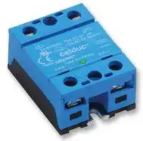
SOM040100
MOSFET Relay, 60 VDC, 40 A, 0.03 ohm
⚠️ Reference pricing provided. In case of supply shortages, we will connect you with our trusted procurement partners to ensure your project's continuity.
- Manufacturer: CELDUC
- Product type: MOSFET Solid State Relays
- Contact Configuration:-; Load Current:40A; Relay Terminals:Screw; Load Voltage Max:60VDC; On State Resistance Max:0.03ohm; Isolation Voltage:2.5kV; Forward Current If:35mA; Product Range:-; SVH
- SVHC: No SVHC (27-Jun-2024)
- Load Type: DC
- Contact Form: -
- Load Current: 40A
- Product Range: okpac SOM Series
- Relay Mounting: Panel Mount
- Relay Terminals: Screw
- Load Voltage Max: 60V
- Isolation Voltage: 2.5kV
- Forward Current If: 35mA
- I/O Capacitance Typ: -
- On State Resistance Max: 0.03ohm
- MOSFET Relay Package Style: Hockey Puck
- Off State Leakage Current Max: -
| Delivery and price | |
|---|---|
| Units per pack | 10 |
| Price | 99.09 € |
| Current stock | 10+ |
| Lead time | 30 days |
Datasheet

**S/CON/SOM040100/B/18/12/14** **Page 1/5 UK** ## MOSFET BASED DC SOLID-STATE RELAY ## SOM040100 - Latest MOSFET technology generation. - Ultra low on-state resistance. - Low output leakage current. - Low control current consumption. - Built-in overvoltage protection - Reverse protected triggered control input to avoid linear control risks **==> picture [508 x 357] intentionally omitted <==** **----- Start of picture text -----**<br> Control voltage range 3.5-32VDC<br>No radiated or conducted disturbances<br>Max. permanent<br>60VDC<br>Touch protected housing IP20 output voltage<br>Max. load current<br>40ADC<br>with heatsink<br>Control input In & case / Out Dimensions<br>Load voltage range Load current range voltage range Insulation Connections (WxHxD) Weight<br>5-60VDC (with heatsink)Up to 40A 3.5-32VDC 2.5kV Screw terminals 45 x 58.5 x 30 80g<br>HIGH SIDE WIRING DIAGRAM LOW SIDE WIRING DIAGRAM<br>Fig. 1 Fig. 2<br>(Load connected to “-“) (Load connected to “+”)<br>“OC. sono<br>_ bc + Pow er supply _ + _ pe +<br>I “I Ul II I Mains I See Instruction<br>See Instruction<br>sheet to select<br>Ue le sheet to select the Ue le<br>the right<br>C1 L. + Control right protective Ri od protective<br>components<br>x ae Oe : © | J Ci components<br>The red paths<br>po HOLL ‘ 9 (C1/D2) must be Ic 6 iF _8 D2 The red paths<br>(C1/D2) must<br>@ Is 4 @ as short as onicre | @D PE “}@<br>: Control . be as short as<br>possible !<br>possible !<br>iil TT<br>Fig. 3 INTERNAL DIAGRAM<br>**----- End of picture text -----**<br> - No radiated or conducted disturbances - Touch protected housing IP20 # **®** _Proud to serve you_ **celduc** ~~e~~ Data given at Tambient=25°C and subject to modification without previous notice **r e l a i s** **celduc® r e l a i s** **S/CON/SOM040100/C/18/12/14** **Page 2/5 UK** ||||CONTROL INPUT CHARACTERISTICS|CONTROL INPUT CHARACTERISTICS|CONTROL INPUT CHARACTERISTICS|CONTROL INPUT CHARACTERISTICS| |---|---|---|---|---|---|---| |||||||| |INPUT CIRCUIT|CHARACTERISTIC<br>Nom. Control voltage<br>Min. Control current<br>Control voltage range<br>Control current consumption<br>Releasingcontrol voltage<br>Max. reverse control voltage|LABEL<br>Ucnom<br>Icmin<br>Uc<br>Ic<br>Ucoffmax<br>-Ucmax|VALUE<br>12-24VDC<br>35mADC<br>3.5 – 32VDC<br>32 – 35mADC(for control voltage range)<br>1VDC<br>32VDC|||INFO.<br>-100µA/°C<br>typical ON=3.3V<br>See fig. 5<br>typical OFF= 2.6V<br>-Icmax<100µA| ||Input impedance|Rin|Current limitation|||See fig. 5| |||||||| ||||POWER OUTPUT CHARACTERISTICS|||| ||CONTROL INPUT CHARACTERISTICS|CONTROL INPUT CHARACTERISTICS|CONTROL INPUT CHARACTERISTICS|CONTROL INPUT CHARACTERISTICS|CONTROL INPUT CHARACTERISTICS|CONTROL INPUT CHARACTERISTICS| |---|---|---|---|---|---|---| |||||||| |IT|CHARACTERISTIC|LABEL||VALUE||INFO.| |U|Nom. Control voltage|Ucnom||12-24VDC||| |RC|Min. Control current|Icmin||35mADC||-100µA/°C| |CI|Control voltage range|Uc||3.5 – 32VDC||typical ON=3.3V| |T|Control current consumption|Ic||32 – 35mADC(for control voltage range)||See fig. 5| |PU|Releasingcontrol voltage|Ucoffmax||1VDC||typical OFF= 2.6V| |N|Max. reverse control voltage|-Ucmax||32VDC||-Icmax<100µA| |I|Input impedance|Rin||Current limitation||See fig. 5| |||||||| |||||POWER OUTPUT CHARACTERISTICS||| |||||||| |POWER CIRCUIT|CHARACTERISTIC|LABEL||VALUE||INFO.| ||Nominal voltage|Uenom||48VDC||| ||Voltage range|Ut|Ue|5-60VDC||| ||Non-repetitive peak voltage|Utp||100V||| ||Overvoltage protection|D1||Transient voltage suppressor<br>56V (1500W/1ms)||| ||Max reverse voltage drop (internal<br>diode at OFF state)|-Ut||1.3V||@Ie=80A<br>@Uc=0| ||Maximum nominal currents|Ie max||Resistive|Motor|See fig. 7<br>(limits)| |||||40A|Please contact us|| ||Non-repetitive peak overload<br>current|Id max||320A||See fig. 8| ||Min. load current|Iemin||5mA||| ||Max. leakage current|Ielk max||3mA||@Utmax @Tjmax| ||Max. on-state resistance|RDSon||30mOhms||@Iemax @Tjmax| ||Typ. output capacitance|Cout||0.7nF||| ||Junction/case thermal resistance<br>perpowerelement|Rthjc||0.9K/W||| ||Built-in heatsink thermal<br>resistance verticallymounted|Rthra||10K/W||@Tra=75°C| ||Heatsink thermal time constant|Tthra||10 minutes||@Tra=75°C| ||Control inputs/power outputs<br>insulationvoltage|Uimp||2.5kV||| ||Inputs/case insulation voltage|Uimp||2.5kV||| ||Outputs/case insulation voltage|Uimp||2.5kV||| ||Isolation resistance|Rio||1G||| ||Isolation capacitance|Cio||<8pF||| ||Maximumjunction temperature|Tjmax||175°C||| ||Storage ambient temperature|Tstg||-40->+100°C||| ||Operatingambient temperature|Tamb||-25->+90°C||See fig. 7| ||Max. case temperature|Tc||100°C||| ## PROTECTION CHARACTERISTICS Leakage current (Ielk) vs DC voltage (Ut) **Ielk / Ie 1 0,8 0,6 0,4 0,2 0 0 10 20 30 40 50 60 70 80 90 100 Ut (V) U t max U t p ( =U emax)** Ielk : Leakage current of the relay Ie : User load nominal current Utp : Relay max. non repetitive peak voltage Absolute limits Uto Utp 0.75 t max (Uto Ut max) Ie P ( protection ) 1W max (Uto Ut max) Ie t 1 T Utmax : Uto Utn = Ue : : Possible overvoltage above Utmax Max. nominal voltage of the relayUser DC power supply voltage t :T: Overvoltage duration Time between 2 overvoltage **celduc® r e l a i s** **S/CON/SOM040100/C/18/12/14** **Page 3/5 UK** ## TIME CHARACTERISTICS **==> picture [516 x 133] intentionally omitted <==** **----- Start of picture text -----**<br> Fig. 4 TIME DIAGRAMS<br>**----- End of picture text -----**<br> |Fig. 4|TIME DIAGRAMS|TIME DIAGRAMS|TIME DIAGRAMS|TIME DIAGRAMS|TIME DIAGRAMS|TIME DIAGRAMS|TIME DIAGRAMS|TIME DIAGRAMS|TIME DIAGRAMS|TIME DIAGRAMS|TIME DIAGRAMS| |---|---|---|---|---|---|---|---|---|---|---|---| ||||||||||||| ||||||||||||| ||||||||||||| ||||||||||||| ||||||||||||| ||||||||||||| ||||||||||||| |TIME CHARACT.|CHARACTERISTIC||||LABEL|VALUE|||||INFO.| ||Turn on time||||ton|20µs|||||| ||Turn on delay||||tdon|20µs|||||| ||Turn off time||||toff|20µs|||||| ||Turn off delay||||tdoff|20µs|||||| ||Max. On-Off frequency||||F(on-off)|>1000Hz (for high frequency, take 2 x Ie to calculate the<br>heatsink; the protections must be chosen carefully)|||||Refer to the<br>instruction sheet| ||||||||||||| ||GENERAL INFORMATION||||||||||| ||||||||||||| |CONNECT<br>IONS|Connections|||||Power|||Control||| ||Screwdriver advised|||||POZIDRIV2|||||| ||Min and max tightening torque|||||2 N.m|||1.2 N.m||| ||Insulated crimp terminals (round<br>tabs, eyelet type)|||||M5|||M4||| ||||||||||||| |MISC.|Display|||||Green LED<br>(indicates relayhas switched ON)|||||| ||Housing|||||UL94V0|||||| ||Mounting|||||2 screws (M4x12mm ; tightening = 1.2N.m)|||||See mounting<br>sheet| ||Noise level|||||None|||||| ||Weight|||||80g|||||| ||||||||||||| ||STANDARDS||||||||||| ||||||||||||| |GENERAL|Standards|||||IEC60947-1|||||| ||Protection level|||||IP20|||||| ||Protection against direct touch|||||Yes|||||| ||CE marking|||||Yes|||||| ||UL, cULUS|||||Yes|||||| ||||||||||||| |E.M.C.<br>IMMUNITY|TYPE OF TEST||||STANDARD|LEVEL|||||EFFECT| ||Fast transients bursts||||EN61000-4-4|4kV criterion B|||||| ||Electric chocks||||EN61000-4-5|1kV criterion B|||||| ||Voltage drop||||EN61000-4-11|-|||||| **celduc® r e l a i s** **S/CON/SOM040100/C/18/12/14** **Page 4/5 UK** ## CHARACTERISTIC CURVES **==> picture [516 x 699] intentionally omitted <==** **----- Start of picture text -----**<br> Fig. 5 INPUT CHARACTERISTIC Fig. 6 ON RESISTANCE VS JUNCTION TEMPERATURE<br>Ic (mADC)<br>RDSon<br>50 30<br>-35°C-35°C (mOhms)<br>45<br>25<br>40<br>25°C<br>35<br>20<br>30 100°C<br>25 15<br>20<br>10<br>15<br>10<br>5<br>5<br>0 0<br>0 2 4 6 8 10 12 14 16 18 20 22 24 26 28 30 32 -50 0 50 100 150<br>Junction Temperature (°C)<br>Uc (VDC)<br>Fig. 7 POWER DISSIPATED AND LOAD CURRENT LIMIT VS TEMPERATURE<br>Permanent current Please refer to the installation notice for precautions about Power dissipated<br>Ie (ARMS) mounting the device on a heatsink. (W)<br>45 60.8<br>1.2K/W 1.1K/W 0.9K/W 0.75K/W 0.55K/W 0.3K/W<br>40 48<br>35 36.8<br>30 27<br>25 18.8<br>20 12<br>15 6.75<br>10 3<br>5 0.75<br>10K/W 4K/W 2.2K/W 2.1K/W<br>0 0<br>0 10 20 30 40 50 60 70 80 90 100 110<br>Ambient temperature (°C)<br>10K/W = No Heatsink 4K/W = 150x150x3mm aluminium sheet 2.2K/W = WF262100 2.2K/W = WF151200<br>2.1K/W = WF210000 1.2K/W = WF121000 1.1K/W = WF131100 0.9K/W = WF115100<br>0.75K/W = WF070000 0.55K/W = WF050000 0.3K/W = WF031100<br>Fig. 8 PEAK OVERLOAD CURRENT vs. PULSE DURATION CHARACTERISTIC<br>Ie 360<br>(Apk) 320 Non-repetitive D=1% (Tc=100°C, Tjmax=175°C)<br>280 Repetitive D=5% (Tc=100°C, Tjmax=175°C)<br>240<br>Repetitive D=10% (Tc=100°C, Tjmax=175°C)<br>200<br>160 Repetitive D=20% (Tc=100°C, Tjmax=175°C)<br>120<br>80<br> t 1 <br>D % t 2 100 400 Repetitive D=50% (Tc=100°C, Tjmax=125°C)<br>0,1 1 10 100 1000<br>Pulse duration (ms)<br>**----- End of picture text -----**<br> **celduc® r e l a i s** **S/CON/SOM040100/C/18/12/14** **Page 5/5 UK** DIMENSIONS AND ACCESSORIES **==> picture [509 x 368] intentionally omitted <==** **----- Start of picture text -----**<br> Fig. 9 DIMENSIONS (mm)<br>a<br>NY] (SUIS)<br>20<br>30 MAX (M5 7647<br>4)faeOre<br>2 - 1 +<br>x<br><—<br>=<br>Ww<br>: [eee :<br>**----- End of picture text -----**<br> Fig. ACCESSORIES 10 ~~a~~ FASTON : Please contact us **celduc® www.celduc.com r e l a i s** ~~a~~ Qualité **5 Rue Ampère B.P. 30004 42290 SORBIERS - FRANCE E-Mail : celduc-relais@celduc.com Fax +33 (0) 4 77 53 85 51 Service Commercial France Tél. : +33 (0) 4 77 53 90 20 Sales Dept.For Europe Tel. : +33 (0) 4 77 53 90 21 Sales Dept. Asia : Tél. +33 (0) 4 77 53 90 19**
Updated at June 3, 2026
About Novapart
Novapart is a B2B electronic component broker specialising in stock shortages and cost reduction. We source hard-to-find parts and identify compliant alternatives across a catalogue of 410,000+ components from 500+ manufacturers.
Learn more →Stock Shortage Specialist
When a component is unavailable, discontinued or has an unacceptable lead time, we tap into our network of vetted European and Asian distributors to source what you need — without compromising on quality or traceability.
Request a quote →Compliant Alternatives
We identify pin-to-pin, electrically equivalent substitutes that meet the same certifications (RoHS, AEC-Q100, REACH) as your original specification — validated against datasheets, not just part numbers. Often at a lower cost.
BOM Analysis service →