
Image not available
Illustrative purposes only

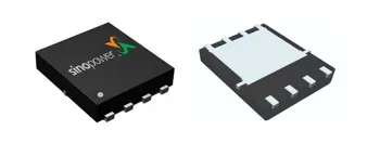
SM6128NSKP
SM6128NSKP, Single MOSFET, N Channel, 60V, DFN5x6A-8_EP1
⚠️ Reference pricing provided. In case of supply shortages, we will connect you with our trusted procurement partners to ensure your project's continuity.
- Manufacturer: Sinopower
- Product type: Single MOSFETs
- Cfg.: N
- BV(V): 60
- Package: View
- VGS (±V): 20
- VTH(V) typ.: 2
- ID (A) TA=25: 10
- ID (A) TC=25: 50
- Rg (Ω) typ.: 1
- Ciss (pF) typ.: 2500
- Coss (pF) typ.: 215
- Crss (pF) typ.: 105
- Tape & Reel: View
- Quality Report: View
- RON(mΩ max) 10V max.: 10.8
- RON(mΩ max) 4.5V max.: 13.5
| Delivery and price | |
|---|---|
| Units per pack | 1 |
| Price | Ask for quotation |
| Current stock | 10+ |
| Lead time | 30 days |
Datasheet

## **SM6128NSKP** **==> picture [4 x 4] intentionally omitted <==** **----- Start of picture text -----**<br> ®<br>**----- End of picture text -----**<br> N-Channel Enhancement Mode MOSFET ## **Features** **==> picture [125 x 14] intentionally omitted <==** **----- Start of picture text -----**<br> Pin Description<br>**----- End of picture text -----**<br> - 60V/50A, RDS(ON)=10.8mΩ (max.) @ VGS=10V - RDS(ON)=13.5mΩ (max.) @ VGS=4.5V - Reliable and Rugged - Lead Free and Green Devices Available - (RoHS Compliant) ## **Applications** - Secondary Side Synchronous Rectification - DC-DC Converter - Motor Control - Load Switching **==> picture [161 x 245] intentionally omitted <==** **----- Start of picture text -----**<br> [D] [D] |<br>D [D] |<br>[G] Pin 1<br>[S]<br>S [S]<br>DFN5x6-8<br>(5,6,7,8)<br>DD DD<br>(4) G |<br>S S S<br>( 1, 2, 3 )<br>**----- End of picture text -----**<br> N-Channel MOSFET ## **Ordering and Marking Information** **==> picture [470 x 202] intentionally omitted <==** **----- Start of picture text -----**<br> SM6128NS Package Code<br> KP : DFN5x6-8<br>Operating Junction Temperature Range<br>Assembly Material<br> C : -55 to 150 [o] C<br>Handling Code<br>Handling Code<br>Temperature Range<br> TR : Tape & Reel (2500ea/reel)<br>Package Code Assembly Material<br> G : Halogen and Lead Free Device<br>SM6128NS KP : SM6128 XXXXX - Lot Code<br>XXXXX<br>yo<br>j E |<br>Note : SINOPOWER lead-free products contain molding compounds/die attach materials and 100% matte tin plate<br>termination finish; which are fully compliant with RoHS. SINOPOWER lead-free products meet or exceed the lead-<br>free requirements of IPC/JEDEC J-STD-020D for MSL classification at lead-free peak reflow temperature. SINOPOWER<br>defines “Green” to mean lead-free (RoHS compliant) and halogen free (Br or Cl does not exceed 900ppm by weight<br>in homogeneous material and total of Br and Cl does not exceed 1500ppm by weight).<br>**----- End of picture text -----**<br> SINOPOWER reserves the right to make changes to improve reliability or manufacturability without notice, and advise customers to obtain the latest version of relevant information to verify before placing orders. _www.sinopowersemi.com_ 1 Copyright Sinopower Semiconductor, Inc. Rev. A.2 - January, 2014 **®** sinopower WN ## **SM6128NSKP** ## **Absolute Maximum Ratings** (TA = 25°C Unless Otherwise Noted) |**Symbol**<br>~~a ee~~|**Parameter**<br>~~ee~~|**Parameter**<br>~~ee~~|**Rating**<br>~~ee~~|**Unit**<br>~~ee~~| |---|---|---|---|---| |**Common Ratings **<br>~~|~~||||| |VDSS<br>~~**a**~~|Drain-Source Voltage<br>~~**a**~~||60<br>~~**a**~~|V<br>~~**a**~~| |VGSS<br>~~**a**~~|Gate-Source Voltage<br>~~**a**~~<br>~~ee~~||±20<br>~~**a**~~<br>~~ee~~|| |TJ<br>~~**a**~~<br>~~ee~~<br>~~es~~|Maximum Junction Temperature<br>~~**a**~~<br>~~ee~~<br>~~ee~~<br>~~ee~~||150<br>~~**a**~~<br>~~ee~~<br>~~ee~~<br>~~ee~~|°C<br>~~**a**~~<br>~~ee~~| |TSTG<br>~~ee~~<br>~~es~~|Storage Temperature Range<br>~~ee~~<br>~~ee~~<br>~~ee~~||-55 to 150<br>~~ee~~<br>~~ee~~|| |IS<br>~~es~~<br>~~a es~~|Diode Continuous Forward Current<br>~~ee~~<br>~~es~~|TC=25°C<br>~~ee~~<br>~~es~~<br>~~ee~~|25<br>~~ee~~<br>~~es~~|A<br>| |ID<br>~~a~~<br>~~a~~|Continuous Drain Current<br>~~a~~<br>|TC=25°C<br>~~ee~~<br>~~a~~<br>~~ee~~<br>|50<br>~~a~~<br>~~ee~~<br>|| |||TC=100°C<br>~~a~~<br>~~ee~~<br>|32<br>~~a~~<br>~~ee~~<br>|| |IDM<br>~~a~~|Pulsed Drain Current<br>|TC=25°C<br>~~ee~~<br>|200<br>a<br>~~ee~~<br>|| |PD<br>~~ee~~<br>~~a~~|Maximum Power Dissipation<br>~~ee~~<br>|TC=25°C<br>~~ee~~<br>~~**e**e~~|52<br>~~ee~~<br>~~eee~~|W<br>~~ee~~| |||TC=100°C<br>~~ee~~<br>~~**e**e~~|20.8<br>~~ee~~<br>~~eee~~|| |RθJC<br>~~a e~~|Thermal Resistance-Junction to Case<br>~~e~~|SteadyState<br>~~**e**e ~~|2.4<br> ~~eee~~|°C/W| |ID<br>~~a~~<br>~~ef~~|Continuous Drain Current<br>~~a~~<br>~~ef~~|TA=25°C<br>~~a~~<br>~~**ee**~~|10<br>~~a~~<br>~~**eee**~~|A<br>~~a~~<br>~~a~~| |||TA=70°C<br>~~a~~<br>~~**ee**~~|8<br>~~a~~<br>~~**eee**~~|| |PD<br>~~ef~~|Maximum Power Dissipation<br>~~ef~~|TA=25°C<br>~~**ee**~~|2<br>~~**eee**~~|W<br>~~a~~| |||TA=70°C<br>~~**ee** ~~|1.3<br> ~~**eee**~~|| |RθJA<br>C<br>~~ee~~|Thermal Resistance-Junction to Ambient<br>~~ee~~|t≤10s<br>~~ee~~|25<br>~~ee~~|°C/W<br>~~ee~~| |||Steady State<br>~~ee~~<br>~~i~~|60<br>~~ee~~<br>~~i~~|| |IAS<br>b<br>~~a~~|Avalanche Current, Singlepulse(L=0.5mH)||20|A| |EAS<br>b<br>~~a~~|Avalanche Energy, Singlepulse(L=0.5mH)<br>~~ee~~||100<br>~~ee~~|mJ<br>~~ee~~| Note a:Pulse width limited by max. junction temperature. Note b:UIS tested and pulse width limited by maximum junction temperature 150[o] C (initial temperature Tj=25[o] C). Note c:Surface Mounted on 1in[2] pad area. 2 Copyright Sinopower Semiconductor, Inc. Rev. A.2 - January, 2014 _www.sinopowersemi.com_ ## **SM6128NSKP** ## **®** sinopower WN ## **Electrical Characteristics** (TA = 25°C unless otherwise noted) |**Symbol**<br>~~a~~|**Parameter**<br>|**Test Conditions**<br>|**Test Conditions**<br>|**Min.**<br>|**Typ.**<br>|**Max.**<br>|**Unit**<br>| |---|---|---|---|---|---|---|---| |**Static Characteristics**<br>~~Co~~|||||||| |BVDSS<br>~~a~~|Drain-Source Breakdown Voltage<br>|VGS=0V, IDS=250µA<br>||60<br>|-<br>|-<br>|V<br>| |IDSS<br>~~ee~~|Zero Gate Voltage Drain Current<br>~~ee~~|VDS=48V, VGS=0V<br>TJ=85°C<br>~~ee~~<br>~~a~~||-<br>~~ee~~<br>~~ee~~|-<br>~~ee~~|1<br>~~ee~~|µA<br>~~ee~~| ||||TJ=85°C<br>~~ee~~<br>~~a~~|-<br>~~ee~~<br>~~ee~~|-<br>~~ee~~|30<br>~~ee~~|| |VGS(th)|Gate Threshold Voltage|VDS=VGS, IDS=250µA<br>~~a~~||1<br>~~ee~~|2|3|V| |IGSS<br>~~a ~~|Gate Leakage Current<br> ~~a~~|VGS=±20V, VDS=0V||-|-|±100|nA| |RDS(ON)<br>d <br>~~ee~~|Drain-Source On-state Resistance<br>~~ee~~|VGS=10V, IDS=25A<br>~~ee~~||-<br>~~ee~~<br>~~ee~~|9<br>~~ee~~<br>~~ee~~|10.8<br>~~ee~~<br>~~ee~~|mΩ<br>~~ee~~| |||VGS=4.5V, IDS=25A<br>~~ee~~<br>~~es~~||~~ee~~<br>~~es~~<br>~~ee~~|10.5<br>~~ee~~<br>~~es~~<br>~~ee~~|13.5<br>~~ee~~<br>~~es~~<br>~~ee~~|mΩ<br>~~ee~~<br>~~es~~| |**Diode Characteristics**<br>~~ee~~<br>~~ee~~|||||||| |VSD<br>d<br>~~a~~|Diode Forward Voltage<br>~~a~~|ISD=25A, VGS=0V||-|0.8|1.3|V| |trr<br>~~a~~<br>~~a~~|Reverse Recovery Time<br>~~a~~<br>~~a~~|ISD=25A, dlSD/dt=100A/µs<br>~~ee~~||-<br>~~ee~~|28<br>~~ee~~|-<br>~~ee~~|ns<br>~~ee~~| |Qrr<br>~~a~~|Reverse Recovery Charge<br>~~a~~|||-<br>~~ee~~<br>~~Pot~~|30<br>~~ee~~<br>~~Pot~~|-<br>~~ee~~<br>~~Pot~~|nC<br>~~ee~~<br>~~Pot~~| |**Dynamic Characteristics**<br>e<br>~~a~~<br>~~es~~|||||||| |RG<br>~~a~~<br>~~ee~~|Gate Resistance<br>~~es~~|VGS=0V,VDS=0V,f=1MHz||-<br>~~P|~~|1.0<br>~~P||~~|-<br>~~|~~|Ω| |Ciss<br>~~a~~<br>~~ee~~<br>~~ee~~|Input Capacitance<br>~~es~~|VGS=0V,<br>VDS=30V,<br>Frequency=1.0MHz<br>~~|~~<br>~~|~~||-<br>~~P|~~<br>~~|~~|2500<br>~~P||~~<br>|3500<br>~~|~~<br>|pF| |Coss<br>~~ee~~<br>~~ee~~<br>~~ee~~<br>~~ee~~|Output Capacitance<br>~~ee~~|||-<br>~~P|~~<br>~~|||~~<br>~~pf~~|215<br>~~P| |~~<br>~~||~~<br>~~pf|~~|-<br>~~|~~<br>~~||~~<br>~~|~~|| |Crss<br>~~ee~~<br>~~ee~~<br>~~ee~~|Reverse Transfer Capacitance<br>~~ee~~|||-<br>~~|||~~<br>~~pf~~<br>~~|~~|105<br>~~||~~<br>~~pf|~~<br>|-<br>~~||~~<br>~~|~~<br>|| |td(ON)<br>~~ee~~<br>~~ee~~<br>~~ee~~|Turn-on Delay Time<br>~~ee~~|VDD=30V, RL=30Ω,<br>IDS=1A, VGEN=10V,<br>RG=6Ω<br><br>~~|~~<br>~~ee~~<br>~~|~~||-<br>~~||~~<br>~~pf~~<br>~~|~~~~**|**~~|20<br>~~||~~<br>~~pf|~~<br>~~**|**|~~|36<br>~~||~~<br>~~|~~<br>~~|~~|ns| |tr<br>~~ee~~<br>~~ee~~<br>~~es~~<br>~~ee~~|Turn-on Rise Time<br>~~ee~~<br>~~ee~~|||-<br>~~pf~~<br>~~|~~~~**|**~~<br>~~**|**~~<br>~~pf~~|9<br>~~pf |~~<br>~~**|**|~~<br>~~**|**|~~<br>~~pf~~|16<br>~~|~~<br>~~|~~<br>~~|~~<br>~~pf~~|| |td(OFF)<br>~~ee~~<br>~~es~~<br>~~ee~~|Turn-off Delay Time<br>~~ee~~|||-<br>~~**|**~~<br>~~**|**~~<br>~~pf~~<br>~~|~~|55<br>~~**|**|~~<br>~~**|**|~~<br>~~pf~~|99<br>~~|~~<br>~~|~~<br>~~pf~~|| |tf<br>~~es~~<br>~~ee~~|Turn-off Fall Time<br>~~ee~~|||-<br>~~**|**~~<br>~~pf~~<br>~~|~~|20<br>~~**|**|~~<br>~~pf~~|36<br>~~|~~<br>~~pf~~|| |**Gate Charge Characteristics**<br>e<br>~~ee~~<br>~~pf~~<br>~~ee~~<br>~~|~~<br>~~a~~<br>~~ee~~<br>~~|~~|||||||| |Qg<br>~~a~~<br>~~ee~~<br>~~a~~|Total Gate Charge<br>~~a~~|VDS=30V, VGS=10V,<br>IDS=25A<br>~~a~~<br>~~|~~<br>~~|~~<br>~~|~~||-<br>~~a~~<br>~~|||~~<br>~~|~~|45<br>~~a~~<br>~~||~~<br>|65<br>~~a~~<br>~~||~~<br>|nC<br>~~a~~| |Qgs<br>~~ee~~<br>~~a~~<br>~~a~~|Gate-Source Charge|||-<br>~~|~~<br>~~|fT~~<br>~~|~~|9<br><br>~~fT~~<br>|-<br><br>~~fT~~<br>|| |Qgd<br>~~a~~<br>~~a~~|Gate-Drain Charge|||-<br>~~|~~<br>~~|||~~|8.5<br><br>~~||~~|-<br><br>~~||~~|| 3 Copyright Sinopower Semiconductor, Inc. Rev. A.2 - January, 2014 _www.sinopowersemi.com_ **®** sinopower MA **SM6128NSKP** ## **Typical Operating Characteristics** **Power Dissipation** **==> picture [198 x 227] intentionally omitted <==** **----- Start of picture text -----**<br> 60<br>50<br>40<br>30<br>20<br>10<br>T =25oC<br>C<br>0<br>0 20 40 60 80 100 120 140 160<br>Tj - Junction Temperature (°C)<br>- Power (W)<br>tot<br>P<br>**----- End of picture text -----**<br> **Drain Current** **==> picture [197 x 227] intentionally omitted <==** **----- Start of picture text -----**<br> 60<br>50<br>40<br>30<br>20<br>10<br>TC=25oC,VG=10V<br>0<br>0 20 40 60 80 100 120 140 160<br>Tj - Junction Temperature<br>- Drain Current (A)<br>ID<br>**----- End of picture text -----**<br> **Safe Operation Area** **Thermal Transient Impedance** **==> picture [436 x 222] intentionally omitted <==** **----- Start of picture text -----**<br> 600 4<br>1 Duty = 0.5<br>100 0.2<br>100µs 0.1 0.1<br>— 0.05 fF<br>0.02<br>0.01<br>10 0.01<br>1ms<br>1E-3<br>10ms<br>1<br>DC<br>1E-4 Single Pulse<br>TC=25oC RθJC :2.4 o C/W<br>0.1 /\ 1E-5 oe ager<br>0.01 0.1 1 10 100 300 1E-6 1E-5 1E-4 1E-3 0.01 0.1<br>VDS - Drain - Source Voltage (V) Square Wave Pulse Duration (sec)<br>Rds(on) Limit<br>- Drain Current (A)<br>ID<br>Normalized Transient Thermal Resistance<br>**----- End of picture text -----**<br> Copyright Sinopower Semiconductor, Inc. Rev. A.2 - January, 2014 _www.sinopowersemi.com_ 4 ## **SM6128NSKP** **==> picture [4 x 4] intentionally omitted <==** **----- Start of picture text -----**<br> ®<br>**----- End of picture text -----**<br> ## **Typical Operating Characteristics (Cont.)** **==> picture [105 x 11] intentionally omitted <==** **----- Start of picture text -----**<br> Output Characteristics<br>**----- End of picture text -----**<br> **==> picture [192 x 229] intentionally omitted <==** **----- Start of picture text -----**<br> 140<br>120<br>VGS=4,5,6,7,8,9,10V<br>100<br>80<br>3.5V<br>60<br>40<br>20 3V<br>0<br>0 1 2 3 4 5<br>VDS - Drain - Source Voltage (V)<br> - Drain Current (A)<br>ID<br>**----- End of picture text -----**<br> **Drain-Source On Resistance** **==> picture [195 x 228] intentionally omitted <==** **----- Start of picture text -----**<br> 24<br>21<br>18<br>15<br>V =4.5V<br>12 GS<br>9<br>V =10V<br>GS<br>6<br>3<br>0<br>0 20 40 60 80 100 120<br>ID - Drain Current (A)<br>)<br>Ω<br>- On - Resistance (m<br>DS(ON)<br>R<br>**----- End of picture text -----**<br> **Gate-Source On Resistance** **==> picture [194 x 224] intentionally omitted <==** **----- Start of picture text -----**<br> 32<br>I =25A<br>DS<br>28<br>24<br>20<br>16<br>12<br>8<br>4<br>2 3 4 5 6 7 8 9 10<br>VGS - Gate - Source Voltage (V)<br>)<br>Ω<br>- On - Resistance (m<br>DS(ON)<br>R<br>**----- End of picture text -----**<br> **==> picture [194 x 243] intentionally omitted <==** **----- Start of picture text -----**<br> Gate Threshold Voltage<br>1.6<br>I DS =250µA<br>1.4<br>1.2<br>1.0<br>0.8<br>0.6<br>0.4<br>0.2<br>-50 -25 0 25 50 75 100 125 150<br>Tj - Junction Temperature (°C)<br>Normalized Threshold Voltage<br>**----- End of picture text -----**<br> Copyright Sinopower Semiconductor, Inc. Rev. A.2 - January, 2014 _www.sinopowersemi.com_ 5 ## **SM6128NSKP** **==> picture [4 x 4] intentionally omitted <==** **----- Start of picture text -----**<br> ®<br>**----- End of picture text -----**<br> ## **Typical Operating Characteristics (Cont.)** **==> picture [199 x 530] intentionally omitted <==** **----- Start of picture text -----**<br> Drain-Source On Resistance<br>2.5<br>V = 10V<br>GS<br> I = 25A<br>DS<br>2.0<br>1.5<br>1.0<br>0.5<br>RON@Tj=25oC: 9mΩ<br>0.0 ee<br>-50 -25 0 25 50 75 100 125 150<br> Tj - Junction Temperature (°C)<br>Capacitance<br>3600<br>Frequency=1MHz<br>3200<br>2800<br>Ciss<br>2400<br>2000<br>1600<br>1200<br>800<br>400 Crss Coss<br>0<br>0 8 16 24 32 40<br>VDS - Drain-Source Voltage (V)<br>Normalized On Resistance<br>C - Capacitance (pF)<br>**----- End of picture text -----**<br> **Source-Drain Diode Forward** **==> picture [196 x 505] intentionally omitted <==** **----- Start of picture text -----**<br> 100<br>T =150oC<br>10 j<br>T =25 o C<br>j<br>1<br>0.1<br>0.0 0.2 0.4 0.6 0.8 1.0 1.2 1.4<br>VSD - Source - Drain Voltage (V)<br>Gate Charge<br>10<br>V =30V<br>DS<br>9 I =25A<br>DS<br>8<br>7<br>6<br>5<br>4<br>3<br>2<br>1<br>0<br>0 9 18 27 36 45<br>QG - Gate Charge (nC)<br> - Source Current (A)<br>IS<br> - Gate-source Voltage (V)<br>GS<br>V<br>**----- End of picture text -----**<br> Copyright Sinopower Semiconductor, Inc. Rev. A.2 - January, 2014 6 _www.sinopowersemi.com_ **®** sinopower WA **SM6128NSKP** ## **Avalanche Test Circuit and Waveforms** **==> picture [167 x 105] intentionally omitted <==** **----- Start of picture text -----**<br> VDS<br>L<br>DUT<br>J<br>RG<br>VDD<br>tp IL<br>0.01 Ω<br>**----- End of picture text -----**<br> **==> picture [161 x 119] intentionally omitted <==** **----- Start of picture text -----**<br> tp VDSX(SUS)<br>IAS rn VDS<br>VDD<br>EAS<br>tAV<br>**----- End of picture text -----**<br> ## **Switching Time Test Circuit and Waveforms** **==> picture [176 x 109] intentionally omitted <==** **----- Start of picture text -----**<br> VDS<br>RD<br>DUT<br>VGS<br>RG<br>C VDD<br>tp<br>o®<br>**----- End of picture text -----**<br> **==> picture [147 x 93] intentionally omitted <==** **----- Start of picture text -----**<br> VDS<br>90%<br>10%<br>VGS<br>td(on) tr td(off) tf<br>**----- End of picture text -----**<br> Copyright Sinopower Semiconductor, Inc. Rev. A.2 - January, 2014 _www.sinopowersemi.com_ 7 ## **SM6128NSKP** **==> picture [4 x 4] intentionally omitted <==** **----- Start of picture text -----**<br> ®<br>**----- End of picture text -----**<br> ## **Package Information** ## **DFN5x6-8** **==> picture [296 x 192] intentionally omitted <==** **----- Start of picture text -----**<br> F F1<br>D1<br>H<br>K<br>G1<br>G<br>D<br>e B<br>at<br>E1 E<br>A<br>C<br>**----- End of picture text -----**<br> **==> picture [147 x 8] intentionally omitted <==** **----- Start of picture text -----**<br> RECOMMENDED LAND PATTERN<br>**----- End of picture text -----**<br> |**SYM**<br>**BO**<br>**L**||**MIN.**<br>**MAX.**<br>**MILLIMETERS**<br>**DFN5x6-8**<br>**MIN.**<br>**MAX.**<br>**INCHES**|**MIN.**<br>**MAX.**<br>**MILLIMETERS**<br>**DFN5x6-8**<br>**MIN.**<br>**MAX.**<br>**INCHES**|**MIN.**<br>**MAX.**<br>**MILLIMETERS**<br>**DFN5x6-8**<br>**MIN.**<br>**MAX.**<br>**INCHES**|**MIN.**<br>**MAX.**<br>**MILLIMETERS**<br>**DFN5x6-8**<br>**MIN.**<br>**MAX.**<br>**INCHES**|**MIN.**<br>**MAX.**<br>**MILLIMETERS**<br>**DFN5x6-8**<br>**MIN.**<br>**MAX.**<br>**INCHES**|**MIN.**<br>**MAX.**<br>**MILLIMETERS**<br>**DFN5x6-8**<br>**MIN.**<br>**MAX.**<br>**INCHES**|**MIN.**<br>**MAX.**<br>**MILLIMETERS**<br>**DFN5x6-8**<br>**MIN.**<br>**MAX.**<br>**INCHES**|**MIN.**<br>**MAX.**<br>**MILLIMETERS**<br>**DFN5x6-8**<br>**MIN.**<br>**MAX.**<br>**INCHES**|**RECOMMENDED LAND PATTERN**|**RECOMMENDED LAND PATTERN**|**RECOMMENDED LAND PATTERN**|**RECOMMENDED LAND PATTERN**|**RECOMMENDED LAND PATTERN**|**RECOMMENDED LAND PATTERN**|**RECOMMENDED LAND PATTERN**|**RECOMMENDED LAND PATTERN**|**RECOMMENDED LAND PATTERN**|**RECOMMENDED LAND PATTERN**|**RECOMMENDED LAND PATTERN**|**RECOMMENDED LAND PATTERN**|**RECOMMENDED LAND PATTERN**|**RECOMMENDED LAND PATTERN**|**RECOMMENDED LAND PATTERN**|**RECOMMENDED LAND PATTERN**<br>4.6|**RECOMMENDED LAND PATTERN**<br>4.6|**RECOMMENDED LAND PATTERN**<br>4.6|**RECOMMENDED LAND PATTERN**<br>4.6|**RECOMMENDED LAND PATTERN**|**RECOMMENDED LAND PATTERN**|**RECOMMENDED LAND PATTERN**|**RECOMMENDED LAND PATTERN**|**RECOMMENDED LAND PATTERN**|**RECOMMENDED LAND PATTERN**|**RECOMMENDED LAND PATTERN**|**RECOMMENDED LAND PATTERN**|**RECOMMENDED LAND PATTERN**|**RECOMMENDED LAND PATTERN**|**RECOMMENDED LAND PATTERN**|**RECOMMENDED LAND PATTERN**|**RECOMMENDED LAND PATTERN**|**RECOMMENDED LAND PATTERN**|**RECOMMENDED LAND PATTERN**|**RECOMMENDED LAND PATTERN**|**RECOMMENDED LAND PATTERN**|**RECOMMENDED LAND PATTERN**| |---|---|---|---|---|---|---|---|---|---|---|---|---|---|---|---|---|---|---|---|---|---|---|---|---|---|---|---|---|---|---|---|---|---|---|---|---|---|---|---|---|---|---|---|---|---|---| |A||0.90|||1.20||0.035||0.047||||||||||||||||||||||||||||||||0.77|||||| |B||0.3|||0.51||0.012||0.020|||||||||||||||||||||||||||||||||||||| |C||0.19|||0.25||0.007||0.010|||||||||||||||||||||||||||||||||||||| |D<br>D1||4.80<br>4.00|||5.30<br>4.40||0.189<br>0.157||0.209<br>0.173|0.61||||||||||||||||||||||||||||||||||||| |E||5.90|||6.20||0.232||0.244||||||||||||||||||||||||||||||||3.6|||||| |E1<br>e<br>F<br>F1||5.50<br>0.05<br>1.27 BSC<br>0.35|1.27 BSC||5.80<br>0.75<br>0.30||0.050 BSC<br>0.217<br>0.228<br>0.002<br>0.014<br>0.030<br>0.012|||1.18 1.16||||||||||||||||||||||||||||||||||6.1||| |G<br>H<br>G1||3.34<br>0.05<br>0.35|||3.9<br>0.30<br>0.75||0.131<br>0.002<br>0.014||0.154<br>0.012<br>0.030|||||||||||0.5||||||||||||1.27|||||||||0.71|||||| |K||0.762|||-||0.03||-|||||||||||||||||||||||||||||||||||||| |||||||||||||||||||||||||||||||||||||||||UNIT: mm||||||| |Note : 1.Dimension D, D1,D2 and E1 do not include mold flash or protrusions.||Note : 1.Dimension D, D1,D2 and E1 do not include mold flash or protrusions.|||Note : 1.Dimension D, D1,D2 and E1 do not include mold flash or protrusions.|||||||||||||||||||||||||||||||||||||||||| |Mold flash or protrusions shall not exceed 10 mil.|Mold flash or protrusions shall not exceed 10 mil.|Mold flash or protrusions shall not exceed 10 mil.|Mold flash or protrusions shall not exceed 10 mil.|||||||||||||||||||||||||||||||||||||||||||| Copyright Sinopower Semiconductor, Inc. Rev. A.2 - January, 2014 _www.sinopowersemi.com_ 8 sinopower **®** WA **SM6128NSKP** ## **Carrier Tape & Reel Dimensions** **==> picture [315 x 338] intentionally omitted <==** **----- Start of picture text -----**<br> OD0 P0 P2 P1 A<br>K0 B A0 OD1 B A<br>SECTION A-A<br>SECTION B-B<br>d<br>| Wy <//<br>T1<br>E1<br>F<br>W<br>B0<br>T<br>H A<br>**----- End of picture text -----**<br> |**Application**|**A**|**H**|**T1**<br>**C**|**C**<br>**d**|**D**|**W**|**E1**|**F**| |---|---|---|---|---|---|---|---|---| |**DFN5x6-8**|330.0±2.00|50 MIN.|12.4+2.00<br>-0.00<br>13.0+0.50<br>-0.20|13.0+0.50<br>-0.201.5 MIN.|1.5 MIN.<br>20.2 MIN.|20.2 MIN. 12.0±0.30|1.75±0.10|5.5±0.10| ||**P0**|**P1**|**P2**<br>**D0**|**D0**<br>**D1**|**T**|**A0**|**B0**|**K0**| ||4.0±0.10|8.0±0.10|0.10<br>2.0±0.10<br>1.5+0.10<br>-0.00|1.5+0.10<br>-0.001.5 MIN.|1.5 MIN.<br>0.3±0.05|0.05<br>6.5±0.10|5.3±0.10|1.4±0.10| 9 Copyright Sinopower Semiconductor, Inc. Rev. A.2 - January, 2014 _www.sinopowersemi.com_ sinopower **®** YX **SM6128NSKP** ## **Taping Direction Information** ## **DFN5x6-8** USER DIRECTION OF FEED ## **Classification Profile** Copyright Sinopower Semiconductor, Inc. Rev. A.2 - January, 2014 **==> picture [11 x 7] intentionally omitted <==** **----- Start of picture text -----**<br> 10<br>**----- End of picture text -----**<br> _www.sinopowersemi.com_ **®** ## **SM6128NSKP** ## **Classification Reflow Profiles** |**Profile Feature**|**Sn-Pb Eutectic Assembly**|**Pb-Free Assembly**| |---|---|---| |**Preheat & Soak**<br>Temperature min (Tsmin)<br>Temperature max (Tsmax)<br>Time (Tsminto Tsmax) (ts)|100°C<br>150°C<br>60-120 seconds|150°C<br>200°C<br>60-120 seconds| |Average ramp-up rate<br>(Tsmaxto TP)|3°C/second max.|3°C/second max.| |Liquidous temperature (TL)<br>Time at liquidous (tL)|183°C<br>60-150 seconds|217°C<br>60-150 seconds| |Peak package body Temperature<br>(Tp)*|See Classification Temp in table 1|See Classification Temp in table 2| |p<br>Time (tP)** within 5°C of the specified<br>classification temperature (Tc)|20** seconds|30** seconds| |Average ramp-down rate (Tpto Tsmax)|6°C/second max.|6°C/second max.| |Time 25°C to peak temperature|6 minutes max.|8 minutes max.| |* Tolerance for peak profile Temperature (Tp) is defined as a supplier minimum and a user maximum.<br>**Tolerance for time at peak profile temperature (tp) is defined as a supplier minimum and a user maximum.||| **Package Volume mm[3 ] Volume mm[3 ] Thickness <350 ≥ 350** <2.5 mm 235 °C 220 °C ≥2.5 mm 220 °C 220 °C ~~=—=S===~~ Table 2. Pb-free Process – Classification Temperatures (Tc) **Package Volume mm[3] Volume mm[3] Volume mm[3] Thickness <350 350-2000 >2000** <1.6 mm 260 °C 260 °C 260 °C 1.6 mm – 2.5 mm 260 °C 250 °C 245 °C ≥2.5 mm 250 °C 245 °C 245 °C ~~———=————~~ **Reliability Test Program Test item Method Description** SOLDERABILITY JESD-22, B102 5 Sec, 245°C HTRB JESD-22, A108 1000 Hrs, 80% of VDS max @ Tjmax HTGB JESD-22, A108 1000 Hrs, 100% of VGS max @ Tjmax PCT JESD-22, A102 168 Hrs, 100%RH, 2atm, 121°C ~~———~~ TCT JESD-22, A104 500 Cycles, -65°C~150°C ## **Customer Service** ## **Sinopower Semiconductor, Inc.** 5F, No. 6, Dusing 1St Rd., Hsinchu Science Park, Hsinchu, 30078, Taiwan TEL: 886-3-5635818 Fax: 886-3-5642050 Copyright Sinopower Semiconductor, Inc. Rev. A.2 - January, 2014 _www.sinopowersemi.com_ 11
Updated at February 12, 2024
About Novapart
Novapart is a B2B electronic component broker specialising in stock shortages and cost reduction. We source hard-to-find parts and identify compliant alternatives across a catalogue of 410,000+ components from 500+ manufacturers.
Learn more →Stock Shortage Specialist
When a component is unavailable, discontinued or has an unacceptable lead time, we tap into our network of vetted European and Asian distributors to source what you need — without compromising on quality or traceability.
Request a quote →Compliant Alternatives
We identify pin-to-pin, electrically equivalent substitutes that meet the same certifications (RoHS, AEC-Q100, REACH) as your original specification — validated against datasheets, not just part numbers. Often at a lower cost.
BOM Analysis service →