
Image not available
Illustrative purposes only

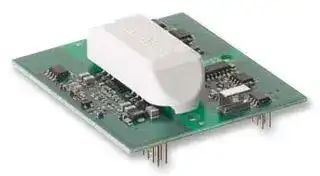
SKYPER 32 R
IGBT Driver, Half Bridge, 15 A, 14.4 V to 15.6 VPCB-40
⚠️ Reference pricing provided. In case of supply shortages, we will connect you with our trusted procurement partners to ensure your project's continuity.
- Manufacturer: SEMIKRON
- Product type:
- Driver Configuration:Half Bridge; Peak Output Current:15A; Supply Voltage Min:14.4V; Supply Voltage Max:15.6V; Driver Case Sty; Available until stocks are exhausted Alternative available
- SVHC: No SVHC (15-Jun-2015)
- IC Mounting: Through Hole
- Input Delay: 1.1µs
- No. of Pins: 40Pins
- Output Delay: 1.1µs
- Product Range: SKYPER Series
- IGBT Technology: -
- No. of Channels: 2Channels
- IGBT Termination: Solder
- IC Case / Package: PCB
- Power Dissipation: -
- Power Switch Type: IGBT
- IGBT Configuration: Dual [Half Bridge]
- Supply Voltage Max: 15.6V
- Supply Voltage Min: 14.4V
- Transistor Mounting: Through Hole
- Driver Configuration: Half Bridge
- Transistor Case Style: DIP
- Operating Temperature Max: 85°C
- Operating Temperature Min: -40°C
- Continuous Collector Current: -
- Collector Emitter Voltage Max: 1.7kV
- Collector Emitter Saturation Voltage: -
| Delivery and price | |
|---|---|
| Units per pack | 10 |
| Price | 78.6 € |
| Current stock | 10+ |
| Lead time | 30 days |
Datasheet

**SKYPER 32 R** ~~iiAiEiAEAEAEAEA—E—A—E—E—E—E—_—_—_—_—_~~ ## **SKYPER[®]** ## IGBT Driver Core ## **SKYPER 32 R** ## Preliminary Data ## **Features** - Two output channels - Integrated potential free power supply - Under voltage protection - Drive interlock top / bottom - Dynamic short circuit protection - Shut down input - Failure management - UL recognized, ROHS - IEC 60068-1 (climate) 40/085/56, no condensation and no dripping water permitted, non-corrosive, climate class 3K3 acc. EN60721 ## **Typical Applications*** - Driver for IGBT modules in bridge circuits in industrial application - DC bus voltage up to 1200V ## **Footnotes** with external high voltage diode Please Note: the isolation test is not performed as a series test at SEMIKRON and must be performed by the user according to VDE 0110-20 can be expanded to 6,3µQ with boost capacitors Isolation coordination in compliance with EN50178 PD2 Operating temperature is real ambient temperature around the driver core Degree of protection: IP00 ||**Absolute Maximum Ratings**| |---|---| ||**Symbol**<br>**Conditions**<br>**Values**<br>**Unit**| ||| ||Vs<br>Supply voltage primary<br>16<br>V| ||ViH<br>Input signal voltage (HIGH)<br>Vs + 0.3<br>V| ||ViL<br>Input signal voltage (LOW)<br>GND - 0.3<br>V<br>IoutPEAK<br>Output peak current<br>15<br>A<br>IoutAVmax<br>Output average current<br>50<br>mA<br>~~a~~| |fmax<br>Max. switching frequency<br>50<br>kHz<br>VCE<br>Collector emitter voltage sense across<br>the IGBT<br>1700<br>V<br>dv/dt<br>Rate of rise and fall of voltage<br>secondary to primary side<br>50<br>kV/µs<br>Visol IO<br>Isolation test voltage input - output (AC,<br>rms, 2s)<br>4000<br>V<br>VisolPD<br>Partial discharge extinction voltage,<br>rms,QPD≤ 10pC<br>1500<br>V<br>Visol12<br>Isolation test voltage output 1 - output 2<br>(AC, rms, 2s)<br>1500<br>V<br>RGon min<br>Minimum rating for external RGon<br>1.5<br>Ω<br>RGoff min<br>Minimum rating for external RGoff<br>1.5<br>Ω<br>Qout/pulse<br>Max. rating for output charge per pulse<br>2.5<br>µC<br>Top<br>Operating temperature<br>-40 ... 85<br>°C<br>Tstg<br>Storage temperature<br>-40 ... 85<br>°C<br>**Characteristics**<br>**Symbol**<br>**Conditions**<br>**min.**<br>**typ.**<br>**max.**<br>**Unit**<br>Vs<br>Supply voltage primary side<br>14.4<br>15<br>15.6<br>V<br>IS0<br>Supply current primary (no load)<br>80<br>mA<br>Supply current primary side (max.)<br>450<br>mA<br>Vi<br>Input signal voltage on / off<br>15 / 0<br>V<br>VIT+<br>Input treshold voltage HIGH<br>12.3<br>V<br>VIT-<br>input threshold voltage (LOW)<br>4.6<br>V<br>RIN<br>Input resistance (switching/HALT<br>signal)<br>10<br>kΩ<br>VG(on)<br>Turn on output voltage<br>15<br>V<br>VG(off)<br>Turn off output voltage<br>-7<br>V<br>fASIC<br>Asic system switching frequency<br>8<br>MHz<br>td(on)IO<br>Input-output turn-on propagation time<br>1.1<br>µs<br>td(off)IO<br>Input-output turn-off propagation time<br>1.1<br>µs<br>td(err)<br>Error input-output propagation time<br>5.4<br>7.9<br>µs<br>tpERRRESET<br>Error reset time<br>9<br>µs<br>tTD<br>Top-Bot interlock dead time<br>3<br>0<br>µs<br>Cps<br>Coupling capacitance prim sec<br>12<br>pF<br>w<br>weight<br>28<br>g<br>MTBF<br>2.5<br>106h<br>~~a~~<br>~~es ee~~<br>~~Pf~~<br>~~fd~~<br>~~a~~<br>~~ee~~<br>~~a~~<br>~~i~~<br>~~Se~~<br>~~aee~~<br>~~ns~~<br>~~aeeee~~<br>~~es~~<br>~~ee~~<br>~~i~~<br>~~eees ee a~~<br>~~Be~~<br>~~rs~~<br>~~ee~~<br>~~ae~~<br>~~a~~<br>~~Po~~<br>~~a_~~|| ||This is an electrostatic discharge sensitive device (ESDS), international standard IEC 60747-1,| ||Chapter IX| * The specifications of our components may not be considered as an assurance of component characteristics. Components have to be tested for the respective application. Adjustments may be necessary. The use of SEMIKRON products in life support appliances and systems is subject to prior specification and written approval by SEMIKRON. We therefore strongly recommend prior consultation of our staff. **Driver Core** ~~Ps~~ **© by SEMIKRON Rev. 6 – 27.05.2014 1** **SKYPER** ~~**[®]**~~ **32 R** ## **Technical Explanations** Revision 06 Status: Prepared by: Johannes Krapp _This Technical Explanation is valid for the following parts:_ |_part number:_|_L6100102_|_SKYPER 32 R_|_Standard type _| |---|---|---|---| ||_L6100103_|_SKYPER32/01 R_|_Standard type with coating_| |_date code (YYWW): _|_≥CW21 - 2014_||| ## **SKYPER[®] 32 R / SKYPER 32/01 R** ## **Content** Application and Handling Instructions ............................................................................................................ 2 Further application support ........................................................................................................................... 2 General Description ..................................................................................................................................... 2 Features of SKYPER 32 R UL ...................................................................................................................... 2 UL specified remarks ................................................................................................................................... 3 Block diagram ............................................................................................................................................. 3 Dimensions ................................................................................................................................................. 3 PIN Array – Primary Side ............................................................................................................................. 4 PIN Array – Secondary Side ......................................................................................................................... 5 Driver Performance ...................................................................................................................................... 6 Insulation .................................................................................................................................................... 6 Isolation Test Voltage................................................................................................................................... 7 Auxiliary Power Supply................................................................................................................................. 7 Under Voltage Protection of driver power supply (UVP) .................................................................................. 8 Input Signals ............................................................................................................................................... 8 Short Pulse Suppression (SPS) .................................................................................................................... 8 Failure Management .................................................................................................................................... 9 Shut Down Input (SDI) ................................................................................................................................. 9 Dead Time generation (Interlock TOP / BOT) (DT) ....................................................................................... 10 Dynamic Short Circuit Protection by VCEsat monitoring / de-saturation monitoring (DSCP) ............................... 10 Adjustment of DSCP .................................................................................................................................. 11 High Voltage Diode for DSCP ..................................................................................................................... 12 Gate resistors ............................................................................................................................................ 12 External Boost Capacitors (BC) .................................................................................................................. 13 Application Example .................................................................................................................................. 13 Mounting Notes ......................................................................................................................................... 14 Environmental Conditions........................................................................................................................... 14 Marking ..................................................................................................................................................... 15 **© by SEMIKRON** **Rev 6 – 27.05.2014** **1** **SKYPER** ~~**[®]**~~ **32 R** **Please note:** Unless otherwise specified, all values in this technical explanation are typical values. Typical values are the average values expected in large quantities and are provided for information purposes only. These values can and do vary in different applications. All operating parameters should be validated by user’s technical experts for each application. ~~a~~ ## **Application and Handling Instructions** - Please provide for static discharge protection during handling. As long as the hybrid driver is not completely assembled, the input terminals have to be short-circuited. Persons working with devices have to wear a grounded bracelet. Any synthetic floor coverings must not be statically chargeable. Even during transportation the input terminals have to be short-circuited using, for example, conductive rubber. Worktables have to be grounded. The same safety requirements apply to MOSFET- and IGBT-modules. - Any parasitic inductances within the DC-link have to be minimised. Over-voltages may be absorbed by C- or RCDsnubbers between main terminals for PLUS and MINUS of the power module. - When first operating a newly developed circuit, SEMIKRON recommends to apply low collector voltage and load current in the beginning and to increase these values gradually, observing the turn-off behaviour of the free-wheeling diode and the turn-off voltage spikes generated across the IGBT. An oscillographic control will be necessary. Additionally, the case temperature of the module has to be monitored. When the circuit works correctly under rated operation conditions, short-circuit testing may be done, starting again with low collector voltage. - It is important to feed any errors back to the control circuit and to switch off the device immediately in failure events. Repeated turn-on of the IGBT into a short circuit with a high frequency may destroy the device. - The inputs of the hybrid driver are sensitive to over-voltage. Voltages higher than VS +0,3V or below -0,3V may destroy these inputs. Therefore, control signal over-voltages exceeding the above values have to be avoided. - The connecting leads between hybrid driver and the power module should be as short as possible (max. 20cm), the driver leads should be twisted. ## **Further application support** Latest information is available at http://www.semikron.com. For design support please read the SEMIKRON Application Manual Power Modules available at http://www.semikron.com. ## **General Description** The SKYPER 32 core constitutes an interface between IGBT modules and the controller. The driver is developed according to the requirements of UL standard. This core is a half bridge driver. Basic functions for driving, potential separation and protection are integrated in the driver. Thus it can be used to build up a driver solution for IGBT modules. ## **Features of SKYPER 32 R** - Two output channels **==> picture [49 x 7] intentionally omitted <==** **----- Start of picture text -----**<br> SKYPER 32<br>**----- End of picture text -----**<br> - Integrated potential free power supply for the secondary side - - - - Short Pulse Suppression (SPS) - Under Voltage Protection (UVP) - Drive interlock (dead time) top / bottom (DT) - Dynamic Short Circuit Protection (DSCP) by VCE monitoring and direct switch off - - - - - Shut Down Input (SDI) - UL recognized, ROHS - Failure Management - Expandable by External Boost Capacitors (BC) - DC bus voltage up to 1200V **© by SEMIKRON** **Rev 6 – 27.05.2014** **2** **SKYPER** ~~**[®]**~~ **32 R** ## **UL specified remarks** - The equipment shall be installed in compliance with the mounting and spacing requirements of the end-use application. - SKYPER 32 shall be supplied by an isolated limited voltage / limited current source or a Class 2 source. The 15 A peak rating is an instantaneous peak rating only. - These devices do not incorporate solid-state motor overload protection. The need for overload protection and overcurrent protection devices shall be determined in the end-use product. - These devices have not been evaluated to over-voltage, over-current, and over-temperature control, and may need to be subjected to the applicable end-product tests. - Temperature and tests shall be considered in the end use. Due to the limited current source, only the effect of heat generating components in this device on adjacent components in the end product needs to be considered. - Connectors have not been evaluated field wiring; all connections are to be factory wired only. ## **Block diagram** ## **Block diagram** **==> picture [431 x 161] intentionally omitted <==** **----- Start of picture text -----**<br> Error Processing TOP SEC_TOP_VCE_CFG<br>- VCE monitoring SEC_TOP_VCE_IN<br>SEC_TOP_IGBT_ON<br>Power Driver SEC_TOP_IGBT_OFF<br>TOP SEC_TOP_15P<br>PRIM_TOP_IN SEC_TOP_8N<br>Signal Processing: Power SEC_TOP_GND<br>PRIM_BOT_IN - short pulse suppression Supply<br>- drive interlock top / bottom TOP<br>PRIM_nERROR_IN - under voltage protection Wet<br>PRIM_nERROR_OUT - error latch / output / input<br>Power<br>PRIM_PWR_15P DC/DC converter control SupplyBOT SEC_BOT_VCE_CFG<br>PRIM_PWR_GND SEC_BOT_VCE_IN<br>Power Driver SEC_BOT_IGBT_ON<br>BOT SEC_BOT_IGBT_OFF<br>SEC_BOT_15P<br>ael I = Error Processing BOT SEC_BOT_8N<br>- VCE monitoring SEC_BOT_GND<br>**----- End of picture text -----**<br> ## **Dimensions** **==> picture [486 x 290] intentionally omitted <==** **----- Start of picture text -----**<br> Dimensions in mm (bottom view) (top view)<br>51,15<br>49,90 24<br>24<br>14,34<br>a8<br>i<br>J E S<br>57 ±0,2<br>±0,2mm unless otherwise noted<br>3 Rev 6 – 27.05.2014 © by SEMIKRON<br>Ø 3,2<br>10,3<br>1 2<br>6,8 1 2<br>9,14 X10<br>9 10 X100 11,68<br>9 10 42,16<br>32<br>64 ±0,2<br>10,3<br>1 2<br>X200<br>6,8 9 10<br>max 19<br>**----- End of picture text -----**<br> **SKYPER** ~~**[®]**~~ **32 R** ## **PIN Array – Primary Side** **==> picture [497 x 166] intentionally omitted <==** **----- Start of picture text -----**<br> Connectors Connector X10 (RM2,54, 10pin)<br>SQ 0,64<br>2,54<br>±0,25mm unless otherwise noted<br>1 2<br>1 2<br>X10<br>9 10 X100<br>9 10<br>2,54 8,13 ±0,2<br>1 2<br>X200<br>9 10<br>**----- End of picture text -----**<br> |**PIN**|**Signal**|**Function**|**Specification**| |---|---|---|---| |X10:01|PRIM_PWR_GND|GND for power supply and GND for digital<br>signals|| |X10:02|PRIM_PWR_GND|GND for power supply and GND for digital<br>signals|| |X10:03|PRIM_nERROR_OUT|ERROR output|LOW = NO ERROR; open collector output;<br>max. 30V / 15mA<br>(external pull up resistor necessary)| |X10:04|PRIM_nERROR_IN|ERROR input|5V logic; LOW active| |X10:05|PRIM_PWR_GND|GND for power supply and GND for digital<br>signals|| |X10:06|PRIM_PWR_GND|GND for power supply and GND for digital<br>signals|| |X10:07|PRIM_TOP_IN|Switching signal input (TOP switch)|Digital 15 V; 10 kOhm impedance;<br>LOW = TOP switch off;<br>HIGH = TOP switch on| |X10:08|PRIM_BOT_IN|Switching signal input (BOTTOM switch)|Digital 15 V; 10 kOhm impedance;<br>LOW = BOT switch off;<br>HIGH = BOT switch on| |X10:09|PRIM_PWR_15P|Drive core power supply|Stabilised +15V ±4%| |X10:10|PRIM_PWR_15P|Drive core power supply|Stabilised +15V ±4%| **© by SEMIKRON** **Rev 6 – 27.05.2014** **4** **SKYPER** ~~**[®]**~~ **32 R** ## **PIN Array – Secondary Side** **==> picture [497 x 165] intentionally omitted <==** **----- Start of picture text -----**<br> Connectors Connector X100 / X200 (RM2,54, 10pin)<br>SQ 0,64<br>2,54<br>±0,25mm unless otherwise noted<br>1 2<br>1 2<br>X10<br>9 10 X100<br>9 10<br>2,54 8,13 ±0,2<br>1 2<br>X200<br>9 10<br>**----- End of picture text -----**<br> |**PIN**|**Signal**|**Function**|**Specification**| |---|---|---|---| |X100:01|SEC_TOP_VCE_CFG|Input reference voltage adjustment|| |X100:02|SEC_TOP_VCE_IN|Input VCEmonitoring|| |X100:03|SEC_TOP_15P|Output power supply for external buffer<br>capacitors|Stabilised +15V| |X100:04|SEC_TOP_15P|Output power supply for external buffer<br>capacitors|Stabilised +15V| |X100:05|SEC_TOP_GND|GND for power supply and GND for digital<br>signals|| |X100:06|SEC_TOP_IGBT_ON|Switch on signal TOP IGBT|| |X100:07|SEC_TOP_GND|GND for power supply and GND for digital<br>signals|| |X100:08|SEC_TOP_IGBT_OFF|Switch off signal TOP IGBT|| |X100:09|SEC_TOP_8N|Output power supply for external buffer<br>capacitors|Stabilised -7V| |X100:10|SEC_TOP_8N|Output power supply for external buffer<br>capacitors|Stabilised -7V| |X200:01|SEC_BOT_VCE_CFG|Input reference voltage adjustment|| |X200:02|SEC_BOT_VCE_IN|Input VCEmonitoring|| |X200:03|SEC_BOT_15P|Output power supply for external buffer<br>capacitors|Stabilised +15V| |X200:04|SEC_BOT_15P|Output power supply for external buffer<br>capacitors|Stabilised +15V| |X200:05|SEC_BOT_GND|GND for power supply and GND for digital<br>signals|| |X200:06|SEC_BOT_IGBT_ON|Switch on signal BOT IGBT|| |X200:07|SEC_BOT_GND|GND for power supply and GND for digital<br>signals|| |X200:08|SEC_BOT_IGBT_OFF|Switch off signal BOT IGBT|| |X200:09|SEC_BOT_8N|Output power supply for external buffer<br>capacitors|Stabilised -7V| |X200:10|SEC_BOT_8N|Output power supply for external buffer<br>capacitors|Stabilised -7V| **© by SEMIKRON** **Rev 6 – 27.05.2014** **5** **SKYPER** ~~**[®]**~~ **32 R** ## **Driver Performance** The driver is designed for application with half bridges or single modules and a maximum gate charge per pulse < 2,5µC (< 6,3µC with external boost capacitors). The charge necessary to switch the IGBT is mainly depending on the IGBT’s chip size, the DC-link voltage and the gate voltage. This correlation is shown in module datasheets. It should, however, be considered that the driver is turned on at +15V and turned off at -7V. Therefore, the gate voltage will change by 22V during each switching procedure. Unfortunately, many datasheets do not show negative gate voltages. In order to determine the required charge, the upper leg of the charge curve may be prolonged to +22V for determination of approximate charge per switch. The medium output current of the driver is determined by the switching frequency and the gate charge. The maximum switching frequency may be calculated with the shown equation and is limited by the average current of the driver power supply and the power dissipation of driver components. **==> picture [490 x 403] intentionally omitted <==** **----- Start of picture text -----**<br> Calculation Switching Frequency Maximum Switching Frequency @ different Gate Charges @ T amb=25°C<br>60 kHz<br>fmax IoutQAVGEmax 50 kHz40 kHz ~ \ \\<br>\<br>30 kHz \<br>fmax: Maximum switching frequency * \<br>IoutQGEAVmax: Gate charge of the driven IGBT : Maximum output average current 20 kHz \N Wy<br>* @ Tamb=25°C 10 kHz with external boost capacitors “iy<br>0 kHz<br>0 µC 1 µC 2 µC 3 µC 4 µC 5 µC 6 µC 7 µC<br>gate charge<br>Calculation Average Output Current Average Output Current as a Function of the Ambient Temperature<br>| |<br>60 mA<br>50 mA<br>Iout AV fsw QGE<br>40 mA<br>IoutAV: Average output current 30 mA |<br>fsw: Switching frequency l<br>QGE: Gate charge of the driven IGBT 20 mA |<br>l<br>10 mA |<br>0 mA _ NNN\N<br>0 °C 10 °C 20 °C 30 °C 40 °C 50 °C 60 °C 70 °C 80 °C 90 °C<br>ambient temperature<br>aie<br>Please note:<br>The maximum value of the switching frequency is limited to 50kHz due to switching reasons.<br>switching frequency<br>average output current<br>**----- End of picture text -----**<br> ## **Insulation** Magnetic transformers are used for insulation between gate driver primary and secondary side. The transformer set consists of pulse transformers which are used bidirectional for turn-on and turn-off signals of the IGBT and the error feedback between secondary and primary side, and a DC/DC converter. This converter provides a potential separation (galvanic separation) and power supply for the two secondary (TOP and BOT) sides of the driver. Thus, external transformers for external power supply are not required. **Creepage and Clearance Distance in mm** Primary to secondary Min. 12,2 **© by SEMIKRON** **Rev 6 – 27.05.2014** **6** **SKYPER** ~~**[®]**~~ **32 R** ## **Isolation Test Voltage** The isolation test voltage represents a measure of immunity to transient voltages. The maximum test voltage and time applied once between input and output, and once between output 1 and output 2 are indicated in the absolute maximum ratings. The high-voltage isolation tests and repeated tests of an isolation barrier can degrade isolation capability due to partial discharge. Repeated isolation voltage tests should be performed with reduced voltage. The test voltage must be reduced by 20% for each repeated test. The isolation of the isolation barrier (transformer) is checked in the part. With exception of the isolation barrier, no active parts, which could break through are used. An isolation test is not performed as a series test. Therefore, the user can perform once the isolation test with voltage and time indicated in the absolute maximum ratings. **Please note:** An isolation test is not performed at SEMIKRON as a series test. ## **Auxiliary Power Supply** A few basic rules should be followed when dimensioning the customer side power supply for the driver. The following table shows the required features of an appropriate power supply. |**Requirements of the auxiliary power supply**|| |---|---| |Regulated power supply|+15V ±4%| |Maximum rise time of auxiliary power supply|50ms| |Minimum peak current of auxiliary supply|1A| |Power on reset completed after|150ms| The supplying switched mode power supply may not be turned-off for a short time as consequence of its current limitation. Its output characteristic needs to be considered. Switched mode power supplies with fold-back characteristic or hiccup-mode can create problems if no sufficient over current margin is available. The voltage has to rise continuously and without any plateau formation as shown in the following diagram. ## **Rising slope of the power supply voltage** If the power supply is able to provide a higher current, a peak current will flow in the first instant to charge up the input capacitances on the driver. Its peak current value will be limited by the power supply and the effective impedances (e.g. distribution lines), only. It is recommended to avoid the paralleling of several customer side power supply units. Their different set current limitations may lead to dips in the supply voltage. The driver is ready for operation typically 150ms after turning on the supply voltage. The driver error signal PRIM_nERROR_OUT is operational after this time. Without any error present, the error signal will be reset. To assure a high level of system safety the TOP and BOT signal inputs should stay in a defined state (OFF state, LOW) during driver turn-on time. Only after the end of the power-on-reset, IGBT switching operation shall be permitted. **© by SEMIKRON** **Rev 6 – 27.05.2014** **7** **SKYPER** ~~**[®]**~~ **32 R** ## **Under Voltage Protection of driver power supply (UVP)** The internally detected supply voltage of the driver has an under voltage protection. The table below gives an overview of the trip level. |**Supply voltage**|**UVP level**| |---|---| |Regulated +15V ±4%|13,5V| If the internally detected supply voltage of the driver falls below this level, the IGBTs will be switched off (IGBT driving signals set to LOW). The input side switching signals of the driver will be ignored. The error memory will be set, and the output PRIM_nERROR_OUT changes to the HIGH state. ## **Input Signals** The signal transfer to each IGBT is made with pulse transformers, used for switching on and switching off of the IGBT. The inputs have a Schmitt Trigger characteristic and a positive / active high logic (input HIGH = IGBT on; input LOW = IGBT off). It is mandatory to use circuits which switch active to +15V and 0V. Pull up and open collector output stages must not be used for TOP / BOT control signals. It is recommended choosing the line drivers according to the demanded length of the signal lines. **Please note:** It is not permitted to apply switching pulses shorter than 1µs. **==> picture [497 x 127] intentionally omitted <==** **----- Start of picture text -----**<br> TOP / BOT Input<br>User Side A capacitor is connected to the input to obtain high noise immunity.<br>This capacitor can cause for current limited line drivers a little delay of<br>PRIM_TOP_IN INPUT TOP few ns, which can be neglected. The capacitors have to be placed as<br>close as possible to the driver interface.<br>PRIM_BOT_IN INPUT BOT<br>C C<br>1nF 1nF<br>PRIM_PWR_GND GND<br>PRIM_PWR_GND<br>**----- End of picture text -----**<br> ## **Short Pulse Suppression (SPS)** This circuit suppresses short turn-on and off-pulses of incoming signals. This way the IGBTs are protected against spurious noise as they can occur due to bursts on the signal lines. Pulses shorter than 625ns are suppressed and all pulses longer than 750ns get through for 100% probability. Pulses with a length in-between 625ns and 750ns can be either suppressed or get through. **==> picture [245 x 107] intentionally omitted <==** **----- Start of picture text -----**<br> Pulse pattern – SPS<br>short pulses<br>PRIM_TOP/BOT_IN (HIGH)<br>PRIM_TOP/BOT_IN (LOW)<br>SEC_TOP/BOT_IGBT_ON<br>SEC_TOP/BOT_IGBT_OFF<br>**----- End of picture text -----**<br> **© by SEMIKRON** **Rev 6 – 27.05.2014** **8** **SKYPER** ~~**[®]**~~ **32 R** ## **Failure Management** Any error detected will set the error latch and force the output PRIM_nERROR_OUT into HIGH state. Switching pulses from the controller will be ignored. Connected and switched off IGBTs remain turned off. The switched off IGBTs remain turned off. A reset of the latched error memory is only possible if no failure is present anymore and if the TOP and BOT input signals are set to the LOW level for a period of tpERRRESET > 9µs. The output PRIM_nERROR_OUT is an open collector output. For the error evaluation an external pull-up-resistor is necessary pulled-up to the positive operation voltage of the control logic (LOW signal = no error present, wire break safety is assured). **==> picture [499 x 204] intentionally omitted <==** **----- Start of picture text -----**<br> Open collector error transistor Application hints<br>An external resistor to the controller logic high level is required. The<br>User Side<br>resistor has to be in the range of V / Imax < Rpull_up < 10kΩ.<br>V PRIM_nERROR_OUT can operate to maximum 30V and can switch<br>a maximum of 15mA.<br>Rpull_up<br>Example:<br>PRIM_nERROR_OUT For V = +15V the needed resistor should be in the range<br>C Rpull_up = (15V/15mA) … 10kΩ 1kΩ… 10kΩ.<br>1nF<br>PRIM_PWR_GND GND<br>PRIM_PWR_GND<br>Please note:<br>The error output PRIM_ERROR_OUT is not short circuit proof.<br>**----- End of picture text -----**<br> ## **Shut Down Input (SDI)** The shut down input / error input signal can gather error signals of other hardware components for switching off the IGBT (input HIGH = no turn-off; input LOW = turn-off). A LOW signal at PRIM_nERROR_IN will set the error latch and force the output PRIM_nERROR_OUT into HIGH state. Switching pulses from the controller will be ignored. A reset of the latched error memory is only possible if no LOW signal at PRIM_nERROR_IN is present anymore and if the TOP and BOT input signals are set to the LOW level for a period of tpERRRESET > 9µs. The SDI function can be disabled by no connection or connecting to 5V. **==> picture [227 x 148] intentionally omitted <==** **----- Start of picture text -----**<br> Connection SDI<br>User Side<br>+5V<br>Rpull_up_int<br>3,3K<br>PRIM_nERROR_IN<br>C INPUT ERROR<br>1nF<br>PRIM_PWR_GND GND<br>PRIM_PWR_GND<br>**----- End of picture text -----**<br> **© by SEMIKRON** **Rev 6 – 27.05.2014** **9** **SKYPER** ~~**[®]**~~ **32 R** ## **Dead Time generation (Interlock TOP / BOT) (DT)** The DT circuit prevents, that TOP and BOT IGBT of one half bridge are switched on at the same time (shoot through). The dead time is not added to a dead time given by the controller. Thus the total dead time is the maximum of "built in dead time" and "controller dead time". It is possible to control the driver with one switching signal and its inverted signal. ## **Please note:** The generated dead time is fixed and cannot be changed. **==> picture [497 x 154] intentionally omitted <==** **----- Start of picture text -----**<br> Pulse pattern – DT<br>PRIM_TOP_IN (HIGH) The total propagation delay of the driver is the sum of<br>PRIM_TOP_IN (LOW) interlock dead time (tTD) and driver input output signal<br>PRIM_BOT_IN (HIGH) propagation delay (td(on;off)IO) as shown in the pulse pattern.<br>Moreover the switching time of the IGBT chip has to be taken<br>PRIM_BOT_IN (LOW) into account (not shown in the pulse pattern).<br>SEC_TOP_IGBT_ON<br> In case both channel inputs (PRIM_TOP_IN and<br>SEC_TOP_IGBT_OFF PRIM_BOT_IN) are at high level, the IGBTs will be turned off.<br>SEC_BOT_IGBT_ON<br> If only one channel is switching, there will be no interlock<br>SEC_BOT_IGBT_OFF dead time.<br>td(on;off)IO<br>tTD<br>**----- End of picture text -----**<br> **Please note:** No error message will be generated when overlap of switching signals occurs. ## **Dynamic Short Circuit Protection by VCEsat monitoring / de-saturation monitoring (DSCP)** The DSCP circuit is responsible for short circuit sensing. It monitors the collector-emitter voltage VCE of the IGBT during its on-state. Due to the direct measurement of VCEsat on the IGBT's collector, the DSCP circuit switches off the IGBTs and an error is indicated. The reference voltage VCEref may dynamically be adapted to the IGBTs switching behaviour. Immediately after turn-on of the IGBT, a higher value is effective than in steady state. This value will, however, be reset, when the IGBT is turned off. VCEstat is the steady-state value of VCEref and is adjusted to the required maximum value for each IGBT by an external resistor RCE. It may not exceed 10V. The time constant for the delay (exponential shape) of VCEref may be controlled by an external capacitor CCE, which is connected in parallel to RCE. It controls the blanking time tbl which passes after turn-on of the IGBT before the VCEsat monitoring is activated. This makes an adaptation to any IGBT switching behaviour possible. **==> picture [326 x 164] intentionally omitted <==** **----- Start of picture text -----**<br> Reference Voltage (VCEref) Characteristic<br>V<br>15<br>10<br>VCEref<br>VCEstat<br>5<br>VCE<br>VCEsat<br>0<br>t<br>turn on instant tbl<br>**----- End of picture text -----**<br> After tbl has passed, the VCE monitoring will be triggered as soon as VCE > VCEref and will turn off the IGBT. The error memory will be set, and the output PRIM_nERROR_OUT changes to the HIGH state. Possible failure modes are shows in the following pictures. **© by SEMIKRON** **Rev 6 – 27.05.2014** **10** **SKYPER** ~~**[®]**~~ **32 R** **==> picture [497 x 145] intentionally omitted <==** **----- Start of picture text -----**<br> Short circuit during operation Turn on of IGBT too slow * Short circuit during turn on<br>V V V<br>15 15 15<br>VCE<br>10 10 10<br>VCEref VCEref VCEref<br>VCEstat VCEstat VCEstat<br>5 VCE 5 VCE 5<br>VCEsat VCEsat VCEsat<br>0 0 0<br>turn on instant tbl t turn on instant tbl t turn on instant tbl t<br>**----- End of picture text -----**<br> * or adjusted blanking time too short ## **Adjustment of DSCP** The external components RCE and CCE are applied for adjusting the steady-state threshold the blanking time. **==> picture [497 x 303] intentionally omitted <==** **----- Start of picture text -----**<br> Connection RCE and CCE Dimensioning of RCE and CCE<br>R CE k 17k ln1 VCEstat R VCE kV <br>5,8V<br> [] []<br> <br>User Side<br>SEC_TOP_VCE_CFG<br>tbl s 5,2 s ,011 s RCE<br>RCE CCE CCE pF k <br> s<br>,000323<br>SEC_TOP_GND pF<br>SEC_TOP_GND<br>VCEstat: Collector-emitter threshold static monitoring voltage<br>tblx: Blanking time<br>SEC_BOT_VCE_CFG<br>RCE CCE VCEstat_max = 8V (RVCE = 0Ω)<br>VCEstat_max = 7V (RVCE = 1kΩ)<br>SEC_BOT_GND<br>SEC_BOT_GND<br>Please Note:<br>The equations are calculated considering the use of high voltage diode<br>BY203/20S. The calculated values V CEstat and tbl are typical values at room<br>temperature. These values can and do vary in the application (e.g. tolerances of<br>used high voltage diode, resistor RCE, capacitor CCE).<br>The DSCP function is not recommended for over current protection.<br>**----- End of picture text -----**<br> ## **Application hints** If the DSCP function is not used, for example during the experimental phase, SEC_TOP_VCE_IN must be connected with SEC_TOP_GND for disabling SCP @ TOP side and SEC_BOT_VCE_IN must be connected with SEC_BOT_GND for disabling SCP @ BOT side. **© by SEMIKRON** **Rev 6 – 27.05.2014** **11** **SKYPER** ~~**[®]**~~ **32 R** ## **High Voltage Diode for DSCP** The high voltage diode blocks the high voltage during IGBT off state. The connection of this diode between driver and IGBT is shown in the following schematic. **==> picture [497 x 204] intentionally omitted <==** **----- Start of picture text -----**<br> Connection High Voltage Diode Characteristics<br>User Side Reverse blocking voltage of the diode shall be higher than the<br>used IGBT.<br>RVCE BY203/20S<br>SEC_TOP_VCE_IN Reverse recovery time of the fast diode shall be lower than V CE<br>SEC_TOP_VCE_CFG rising of the used IGBT.<br>RCE CCE<br>SEC_TOP_GND TOP Forward voltage of the diode: 1,5V @ 2mA forward current (Tj=25°C).<br>SEC_TOP_GND<br>RVCE BY203/20S Load A collector series resistance RVCE (1kΩ / 0,4W) must be<br>SEC_BOT_VCE_IN connected for 1700V IGBT operation.<br>SEC_BOT_VCE_CFG<br>RCE CCE<br>SEC_BOT_GND BOT<br>SEC_BOT_GND<br>**----- End of picture text -----**<br> ## **Gate resistors** The output transistors of the driver are MOSFETs. The sources of the MOSFETs are separately connected to external terminals in order to provide setting of the turn-on and turn-off speed of each IGBT by the external resistors RGon and RGoff. As an IGBT has input capacitance (varying during switching time) which must be charged and discharged, both resistors will dictate what time must be taken to do this. The final value of the resistance is difficult to predict, because it depends on many parameters as DC link voltage, stray inductance of the circuit, switching frequency and type of IGBT. **==> picture [497 x 203] intentionally omitted <==** **----- Start of picture text -----**<br> Connection RGon, RGoff Application Hints<br>User Side The gate resistor influences the switching time, switching losses,<br>dv/dt behaviour, etc. and has to be selected very carefully. Due to<br>RGon TOP this influence a general value for the gate resistors cannot be<br>SEC_TOP_IGBT_ON recommended. The gate resistor has to be optimized according to<br>SEC_TOP_IGBT_OFF RGE switching behaviour and over voltage peaks within the specific<br>RGoff 10K circuitry.<br>SEC_TOP_GND Load<br>By increasing RGon the turn-on speed will decrease. The reverse<br>SEC_TOP_GND<br>peak current of the free-wheeling diode will diminish.<br>SEC_BOT_IGBT_ON RGon BOT By increasing RGoff the turn-off speed of the IGBT will decrease. The<br>inductive peak over voltage during turn-off will diminish.<br>SEC_BOT_IGBT_OFF RGoff R10KGE In order to ensure locking of the IGBT even when the driver supply<br>SEC_BOT_GND voltage is turned off, a resistance (RGE) has to be integrated.<br>SEC_BOT_GND<br>**----- End of picture text -----**<br> **Please note:** Do not connect the terminals SEC_TOP_IGBT_ON with SEC_TOP_IGBT_OFF and SEC_BOT_IGBT_ON with SEC_BOT_IGBT_OFF, respectively. **© by SEMIKRON** **Rev 6 – 27.05.2014** **12** **SKYPER** ~~**[®]**~~ **32 R** ## **External Boost Capacitors (BC)** The rated gate charge of the driver may be increase by additional boost capacitors to drive IGBT with large gate capacitance. **==> picture [497 x 224] intentionally omitted <==** **----- Start of picture text -----**<br> Connection External Boost Capacitors Dimensioning of Cboost<br>User Side Cboost15P [µF] = QGE [µC] × 1/V - 2,2µF<br>SEC_TOP_PWR_15P Cboost8N [µF] = QGE [µC] × 2/V - 4,7µF<br>SEC_TOP_PWR_15P<br> QGE: Gate charge of the IGBT @ VGE = -7 …+15V<br>SEC_TOP_PWR_8N<br>SEC_TOP_PWR_8N Minimum rated voltage Cboost15P: 25V<br>Cboost8N Cboost15P<br>SEC_TOP_GND Minimum rated voltage Cboost8N: 16V<br>SEC_TOP_GND<br> Type of capacitor: ceramic capacitor<br>SEC_BOT_PWR_15P Please consider the maximum rating four output charge per<br>SEC_BOT_PWR_15P pulse of the gate driver.<br>SEC_BOT_PWR_8N<br>Application Hints<br>SEC_BOT_PWR_8N<br>Cboost8N Cboost15P<br>SEC_BOT_GND The external boost capacitors should be connected as close as<br>SEC_BOT_GND possible to the gate driver and to have low inductance.<br>**----- End of picture text -----**<br> ## **Application Example** ## **Connection Schematic** **==> picture [497 x 294] intentionally omitted <==** **----- Start of picture text -----**<br> DC+<br>SKYPER [TM] 32 SEC_TOP_VCE_CFG BY203/20S<br>SEC_TOP_VCE_IN<br>SEC_TOP_15P 18k 330pF<br>50V<br>SEC_TOP_15P<br>SEC_TOP_GND<br>Ron<br>SEC_TOP_IGBT_ON<br>4,75k PRIM_PWR_GND SEC_TOP_GND<br>PRIM_PWR_GND<br>SEC_TOP_IGBT_OFF 10k<br>ERROR OUT PRIM_nERROR_OUT Roff<br>PRIM_nERROR_IN SEC_TOP_8N 4,7µF 2,2µF<br>SEC_TOP_8N 16V 25V<br>PRIM_PWR_GND<br>PRIM_PWR_GND<br>SEC_BOT_VCE_CFG BY203/20S load<br>INPUT TOP PRIM_TOP_IN<br>SEC_BOT_VCE_IN<br>INPUT BOT PRIM_BOT_IN SEC_BOT_15P 18k 330pF<br>PRIM_PWR_15P 50V<br>SEC_BOT_15P<br>+15V PRIM_PWR_15P<br>SEC_BOT_GND<br>1nF 1nF 1nF 1nF 220µF Ron<br>100V 100V 100V 100V 35V SEC_BOT_IGBT_ON<br>SEC_BOT_GND<br>SEC_BOT_IGBT_OFF 10k<br>Roff<br>SEC_BOT_8N 4,7µF 2,2µF<br>SEC_BOT_8N 16V 25V<br>DC-<br>- application example for 1200V IGBT<br>- Qout/pulse = 5µC<br>- VCEref = 5,5V<br>- tbl = 5,5µs<br>**----- End of picture text -----**<br> **© by SEMIKRON** **Rev 6 – 27.05.2014** **13** **SKYPER** ~~**[®]**~~ **32 R** ## **Mounting Notes** **==> picture [497 x 132] intentionally omitted <==** **----- Start of picture text -----**<br> Soldering Hints Finished Hole & Pad Size in mm<br>The temperature of the solder must not exceed 260°C, and solder time must Ø 1,1 ±0,05<br>not exceed 10 seconds.<br>The ambient temperature must not exceed the specified maximum storage<br>temperature of the driver.<br>The solder joints should be in accordance to IPC A 610 Revision D (or later) -<br>pad size: min. 1,8<br>Class 3 (Acceptability of Electronic Assemblies) to ensure an optimal<br>connection between driver core and printed circuit board.<br>**----- End of picture text -----**<br> **Please note:** The driver is not suited for hot air reflow or infrared reflow processes. The connection between driver core and printed circuit board should be mechanical reinforced by using support posts. **==> picture [497 x 167] intentionally omitted <==** **----- Start of picture text -----**<br> Use of Support Posts<br>SKYPER 32 Product information of suitable support posts and<br>distributor contact information is available at e.g.<br>http://www.richco-inc.com (e.g. series DLMSPM,<br>LCBST).<br>When using the support posts the support post length<br>Support post<br>has to be longer than 12,4mm.<br>Printed Ciruit Board<br>**----- End of picture text -----**<br> ## **Please note:** The use of agressive materials in cleaning and potting process of driver core may be detrimental for the device parameters. If the driver core is coated by the user, any warranty (Gewährleistung) expires. ## **Environmental Conditions** The driver core is type tested under the environmental conditions below. |**Conditions**|**Values (max.)**| |---|---| |Vibration|Sinusoidal sweep 20Hz … 500Hz, 5g, 26 sweeps per axis (x, y, z)<br>-<br>Tested acc. IEC 68-2-6<br>-<br>Connection between driver core and printed circuit board mechanical reinforced by using support posts.| |Shock|Half-sinusoidal pulse, 5g, shock width 18ms, 3 shocks in each direction (±x, ±y, ±z), 18 shocks in total<br>-<br>Tested acc. IEC 68-2-27<br>-<br>Connection between driver core and printed circuit board mechanical reinforced by using support posts.| The characteristics and further environmental conditions are indicated in the data sheet. **© by SEMIKRON** **Rev 6 – 27.05.2014** **14** **SKYPER** ~~**[®]**~~ **32 R** ## **Marking** Every driver core is marked. The marking contains the following items. ## **DISCLAIMER** SEMIKRON reserves the right to make changes without further notice herein to improve reliability, function or design. Information furnished in this document is believed to be accurate and reliable. However, no representation or warranty is given and no liability is assumed with respect to the accuracy or use of such information. SEMIKRON does not assume any liability arising out of the application or use of any product or circuit described herein. Furthermore, this technical information may not be considered as an assurance of component characteristics. No warranty or guarantee expressed or implied is made regarding delivery, performance or suitability. This document supersedes and replaces all information previously supplied and may be superseded by updates without further notice. SEMIKRON products are not authorized for use in life support appliances and systems without the express written approval by SEMIKRON. **www.SEMIKRON.com** **© by SEMIKRON** **Rev 6 – 27.05.2014** **15**
Updated at March 31, 2026
About Novapart
Novapart is a B2B electronic component broker specialising in stock shortages and cost reduction. We source hard-to-find parts and identify compliant alternatives across a catalogue of 410,000+ components from 500+ manufacturers.
Learn more →Stock Shortage Specialist
When a component is unavailable, discontinued or has an unacceptable lead time, we tap into our network of vetted European and Asian distributors to source what you need — without compromising on quality or traceability.
Request a quote →Compliant Alternatives
We identify pin-to-pin, electrically equivalent substitutes that meet the same certifications (RoHS, AEC-Q100, REACH) as your original specification — validated against datasheets, not just part numbers. Often at a lower cost.
BOM Analysis service →