
Image not available
Illustrative purposes only

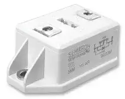
SKM111AR
Power MOSFET, N Channel, 100 V, 200 A, 0.007 ohm, SEMITRANS M1, Module
⚠️ Reference pricing provided. In case of supply shortages, we will connect you with our trusted procurement partners to ensure your project's continuity.
- Manufacturer: SEMIKRON
- Product type: Single MOSFETs
- No. of Pins: 4Pins
- Channel Type: N Channel
- Power Dissipation: 700W
- Transistor Mounting: Module
- Transistor Polarity: N Channel
- Power Dissipation Pd: 700W
- Rds(on) Test Voltage: 10V
- On Resistance Rds(on): 0.007ohm
- Transistor Case Style: SEMITRANS M1
- Drain Source Voltage Vds: 100V
- Operating Temperature Max: 150°C
- Continuous Drain Current Id: 200A
- Drain Source On State Resistance: 0.007ohm
- Gate Source Threshold Voltage Max: 3V
| Delivery and price | |
|---|---|
| Units per pack | 50 |
| Price | 67.36 € |
| Current stock | 10+ |
| Lead time | 30 days |
Datasheet

## **SKM 111AR** MOSFET,TRANSISTOR

> **Absolute Maximum Ratings** T, = 25 °C, unless otherwise specified —- **Symbol** | **Conditions** | **Values** | **Units** a Vos 100 Vv f SN at Ip T, = 25 (80) °C 200 (150) A

> "@ke4 2sed“ - VesTy» (Tstg) 1ms - 40 ... +260+ 150 **0** (125) °CVvA ot Visol AC, 1 min. 2500 v **Inverse diode** In =-ly 200 A **SEMITRANS[TM] M1** lem =~ Ign 600 A Power MOSFET Modules **Characteristics** T, = 25 °C, unless otherwise specified Vier)pss **Symbol** - **Conditions** =0V, Ip = 0,25 mA | **min.** 100 **typ. max.** | **Units** Vv **SKM 111AR** Vesith) Ves = Vos: Ip = 1 mA 21 3 4 Vv loss Veg = 0 V, Vpg = 100 V, 50(300) 250(1000) | pA T, = 25 (125) °C loss Veg = 20 V, Vpg = OV 10 100 nA Rosyon) Veg = 10 V, Ip = 130A 7 8,5 ma **Features** Os Vos = 25 V, Ip = 130A 60 75 Ss e« NChannel, enhancement mode =| Ccxc Ves = 9, Vos = 25 V, f= 1 MHz 160 pF e Avalanche characteristic Ciss 10 13 nF e Short connections and built-in coe 3 i rr gate resistors to suppress internal L , 50 aH oscillations even in critical ~~DS~~ applications ton) Vpp = 50 V, Ip = 130A, 60 ns e Isolated copper baseplate r Ves == 10V, Rg = 3,3 0 oo ° All electrical connections on top “o 500 - for easy busbaring ~~f~~ e Large clearances (10 mm) and **Inverse diode** creepage distances (20 mm) Vsp Ip = 400 A; Veg = OV 1,25 1,6 Vv + UL recognized, file no. E 63532 |‘ T= 28 (050) °C 400 ns Q, T, = 25°C 3,5 uC **Typical Applications*** lie T, = 150 °C A e Switched mode power supplies **Thermal characteristics** e DC servo and robot drives Reng-c) per MOSFET 0,18 K/IW e DC choppers Rinic-s) M,, surface 10 ym, per module 0,05 K/W e UPS equipment **Mechanical data** e Not suitable for linear M, to heatsink (M6) 4 5 Nm amplification M, for terminals (M5) 2,5 3,5 Nm w 130 g **MA**

© by SEMIKRON

1

21-12-2015 DIL

## **SKM 111AR** MOSFET,TRANSISTOR

Fig. 1 Rated power dissipation vs. temperature

**==> picture [129 x 8] intentionally omitted <==**

**----- Start of picture text -----**<br>
Fig. 2 Maximum safe operating area<br>**----- End of picture text -----**<br>


**==> picture [96 x 8] intentionally omitted <==**

**----- Start of picture text -----**<br>
Fig. 3 Output characteristic<br>**----- End of picture text -----**<br>


**==> picture [102 x 8] intentionally omitted <==**

**----- Start of picture text -----**<br>
Fig. 4 Transfer characteristic<br>**----- End of picture text -----**<br>


**==> picture [131 x 8] intentionally omitted <==**

**----- Start of picture text -----**<br>
Fig. 5 On-resistance vs. temperature<br>**----- End of picture text -----**<br>


**==> picture [130 x 8] intentionally omitted <==**

**----- Start of picture text -----**<br>
Fig. 6 Rated current vs. temperature<br>**----- End of picture text -----**<br>


© by SEMIKRON

2

21-12-2015 DIL

## **SKM 111AR** MOSFET,TRANSISTOR

Fig. 7 Brakdown voltage vs. temperature

Fig. 8 Drain-source voltage derating

**==> picture [13 x 9] intentionally omitted <==**

**----- Start of picture text -----**<br>
nC<br>**----- End of picture text -----**<br>


**==> picture [159 x 8] intentionally omitted <==**

**----- Start of picture text -----**<br>
Fig. 9 Capacitances vs. drain-source voltage<br>**----- End of picture text -----**<br>


Fig. 11 Diode forward characteristic

Fig. 10 Gate charge characteristic

Fig. 14 Gate-source threshold voltage

© by SEMIKRON

3

21-12-2015 DIL

## **SKM 111AR** MOSFET,TRANSISTOR

**==> picture [344 x 16] intentionally omitted <==**

**----- Start of picture text -----**<br>
UL Recognized Dimensions in mm<br>File no. E 63 532<br>**----- End of picture text -----**<br>


This is an electrostatic discharge sensitive device (ESDS), international standard IEC 60747-1, chapter IX.

## *IMPORTANT INFORMATION AND WARNINGS

The specifications of SEMIKRON products may not be considered as guarantee or assurance of product characteristics ("Beschaffenheitsgarantie"). The specifications of SEMIKRON products describe only the usual characteristics of products to be expected in typical applications, which may still vary depending on the specific application. Therefore, products must be tested for the respective application in advance. Application adjustments may be necessary. The user of SEMIKRON products is responsible for the safety of their applications embedding SEMIKRON products and must take adequate safety measures to prevent the applications from causing a physical injury, fire or other problem if any of SEMIKRON products become faulty. The user is responsible to make sure that the application design is compliant with all applicable laws, regulations, norms and standards. Except as otherwise explicitly approved by SEMIKRON in a written document signed by authorized representatives of SEMIKRON, SEMIKRON products may not be used in any applications where a failure of the product or any consequences of the use thereof can reasonably be expected to result in personal injury. No representation or warranty is given and no liability is assumed with respect to the accuracy, completeness and/or use of any information herein, including without limitation, warranties of non-infringement of intellectual property rights of any third party. SEMIKRON does not assume any liability arising out of the applications or use of any product; neither does it convey any license under its patent rights, copyrights, trade secrets or other intellectual property rights, nor the rights of others. SEMIKRON makes no representation or warranty of noninfringement or alleged non-infringement of intellectual property rights of any third party which may arise from applications. Due to technical requirements our products may contain dangerous substances. For information on the types in question please contact the nearest SEMIKRON sales office. This document supersedes and replaces all information previously supplied and may be superseded by updates. SEMIKRON reserves the right to make changes.

~~Lo~~ 4 21-12-2015 DIL © by SEMIKRON
Updated at February 9, 2023
About Novapart
Novapart is a B2B electronic component broker specialising in stock shortages and cost reduction. We source hard-to-find parts and identify compliant alternatives across a catalogue of 410,000+ components from 500+ manufacturers.
Learn more →Stock Shortage Specialist
When a component is unavailable, discontinued or has an unacceptable lead time, we tap into our network of vetted European and Asian distributors to source what you need — without compromising on quality or traceability.
Request a quote →Compliant Alternatives
We identify pin-to-pin, electrically equivalent substitutes that meet the same certifications (RoHS, AEC-Q100, REACH) as your original specification — validated against datasheets, not just part numbers. Often at a lower cost.
BOM Analysis service →