
Image not available
Illustrative purposes only

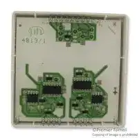
SKHI 22A H4 R
IGBT Driver, Half Bridge, 8 A, 14.4 V to 15.6 V, Module
⚠️ Reference pricing provided. In case of supply shortages, we will connect you with our trusted procurement partners to ensure your project's continuity.
- Manufacturer: SEMIKRON
- Product type:
- Driver Configuration:Half Bridge; Peak Output Current:8A; Supply Voltage Min:14.4V; Supply Voltage Max:15.6V; Driver Case Style:Module; No. of Pins:-; Input Delay:1µs; Output Delay:1µs;
- SVHC: No SVHC (15-Jun-2015)
- Input Delay: 1µs
- Output Delay: 1µs
- Product Range: SEMIDRIVER Series
- IGBT Technology: -
- IGBT Termination: Solder
- IC Case / Package: Module
- Power Dissipation: -
- Power Switch Type: IGBT
- IGBT Configuration: Dual [Half Bridge]
- Supply Voltage Max: 15.6V
- Supply Voltage Min: 14.4V
- Transistor Mounting: Surface Mount
- Driver Configuration: Half Bridge
- Transistor Case Style: SMD
- Operating Temperature Max: 85°C
- Operating Temperature Min: -40°C
- Continuous Collector Current: -
- Collector Emitter Voltage Max: 1.7kV
- Collector Emitter Saturation Voltage: -
| Delivery and price | |
|---|---|
| Units per pack | 10 |
| Price | 125.39 € |
| Current stock | 25+ |
| Lead time | 30 days |
Datasheet

## **SKHI 21A (R) ...**

|||||**Absolute Maximum Ratings**|**Absolute Maximum Ratings**||||||||||
|---|---|---|---|---|---|---|---|---|---|---|---|---|---|---|
|||ae.<br>ead||**Symbol**<br>Vg<br>Vin|**Conditions**<br>|Supplyvoltageprim.<br>Inputsignal volt. (High)||||||**Values**<br>18<br>Vg+ 0,3|||||**Units**<br>Vv<br>Vv|
|||||loutpeaK|Output peak current|||||8||||A|
|||||l0Uty ymax|Output average current|||||40||||mA|
|||||fax|max. switching frequency|||||50||||kHz|
|||||VoE|Collector emittervoltage sense across|||||1200||||Vv|
||||||the IGBT||||||||||
|||**SEMIDRIVERTM**||dv/dt<br>Visollo|Rate of rise and fall ofvoltage secondary<br>to primary side<br>Isolation testvoltage<br>input - output (2 sec. AC)|||||50<br>2500||||kV/us<br>Vac|
|Hybrid Dual MOSFET||||Visolt2|Isolation test voltage<br>output 1 - output 2 (2 sec. AC)|||||1500||||Vv|
|Driver||||Reonmin<br>Reotmin|Minimum rating for Reo,<br>Minimum rating forReo|||||3<br>3||||Q<br>Q|
|**SKHI 21A (R)**||||Qoutipulse<br>Top|Max. rating foroutputcharge per pulse<br>Operating temperature|||||4’)<br>-40...<br>+ 85||||uC<br>°C|
|||||Tstg|Storage temperature|||||-40... + 85||||°C|
||||||||||||||||
|**Features**<br>e drivesMOSFETswith||||**Characteristics**<br>**Symbol**<br>**Conditions**<br>Vs<br>wontvoltageprimaryside||T, <br>||||**min.**<br>**typ.**<br>**max.**<br>**Units**<br> = 25 °C, unless otherwise specified<br>14,4<br>15<br>15,6<br>|<br>Vv||||||
|e||Vpsvony < 10V<br>is compatible to old SKHI 21||Iso|Supplycurrent primary side (no load)<br>Supply current primary side (max.)|||||80|290|||mA<br>mA|
|e||CMOS compatible inputs||V;|Input signal voltage on/off|||||15/0||||Vv|
|**Typical Applications**<br>e Short circuit potection byVoce<br>monitoring and switch off<br>e Drive interlocktop / bottom<br>q<br>e Isolation bytransformers<br>P Supply undervotage<br>protection (13 V)<br>~~e Error latch / output~~<br>e DriverforMOSFET modules in<br>bridge circuits in industrial||||Vite<br>Vir.<br>Rin<br>V,<br>yo<br>Gloff)<br>Reg<br>fasic<br>taonyio<br>tacotnio<br>taern<br>toerrreser <br>trp|Inputthreshold voltage (High)<br>Inputthreshold voltage (Low)<br>Inputresistance<br>Turnon gatevoltage output<br>r<br>urn offgatevoltage output<br>Internal gate-emitter resistance<br>Asicsystem switchingfrequency<br>Input-output turn-on propagation time<br>Input-output turn-offpropagation time<br>Error input-output propagation time<br> |Etrorresettime<br>Top-Bot Interlock Dead Time||||4,5<br>0,85<br>0,85|10<br>+15<br>0<br>22<br>8<br>1<br>1<br>0,6<br>9<br>4,3|12,5<br>1,15<br>1,15|||Vv<br>Vv<br>Ko<br>Vv<br>Vv<br>kQ<br>MHz<br>us<br>us<br>Us<br>us<br>us|
|||applications||VoeEsat|ReferencevoltageforV.--monitoring|||||5?)|10|||Vv|
|1)<br>2)||see fig. 6<br>:<br>AtRog= 18kQ,Cog=330pF||Cos<br>MTBF<br>Ww|Coupling capacitance primarysecondary<br>MeanTimeBetween FailureT, =40°C<br>weight|||||12<br>2,0<br>45||||pF<br>10°h<br>g|
||||||||||||||||
|||||This technical information specifies semiconductor devices but promises no|||||||||||
|||||characteristics. No warranty or guarantee expressed or implied is made regarding|||||||characteristics. No warranty or guarantee expressed or implied is made regarding||||
|||||delivery, performance or suitability.|||||||||||


© by SEMIKRON

30-09-2008 MHW

1

**SKHI 22 A / B (R) ...**

|||||**Absolute Maximum Ratings**|**Absolute Maximum Ratings**|**Absolute Maximum Ratings**|**Absolute Maximum Ratings**|||||||||
|---|---|---|---|---|---|---|---|---|---|---|---|---|---|---|---|
|||ae.<br>ead||**Symbol**<br>Vg<br>Vin||Supply||**Conditions**<br>Supplyvoltageprim.<br>Inputsignal volt. (High) SKHI22A|||||**Values**<br>18<br>Vg+ 0,3|||||**Units**<br>Vv<br>Vv|
||||||||SKHI 22B||||5+ 0,3||||Vv|
|||||loutpEaK|||Output peak current||||8||||A|
|||||loutaymax|||Output average current||||40||||mA|
|||||fax|||max. switching frequency||||50||||kHz|
|||||VoE|||Collector emittervoltage sense across||||1200||||Vv|
||||||||the IGBT|||||||||
||**SEMIDRIVERTM**|||dv/dt|||Rate of rise and fall ofvoltage secondary<br>to primary side||||50||||kV/us|
|||||Visollo|||Isolation testvoltage||||2500||||Vac|
|Hybrid Dual IGBT Driver||||Visolt2|||input - output (2 sec. AC)<br>Isolation test voltage||||1500||||Vv|
||||||||output 1 - output 2 (2 sec. AC)|||||||||
|||||Reonmin|||Minimum rating for Reo,||||3||||Q|
|**SKHI 22 A / B (R)**||**SKHI 22 A / B (R)**||Reotmin<br>Qoutpulse|||Minimum rating forReo<br>Max. rating foroutputcharge perpulse||||3<br>4’)||||Q<br>uC|
|||||Top|||Operating temperature||||-40...<br>+ 85||||°C|
|||||Tstg|||Storage temperature||||-40... + 85||||°C|
|||||||||||||||||
|||||||||||||||||
|**Features**<br>eDoubledriver||driverforhalfbridge||**Characteristics**<br>|||||T, <br>|||= 25 °C,|unless otherwise specified<br>||||||
|e|eDoubledriver|driverforhalfbridge||**Symbol**|||||**Conditions**|||||**min.**|**typ.**|**max.**|||||**Units**|


## **Typical Applications**

- 1) 2)

This technical information specifies semiconductor devices but promises no characteristics. No warranty or guarantee expressed or implied is made regarding delivery, performance or suitability.

© by SEMIKRON

30-09-2008 MHW

1

## **SKHI 22 A / B H4 (R) ...**

## **SEMIDRIVER[TM]**

**==> picture [152 x 15] intentionally omitted <==**

**----- Start of picture text -----**<br>
Hybrid Dual IGBT Driver<br>**----- End of picture text -----**<br>


**SKHI 22 A / B H4 (R)**

## **Features**

**==> picture [362 x 274] intentionally omitted <==**

**----- Start of picture text -----**<br>
||||||||||||
|---|---|---|---|---|---|---|---|---|---|---|
|Absolute Maximum Ratings|
|Vg|Symbol|| Supply|Conditions|voltage prim.|||Values|18|||Units|Vv|
|Vin|Input signal|volt.|(High)|SKHI 22A H4|Vg +|0,3|Vv|
|SKHI|22B|H4|5+|0,3|Vv|
|loutpEaK|Output|peak|current|8|A|
|louta ymax|Output|average|current|40|mA|
|fax|max.|switching|frequency|50|kHz|
|VoE|Collector emitter voltage|sense|across|1700|Vv|
|the|IGBT|
|dv/dt|Rate|of|rise|and|fall|of voltage|secondary|50|kV/us|
|to|primary|side|
|Visollo|Isolation|test voltage|4000|Vac|
|input|-|output|(2|sec.|AC)|
|Visolt2|Isolation|test|voltage|1500|Vv|
|output|1|-|output|2|(2|sec.|AC)|
|Reonmin|Minimum|rating|for|Reo,|3|Q|
|Reotmin|Minimum|rating|for Reo|3|Q|
|Qoutpulse|Max.|rating|for output charge|per pulse|4’)|uC|
|Top|Operating|temperature|- 40...|+|85|°C|
|T stg|Storage|temperature|- 40...|+|85|°C|
|Characteristics|T,|=|25|°C,|unless|otherwise|specified|
|Symbol|||Conditions|||min.|typ.|max.|||Units|

**----- End of picture text -----**<br>


## **Typical Applications** e Driver for IGBT modules circuits in industrial o ~~BIG bus MAES ie~~ 1) see fig. 6 2)

This technical information specifies semiconductor devices but promises no characteristics. No warranty or guarantee expressed or implied is made regarding delivery, performance or suitability.

© by SEMIKRON

30-09-2008 MHW

1

## **External Components**

|**Component**|**Function**|**Recommended Value**|
|---|---|---|
|RCE|Reference voltage for VCE-monitoring<br>with RVCE= 1kΩ(1700V IGBT):<br>VCEstat V<br>(<br>)<br>10 RCE kΩ<br>(<br>)<br>⋅<br>10<br>RCE kΩ<br>(<br>)<br>+<br>----------------------------------**-**<br>1,4              (1)<br>–<br>=<br>VCEstat V<br>(<br>)<br>10 RCE kΩ<br>(<br>)<br>⋅<br>10<br>RCE kΩ<br>(<br>)<br>+<br>----------------------------------**-**<br>1,8            (1.1)<br>–<br>=|10kΩ< RCE< 100kΩ<br>18kΩfor SKM XX 123 (1200V)<br>36kΩfor SKM XX 173 (1700V)|
|CCE|Inhibit time for VCE- monitoring<br>tmin<br>τCE<br>15<br>VCEstat V<br>(<br>)<br>–<br>10<br>VCEstat V<br>(<br>)<br>–<br>--------------------------------------**-** (2)<br>ln<br>⋅<br>=<br>τCE μs<br>(<br>)<br>CCE nF<br>(<br>)<br>10 RCE kΩ<br>(<br>)<br>⋅<br>10<br>RCE kΩ<br>(<br>)<br>+<br>----------------------------------**-**(3)<br>⋅<br>=|CCE< 2,7nF<br>0,33nF for SKM XX 123 (1200V)<br>0,47nF for SKM XX 173 (1700V)<br>0,5μs < tmin< 10μs|
|RVCE|Collector series resistance for  1700V<br>IGBT-operation|1kΩ/ 0,4W|
|RERROR|Pull-up resistance at error output<br>UPull<br>Up<br>–<br>RERROR<br>-----------------------<br>15mA<br><|1kΩ< RERROR< 10kΩ|
|RGON|Turn-on speed of the IGBT4)|RGON> 3Ω|
|RGOFF|Turn-off speed of the IGBT5)|RGOFF> 3Ω|


4) Higher resistance reduces free-wheeling diode peak recovery current, increases IGBT turn-on time.

5) Higher resistance reduces turn-off peak voltage, increases turn-off time and turn-off power dissipation

**© by SEMIKRON 30-09-2008**

**Driver Electronic – PCB Drivers**

**2**

## **PIN array**

Fig. 2 shows the pin arrays. The input side (primary side) comprises 10 inputs (SKHI 22A / 21A 8 inputs), forming the interface to the control circuit (see fig.1).

The output side (secondary side) of the hybrid driver shows two symmetrical groups of pins with 4 outputs, each forming the interface to the power module. All pins are designed for a grid of 2,54 mm.

## **Primary side PIN array**

|**PIN No. **|**Designation**|**Explanation**|
|---|---|---|
|P14|GND / 0V|related earth connection for input signals|
|P13|VS|+ 15V±4% voltage supply|
|P12|VIN1|switching signal input 1 (TOP switch)<br>positive 5V logic (for SKHI22A /21A, 15V logic)|
|P11|free|not wired|
|P10|/ERROR|error output,  low = error;  open collector output; max 30V / 15mA<br>(for SKHI22A /21A, internal 10kΩpull-up resistor versus VS)|
|P9|TDT2|signal input for digital adjustment of interlocking time;<br>**SKHI22B: to be switched by bridge to GND (see fig. 3)**<br>**SKHI22A /21A: to be switched by bridge to VS**|
|P8|VIN2|switching signal input 2 (BOTTOM switch);<br>positive 5V logic (for SKHI22A /21A, 15V logic)|
|P7|GND / 0V|related earth connection for input signals|
|P6|SELECT|signal input for neutralizing locking function;<br>to be switched by bridge to GND|
|P5|TDT1|signal input for digital adjustment of locking time;<br>to be switched by bridge to GND|


**ATTENTION:** Inputs P6 and P5 are not existing for SKHI 22A/ 21A. The contactor tracks of the digital input signals P5/ P6/ P9 must not be longer than 20 mm to avoid interferences, if no bridges are connected.

## **Secondary side PIN array**

|**PIN No.**|**Designation**|**Explanation**|
|---|---|---|
|S20|VCE1|collector output IGBT 1(TOP switch)|
|S15|CCE1|reference voltage adjustment with RCEand CCE|
|S14|GON1|gate 1 RONoutput|
|S13|GOFF1|gate 1 ROFFoutput|
|S12|E1|emitter output IGBT 1(TOP switch)|
|S1|VCE2|collector output IGBT 2(BOTTOM switch)|
|S6|CCE2|reference voltage adjustment with RCEand CCE|
|S7|GON2|gate 2 RONoutput|
|S8|GOFF2|gate 2 ROFFoutput|
|S9|E2|emitter output IGBT 2(BOTTOM switch)|


**ATTENTION:** The connector leads to the power module should be as short as possible.

**30-09-2008 © by SEMIKRON**

**Driver Electronic – PCB Drivers**

**3**

**==> picture [422 x 658] intentionally omitted <==**

**----- Start of picture text -----**<br>
ae<br>;<br>LOAD<br>output1 (TOP) output2 (BOTTOM<br>3 1 2<br>VCE<br>R CE * CE<br>4 5 6 7 SEMITRANS IGBT-Module<br>* C VCE C<br>R<br>* *<br>* CE * CE<br>CE R Ron Roff CE R Ron Roff<br>V V<br>output<br>S20 S15 S14 S13 S12 S1 S6 S7 S8 S9<br>Power driver Power driver<br>over over<br>current current<br>secondary side<br>= =<br>= =<br>S<br>Isolation S<br>V<br>V<br>-Vs monitor -Error monitor -Error memory<br>-input buffer-short pulse supression-pulse shaper primary side<br>-interlock -deadtime<br>integrated in ASIC<br>3k2<br>3k2<br>S S<br>V<br>V<br>*<br>*<br>6k8/100 P12 6k8/100 P8 P7 P14 P9 P5 P6 * P10 P13<br>iT iB VS<br>V V input<br>TDT2 TDT1<br>*<br>* Error<br>* SELECT<br>GND/OV GND/OV *<br>*<br>input1 (TOP) input2(BOTTOM) *<br>V ERROR<br>R<br>**----- End of picture text -----**<br>


**© by SEMIKRON 30-09-2008**

**Driver Electronic – PCB Drivers**

**4**

**==> picture [526 x 625] intentionally omitted <==**

**----- Start of picture text -----**<br>
VCE<br>OUT1<br>CCE<br>GND/0V GON<br>VS GOFF<br>V IN1 E<br>ERROR<br>TDT2 E<br>V IN2 GOFF<br>GND/0V GON<br>SELECT CCE<br>TDT1<br>OUT2<br>VCE<br>55 ±0.2 detail "A" on scale 10 : 1<br>50.8 ±0.3 0.25x0.5<br>measured from pin-centre to pin-centre A<br>15.75 18.25<br>S1<br>P5<br>P6 S6<br>S9<br>S12<br>P13<br>P14 S15<br>A<br>A<br>S20<br>R2<br>Date - Code<br>55<br>9.5<br>16 15<br>3.5<br>3.37<br>13.53<br>22.86<br>2.54 48.26<br>SKHI XX Y<br>±0.2<br>±0.5<br>±0.3<br>±0.3<br>**----- End of picture text -----**<br>


Fig. 2 Dimension drawing and PIN array (P5 and P6 are not existing for SKHI22A/21A)

**30-09-2008 © by SEMIKRON**

**Driver Electronic – PCB Drivers**

**5**

## **SEMIDRIVER[TM]**

## **SKHI 22A / 22B und SKHI 21A**

## **Hybrid dual drivers**

The driver generation SKHI 22A/B and SKHI 21A will replace the hybrid drivers SKHI 21/22 and is suitable for all available low and medium power range IGBT and MOSFETs.

The SKHI 22A (SKHI 21A) is a form-, fit- and mostly function-compatible replacement to its predecessor, the SKHI 22 (SKHI 21).

The SKHI 22B is recommended for any new development. It has two additional signal pins on the primary side with which further functions may be utilized.

The SKHI 22A and SKHI 22B are available with standard isolation (isolation testing voltage 2500 VAC, 2sec.) as well as with an increased isolation voltage (type "H4") (isolation testing voltage 4000 VAC, 2sec.). The SKHI 21A is only offered with standard isolation features.

## **Differences SKHI 22-22A (SKHI 21-21A)**

Compared to the old SKHI 22/21 the new driver SKHI 22A / 21A is absolutely compatible with regards to pins and mostly with regards to functions. It may be equivalently used in existing PCBs.

## **The following points have to be considered when exchanging the drivers:**

- **Leave out the two resistors RTD for interlocking dead time adjustment at pin 11 and pin 9.**

- **The interlocking time of the driver stages in halfbridge applications is adjusted to 3,25 µs. It may be increased up to 4,25 µs by applying a 15 V (VS) supply voltage at Pin 9 (TDT2) (wire bridge)**

- **The error reset time is typically 9µs.**

- **The input resistance is 10 k** Ω **.**

As far as the SKHI 22A is concerned, the negative gate voltage required for turn-off of the IGBT is no longer -15V, but -7V.

## **General description**

The new driver generation SKHI 22A/B, SKHI 21A consists of a hybrid component which may directly be mounted to the PCB.

All devices necessary for driving, voltage supply, error monitoring and potential separation are integrated in the driver. In order to adapt the driver to the used power module, only very few additional wiring may be necessary.

The forward voltage of the IGBT is detected by an integrated short-circuit protection, which will turn off the module when a certain threshold is exceeded.

In case of short-circuit or too low supply voltage the integrated error memory is set and an error signal is generated.

The driver is connected to a controlled + 15 V-supply voltage. The input signal level is 0/15 V for the SKHI 22A/ 21A and 0/5 V for the SKHI 22B.

In the following explanations the whole driver family will be designated as SKHI 22B. If a special type is referred to, the concerned driver version will explicitly be named.

## **Technical explanations[1]**

## **Description of the circuit block diagram and the functions of the driver**

The block diagram (fig.1) shows the inputs of the driver (primary side) on the left side and the outputs (secondary side) on the right.

## **The following functions are allocated to the primary side:**

**Input-Schmitt-trigger, CMOS compatible** , positive logic (input high = IGBT on)

## **Interlock circuit and deadtime generation of the IGBT**

If one IGBT is turned on, the other IGBT of a halfbridge cannot be switched. Additionally, a digitally adjustable interlocking time is generated by the driver (see fig. 3), which has to be longer than the turn-off delay time of the IGBT. This is to avoid that one IGBT is turned on before the other one is not completely discharged. This protec-tion-function may be neutralized by switching the select input (pin6) (see fig. 3). fig. 3 documents possible interlock-times. "High" value can be achieved with no connection and connection to 5 V as well.

|P6 ;<br>SELECT|P5 ;<br>TDT1|P9 ;<br>TDT2|interlock time<br>tTD/μs|
|---|---|---|---|
|open / 5V|GND|GND|1,3|
|open / 5V|GND|open / 5V|2,3|
|open / 5V|open / 5V|GND|3,3|
|open / 5V|open / 5V|open / 5V|4,3|
|GND|X|X|no interlock|


Fig. 3 SKHI 22B - Selection of interlock-times: „High“-level can be achieved by no connection or connecting to 5 V

## **Short pulse suppression**

The integrated short pulse suppression avoids very short switching pulses at the power semiconductor caused by high-frequency interference pulses at the driver input signals. Switching pulses shorter than 500 ns are suppressed and not transmitted to the IGBT.

## **Power supply monitoring (VS)**

A controlled 15 V-supply voltage is applied to the driver. If it falls below 13 V, an error is monitored and the error output signal switches to low level.

1.The following descriptions apply to the use of the hybrid driver for IGBTs as well as for power MOSFETs. For the reason of shortness, only IGBTs will be mentioned in the following. The designations "collector" and "emitter" will refer to IGBTs, whereas for the MOSFETs "drain" and "source" are to be read instead.

**© by SEMIKRON 30-09-2008**

**Driver Electronic – PCB Drivers 6**

## **Error monitoring and error memory**

The error memory is set in case of under-voltage or short-circuit of the IGBTs. In case of short-circuit, an error signal is transmitted by the VCE-input via the pulse transformers to the error memory. The error memory will lock all switching pulses to the IGBTs and trigger the error output (P10) of the driver. The error output consists of an open collector transistor, which directs the signal to earth in case of error. SEMIKRON recommends the user to provide for a pull-up resistor directly connected to the error evaluation board and to adapt the error level to the desired signal voltage this way. The open collector transistor may be connected to max. 30 V / 15 mA. If several SKHI 22Bs are used in one device, the error terminals may also be paralleled.

**ATTENTION:** Only the SKHI 22A / 21A is equipped with an internal pull-up resistor of 10 kΩ versus VS. The SKHI 22B does not contain an internal pull-up resistor.

The error memory may only be reset, if no error is pending and both cycle signal inputs are set to low for > 9 μs at the same time.

## **Pulse transformer set**

The transformer set consists of two pulse transformers one is used bidirectional for turn-on and turn-off signals of the IGBT and the error feedback between primary and secondary side, the other one for the DC/DC-converter. The DC/DC-converter serves as potential-separation and power supply for the two secondary sides of the driver. The isolation voltage for the "H4"-type is 4000 VAC and 2500 VAC for all other types.

## **The secondary side consists of two symmetrical driver switches integrating the following components:**

## **Supply voltage**

The voltage supply consists of a rectifier, a capacitor, a voltage controller for - 7 V and + 15 V and a + 10 V reference voltage.

## **Gate driver**

The output transistors of the power drivers are MOSFETs. The sources of the MOSFETs are separately connected to external terminals in order to provide setting of the turn-on and turn-off speed by the external resistors RON and ROFF. Do not connect the terminals S7 with S8 and S13 with S14, respectively. The IGBT is turned on by the driver at + 15 V by RON and turned off at - 7 V by ROFF. RON and ROFF may not chosen below 3 Ω. In order to ensure locking of the IGBT even when the driver supply voltage is turned off, a 22 kΩ-resistor versus the emitter output (E) has been integrated at output GOFF.

## **VCE-monitoring**

The VCE-monitoring controls the collector-emitter voltage VCE of the IGBT during its on-state. VCE is internally limited to 10 V. If the reference voltage VCEref is exceeded, the IGBT will be switched off and an error is indicated. The reference voltage VCEref may dynamically be adapted to the IGBTs switching behaviour. Immediately after turn-on of the IGBT, a higher value is effective than in the steady state. This value will, however, be reset, when the

IGBT is turned off. VCEstat is the steady-state value of VCEref and is adjusted to the required maximum value for each IGBT by an external resistor RCE to be connected between the terminals CCE (S6/S15) and E (S9/S12). It may not exceed 10 V. The time constant for the delay of VCEref may be increased by an external capacitor CCE, which is connected in parallel to RCE. It controls the time tmin which passes after turn-on of the IGBT before the VCE-monitoring is activated. This makes possible any adaptation to the switching behavior of any of the IGBTs. After tmin has passed, the VCE-monitoring will be triggered as soon as VCE > VCEref and will turn off the IGBT.

## **External components and possible adjustments of the hybrid driver**

Fig. 1 shows the required external components for adjustment and adaptation to the power module.

## **VCE - monitoring adjustment**

The external components RCE and CCE  are applied for adjusting the steady-state threshold and the short-circuit monitoring dynamic. RCE and CCE are connected in parallel to the terminals CCE  (S15/ S6) and E (S12/ S9) .

**==> picture [255 x 134] intentionally omitted <==**

**----- Start of picture text -----**<br>
8<br>7<br>6<br>5 1200V (min)<br>4 1200V (typ)<br>1200V (max)<br>3<br>1700V (min)<br>2 1700V (typ)<br>1 1700V (max)<br>0<br>10 20 30 RCE / kOhm 40 50<br> / V<br>CEstat<br>V<br>**----- End of picture text -----**<br>


Fig. 4 VCEstat in dependence of RCE (Tamb = 25°C)

Dimensioning of RCE and CCE can be done in three steps:

1. Calculate the maximum forward voltage from the datasheet of the used IGBT and determine VCEstat

2. Calculate approximate value of RCE according to equation (1) or (1.1) from VCEstat or determine RCE by using fig.4.

3. Determine tmin and calculate CCE according to equations (2) and (3).

Typical values are

for 1200 V IGBT: VCEstat = 5 V; tmin = 1,45 μs, RCE = 18 kΩ, CCE = 330 pF for 1700 V IGBT: VCEstat = 6 V; tmin = 3 μs, RCE = 36 kΩ, CCE = 470 pF

## **Adaptation to 1700 V IGBT**

When using 1700 V IGBTs it is necessary to connect a 1 kΩ / 0,4 W adaptation resistor between the VCE-terminal (S20/ S1) and the respective collector.

**30-09-2008 © by SEMIKRON**

**7 Driver Electronic – PCB Drivers**

## **Adaptation to error signal level**

An open collector transistor is used as error terminal, which, in case of error, leads the signal to earth. The signal has to be adapted to the evaluation circuit's voltage level by means of an externally connected pull-up resistor. The maximum load applied to the transistor shall be 30 V / 15 mA.

As for the SKHI 22A / 21A a 10 kΩ pull-up resistor versus VS (P13) has already been integrated in the driver.

## **IGBT switching speed adjustment**

The IGBT switching speed may be adjusted by the resistors RON and ROFF. By increasing RON the turn-on speed will decrease. The reverse peak current of the free-wheeling diode will diminish. SEMIKRON recommends to adjust RON to a level that will keep the turn-on delay time td(on) of the IGBT < 1 μs.

By increasing ROFF the turn-off speed of the IGBT will decrease. The inductive peak overvoltage during turn-off will diminish.

The minimum gate resistor value for ROFF and RON is 3 Ω. Typical values for RON and ROFF recommended by SEMIKRON are given in fig. 5

|SK-IGBT-Modul|RGon<br>Ω|RGoff<br>Ω|CCE<br>pF|RCE<br>kΩ|RVCE<br>kΩ|
|---|---|---|---|---|---|
|SKM 50GB123D|22|22|330|18|0|
|SKM 75GB123D|22|22|330|18|0|
|SKM 100GB123D|15|15|330|18|0|
|SKM 145GB123D|12|12|330|18|0|
|SKM 150GB123D|12|12|330|18|0|
|SKM 200GB123D|10|10|330|18|0|
|SKM 300GB123D|8,2|8,2|330|18|0|
|SKM 400GA123D|6,8|6,8|330|18|0|
|||||||
|SKM 75GB173D|15|15|470|36|1|
|SKM 100GB173D|12|12|470|36|1|
|SKM 150GB173D|10|10|470|36|1|
|SKM 200GB173D|8,2|8,2|470|36|1|


Fig. 5 Typical values for external components

## **Interlocking time adjustment**

Fig. 3 shows the possible interlocking times between output1 and output2. Interlocking times are adjusted by connecting the terminals TDT1 (P5), TDT2 (P9) and SELECT (P6) either to earth/ GND (P7 and P14) according to the required function or by leaving them open.

A typical interlocking time value is 3,25 μs (P9 = GND; P5 and P6 open). For SKHI 22A / 21A the terminals TDT1 (P5) and SELECT (P6) are not existing. The interlocking time has been fixed to 3,25 μs and may only be increased to 4,25 μs by connecting TDT2 (P9) to VS (P13).

**ATTENTION:** If the terminals TDT1 (P5), TDT2 (P9) and SELECT (P6) are not connected, eventually connected track on PC-board may not be longer than 20 mm in order to avoid interferences.

SEMIKRON recommends to start-up operation using the values recommended by SEMIKRON and to optimize the values gradually according to the IGBT switching behaviour and overvoltage peaks within the specific circuitry.

## **Driver performance and application limits**

The drivers are designed for application with halfbridges and single modules with a maximum gate charge QGE < 4 μC (see fig. 6).

The charge necessary to switch the IGBT is mainly depending on the IGBT's chip size, the DC-link voltage and the gate voltage.

This correlation is also shown in the corresponding module datasheet curves.

It should, however, be considered that the SKHI 22B is turned on at + 15 V and turned off at - 7 V. Therefore, the gate voltage will change by 22 V during every switching procedure.

Unfortunately, most datasheets do not indicate negative gate voltages. In order to determine the required charge, the upper leg of the charge curve may be prolonged to + 22 V for determination of approximate charge per switch.

The medium output current of the driver is determined by the switching frequency and the gate charge. For the SKHI 22B the maximum medium output current is IoutAVmax < ± 40 mA.

The maximum switching frequency fMAX may be calculated with the following formula, the maximum value however being 50 kHz due to switching reasons:

**==> picture [125 x 32] intentionally omitted <==**

Fig. 6 shows the maximum rating for the output charge per pulse for different gate resistors.

**==> picture [239 x 139] intentionally omitted <==**

**----- Start of picture text -----**<br>
SKHI 22 A/B maximum rating for output charge per<br>pulse<br>4,50<br>4,00<br>3,50 Rg=24  OHM; 3,86µC<br>3,00 Rg=18 OHM; 3,52µC<br>2,50<br>Rg=12 OHM; 3,07µC<br>2,00<br>1,50 Rg=6 OHM, 2,50µC<br>1,00 Rg=3 OHM, 2,18µC<br>0,50<br>0,00<br>0 10 20 30 40 50 60<br>f / kHz<br>Q / µC<br>**----- End of picture text -----**<br>


Fig. 6 Maximum rating for output charge per pulse

## **Further application notes**

The CMOS-inputs of the hybrid driver are extremely sensitive to over-voltage. Voltages higher than VS + 0,3 V or below – 0,3 V may destroy these inputs. Therefore, control signal over-voltages exceeding the above values have to be avoided.

Please provide for static discharge protection during handling. As long as the hybrid driver is not completely assembled, the input terminals have to be short-circuited.

**© by SEMIKRON 30-09-2008**

**Driver Electronic – PCB Drivers 8**

Persons working with CMOS-devices have to wear a grounded bracelet. Any synthetic floor coverings must not be statically chargeable. Even during transportation the input terminals have to be short-circuited using, for example, conductive rubber. Worktables have to be grounded. The same safety requirements apply to MOSFET- and IGBT-modules!

The connecting leads between hybrid driver and the power module should be as short as possible, the driver leads should be twisted.

Any parasitic inductances within the DC-link have to be minimized. Over-voltages may be absorbed by C- or RCD-snubbers between the main terminals for PLUS and MINUS of the power module.

When first operating a newly developed circuit, SEMIKRON recommends to apply low collector voltage and load current in the beginning and to increase these values gradually, observing the turn-off behaviour of the free-wheeling diode and the turn-off voltage spikes generated accross the IGBT. An oscillographic control will be necessary. In addition to that the case temperature of the module has to be monitored. When the circuit works correctly under rated operation conditions, short-circuit testing may be done, starting again with low collector voltage.

It is important to feed any errors back to the control circuit and to switch off the device immediately in such events. Repeated turn-on of the IGBT into a short circuit with a high frequency may destroy the device.

## **Mechanical fixing on PCB:**

In applications with mechanical vibrations do not use a ty-rap for fixing the driver, but - after soldering and testing - apply special glue. Recommended types: CIBA GEIGY XP 5090 + 5091; PACTAN 5011; WACKER A33 (ivory) or N199 (transparent), applied around the case edge (forms a concave mould). The housing may not be pressed on the PCB; do not twist the PCB with the driver soldered on, otherwise the internal ceramics may crack. The driver is not suitable for big PCBs.

Proven, within the scope of the product qualification, was the use of the driver with the printed circuit board SKPC 2006 ( L x B x H = 97,0 x 67,5 x 1,5 mm). During the test, the driver was stuck with glue on the printed circuit board. Based on this information the technical conclusion arises, that in an application with big printed circuit boards, this board must be supported and reinforced in the area of the driver.

If a PCB is directly plugged to IGBT modules, the PCB has to be fixed to the heat sink by thread bolts.

The temperature of the solder must not exceed 265°C, and solder time must not exceed 4 seconds. The ambient temperature must not exceed the specified maximum storage temperature of the driver.

The driver is not suited for hot air reflow or infrared reflow soldering processes.

## **Storage hints**

- Store driver only in original packaging. - Avoid contamination of driver's surface during storage, handling and processing.

- Please use the driver within one year after driver manufacturing date. The manufacturing date is marked on the driver. Usage of the driver beyond this shelf life could compromise product long term reliability.

- Further storage conditions are indicated in the data sheet

## **Environmental conditions**

The driver is type tested under the environmental conditions below.

Thermal cycling test:

- 100 cycle -40°C … +85°C

Vibration test according DIN IEC 68-2-6:

- Sinusoidal sweep: 10 Hz … 100 Hz

- -1 Octave / min.

- -Acceleration: 1,5 g

- -Axes: 3 (x, y, z)

- -26 sweeps per axis

- -Driver soldered on board SKPC 2006 (L x B x H = 97,0 x 67,5 x 1,5mm)

- -Driver stuck with glue on printed circuit board (see application notes)

Shock test according DIN IEC 68-2-27:

- Half-sinusoidal pulse

- -Peak acceleration: 5 g

- -Shock width: 18ms

- -3 shocks in each direction (±x, ±y und ±z)

- -18 shocks in total

- -Driver soldered on board SKPC 2006 (L x B x H = 97,0 x 67,5 x 1,5mm)

- -Driver stuck with glue on printed circuit board (see application notes)

**30-09-2008 © by SEMIKRON**

**Driver Electronic – PCB Drivers**

**9**

Temperature humidity according IEC 60068-1 (climate):

- 40/085/56 (40°C, 85% RH, 56h)

- No condensation, no dripping water, non- corrosive

- Climate class 3K3

All electrical and mechanical parameters should be validated by user´s technical experts for each application.

For further details please contact SEMIKRON.

This technical information specifies devices but promises no characteristics. No warranty or guarantee expressed or implied is made regarding delivery, performance or suitability.

**© by SEMIKRON 30-09-2008**

**Driver Electronic – PCB Drivers**

**10**
Updated at March 31, 2026
About Novapart
Novapart is a B2B electronic component broker specialising in stock shortages and cost reduction. We source hard-to-find parts and identify compliant alternatives across a catalogue of 410,000+ components from 500+ manufacturers.
Learn more →Stock Shortage Specialist
When a component is unavailable, discontinued or has an unacceptable lead time, we tap into our network of vetted European and Asian distributors to source what you need — without compromising on quality or traceability.
Request a quote →Compliant Alternatives
We identify pin-to-pin, electrically equivalent substitutes that meet the same certifications (RoHS, AEC-Q100, REACH) as your original specification — validated against datasheets, not just part numbers. Often at a lower cost.
BOM Analysis service →