
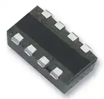


SI5513CDC-T1-GE3
Dual MOSFET, Complementary N and P Channel, 20 V, 20 V, 4 A, 4 A, 0.045 ohm
- Manufacturer: VISHAY
- Product type: Dual MOSFETs
- SVHC: No SVHC (04-Feb-2026)
- No. of Pins: 8Pins
- Channel Type: Complementary N and P Channel
- Product Range: Trench Series
- Qualification: -
- Transistor Case Style: ChipFET
- Operating Temperature Max: 150°C
- Power Dissipation N Channel: 3.1W
- Power Dissipation P Channel: 3.1W
- Drain Source Voltage Vds N Channel: 20V
- Drain Source Voltage Vds P Channel: 20V
- Continuous Drain Current Id N Channel: 4A
- Continuous Drain Current Id P Channel: 4A
- Drain Source On State Resistance N Channel: 0.045ohm
- Drain Source On State Resistance P Channel: 0.045ohm
| Delivery and price | |
|---|---|
| Units per pack | 5000 |
| Price | 0.175 € |
| Current stock | 1000+ |
| Lead time | 30 days |
**Si5513CDC**

**==> picture [59 x 49] intentionally omitted <==**

## Vishay Siliconix

## **N- and P-Channel 20 V (D-S) MOSFET**

**==> picture [43 x 92] intentionally omitted <==**

**==> picture [277 x 217] intentionally omitted <==**

**----- Start of picture text -----**<br>
PRODUCT SUMMARY<br> •<br>VDS (V) RDS(on) ( Ω ) ID (A) [a] Qg (Typ.)<br>0.055 at VGS = 4.5 V  4 [g]  •<br>N-Channel 20 0.085 at VGS = 2.5 V  4 [g] 2.6 nC  •<br> •<br>0.150 at VGS = - 4.5 V  - 3.7<br>P-Channel - 20 3.6 nC<br>0.255 at VGS = - 2.5 V  - 2.9<br>1206-8 ChipFET [®]  •<br>1<br>S1<br>D1 G1<br>D1 S2 Marking Code<br>D2 G2 EG XXX Lot Traceability<br>D2 and Date Code<br>Part # Code<br>Bottom View<br>**----- End of picture text -----**<br>


## **FEATURES**

- **Halogen-free According to IEC 61249-2-21 Definition**

- TrenchFET[®] Power MOSFETs

- 100 % R Tested g

- Compliant to RoHS Directive 2002/95/EC

## **APPLICATIONS**

- Load Switch for Portable Devices

**==> picture [181 x 120] intentionally omitted <==**

**----- Start of picture text -----**<br>
D1 S2<br>G2<br>G1<br>S1 D2<br>N-Channel MOSFET P-Channel MOSFET<br>**----- End of picture text -----**<br>


**Ordering Information:** Si5513CDC-T1-E3 (Lead (Pb)-free) Si5513CDC-T1-GE3 (Lead (Pb)-free and Halogen-free)

## **ABSOLUTE MAXIMUM RATINGS** TA = 25 °C, unless otherwise noted

|**ABSOLUTE MAXIMUM RATINGS**TA= 25 °C, unless otherwise noted|**ABSOLUTE MAXIMUM RATINGS**TA= 25 °C, unless otherwise noted|**ABSOLUTE MAXIMUM RATINGS**TA= 25 °C, unless otherwise noted|**ABSOLUTE MAXIMUM RATINGS**TA= 25 °C, unless otherwise noted|**ABSOLUTE MAXIMUM RATINGS**TA= 25 °C, unless otherwise noted|**ABSOLUTE MAXIMUM RATINGS**TA= 25 °C, unless otherwise noted|**ABSOLUTE MAXIMUM RATINGS**TA= 25 °C, unless otherwise noted|**ABSOLUTE MAXIMUM RATINGS**TA= 25 °C, unless otherwise noted|
|---|---|---|---|---|---|---|---|
|**Parameter**||**Symbol**|**N-Channel**||**P-Channel**||**Unit**|
|Drain-Source Voltage||VDS|20||- 20||V|
|Gate-Source Voltage||VGS|± 12|||||
|Continuous Drain Current (TJ= 150 °C)|TC= 25 °C|ID|4g||- 3.7||A|
||TC= 70 °C||4g||- 3.0|||
||TA= 25 °C||4b, c, g||-2.4b, c|||
||TA= 70 °C||3.5b, c||-1.9b, c|||
|Pulsed Drain Current||IDM|10||- 8|||
|Source Drain Current Diode Current|TC= 25 °C|IS|2.6||- 2.6|||
||TA= 25 °C||1.4b, c||-1.7b, c|||
|Maximum Power Dissipation|TC= 25 °C|PD|3.1||3.1||W|
||TC= 70 °C||2.0||2.0|||
||TA= 25 °C||1.7b, c||1.3b, c|||
||TA= 70 °C||1.1b, c||0.8b, c|||
|OperatingJunction and Storage Temperature Range||TJ, Tstg|- 55 to 150||||°C|
|SolderingRecommendations (Peak Temperature)d, e|||260|||||
|||||||||
|**THERMAL RESISTANCE RATINGS**||||||||
|**Parameter**||**Symbol**|**N-Channel**||**P-Channel**||**Unit**|
||||**Typ.**|**Max.**|**Typ.**|**Max.**||
|Maximum Junction-to-Ambientb, f|t≤5 s|RthJA|62|74|77|95|°C/W|
|Maximum Junction-to-Foot(Drain)|SteadyState|RthJF|32|40|33|40||


Notes:

a. Based on TC = 25 °C.

b. Surface mounted on 1" x 1" FR4 board.

c. t = 5 s.

- d. See Reliability Manual for profile. The ChipFET is a leadless package. The end of the lead terminal is exposed copper (not plated) as a result of the singulation process in manufacturing. A solder fillet at the exposed copper tip cannot be guaranteed and is not required to ensure adequade bottom side solder interconnection.

e. Rework conditions: manual soldering with a soldering iron is not recommended for leadless components.

- f. Maximum under steady state conditions is 115 °C/W  for N-Channel and 130 °C/W for P-Channel.

g. Package limited.

Document Number: 68806 S10-0547-Rev. C, 08-Mar-10

www.vishay.com 1

**Si5513CDC**

## Vishay Siliconix

**==> picture [59 x 48] intentionally omitted <==**

|**SPECIFICATIONS**TJ= 25 °C, unless otherwise noted|**SPECIFICATIONS**TJ= 25 °C, unless otherwise noted|**SPECIFICATIONS**TJ= 25 °C, unless otherwise noted||||||
|---|---|---|---|---|---|---|---|
|**Parameter**|**Symbol**|**Test Conditions**||**Min.**|**Typ.**|**Max.**|**Unit**|
|**Static**||||||||
|Drain-Source Breakdown Voltage|VDS|VGS= 0 V, ID= 250 µA|N-Ch<br>P-Ch|20|||V|
|||VGS= 0 V, ID= - 250 µA||- 20||||
|VDSTemperature Coefficient|ΔVDS/TJ|ID= 250 µA|N-Ch<br>P-Ch||23.7||mV/°C|
|||ID= - 250 µA|||- 19.5|||
|VGS(th)Temperature Coefficient|ΔVGS(th)/TJ|ID= 250 µA|N-Ch<br>P-Ch||- 3.5|||
|||ID= - 250 µA|||2.8|||
|Gate Threshold Voltage|VGS(th)|VDS= VGS, ID= 250 µA|N-Ch<br>P-Ch|0.6||1.5|V|
|||VDS= VGS, ID= - 250 µA||- 0.6||- 1.5||
|Gate-Body Leakage|IGSS|VDS= 0 V, VGS= ± 12 V|N-Ch<br>P-Ch|||100|nA|
|||||||- 100||
|Zero Gate Voltage Drain Current|IDSS|VDS= 20 V, VGS= 0 V|N-Ch<br>P-Ch|||1|µA|
|||VDS= - 20 V, VGS= 0 V||||- 1||
|||VDS= 20 V, VGS= 0 V, TJ= 55 °C|N-Ch<br>P-Ch|||10||
|||VDS= - 20 V, VGS= 0 V, TJ= 55 °C||||- 10||
|On-State Drain Currentb|ID(on)|VDS≥5 V, VGS= 4.5 V|N-Ch<br>P-Ch|10|||A|
|||VDS≤- 5 V, VGS= - 4.5 V||- 8||||
|Drain-Source On-State Resistanceb|RDS(on)|VGS= 4.5 V, ID= 4.4 A|N-Ch<br>P-Ch||0.045|0.055|Ω|
|||VGS= - 4.5 V, ID= - 2.4 A|||0.120|0.150||
|||VGS= 2.5 V, ID= 3.6 A|N-Ch<br>P-Ch||0.065|0.085||
|||VGS= - 2.5 V, ID= - 1.9 A|||0.204|0.255||
|Forward Transconductanceb|gfs|VDS= 10 V, ID= 4.4 A|N-Ch<br>P-Ch||12||S|
|||VDS= - 10 V, ID= - 2.4 A|||5|||
|**Dynamica**||||||||
|Input Capacitance|Ciss|N-Channel<br>VDS= 10 V, VGS= 0 V, f = 1 MHz<br>P-Channel<br>VDS= - 10 V, VGS= 0 V, f = 1 MHz|N-Ch<br>P-Ch||285||pF|
||||||252|||
|Output Capacitance|Coss||N-Ch<br>P-Ch||65|||
||||||62|||
|Reverse Transfer Capacitance|Crss||N-Ch<br>P-Ch||30|||
||||||45|||
|Total Gate Charge|Qg|VDS= 10 V, VGS= 5 V, ID= 4.4 A|N-Ch<br>P-Ch||2.8|4.2|nC|
|||VDS= - 10 V, VGS= - 5 V, ID= - 2.4 A|||3.9|5.6||
|||N-Channel<br>VDS= 10 V, VGS= 4.5 V, ID= 4.4 A<br>P-Channel<br>VDS= - 10 V, VGS= - 4.5 V, ID= - 2.4 A|N-Ch<br>P-Ch||2.6|3.9||
||||||3.6|5.4||
|Gate-Source Charge|Qgs||N-Ch<br>P-Ch||0.7|||
||||||0.6|||
|Gate-Drain Charge|Qgd||N-Ch<br>P-Ch||0.5|||
||||||1.2|||
|Gate Resistance|Rg|f = 1 MHz|N-Ch<br>P-Ch|0.6|3|6|Ω|
|||||1.3|6.5|13||


www.vishay.com 2

Document Number: 68806 S10-0547-Rev. C, 08-Mar-10

**Si5513CDC**

**==> picture [59 x 48] intentionally omitted <==**

Vishay Siliconix

|**SPECIFICATIONS**TJ= 25 °C, unless otherwise noted|**SPECIFICATIONS**TJ= 25 °C, unless otherwise noted|**SPECIFICATIONS**TJ= 25 °C, unless otherwise noted||||||
|---|---|---|---|---|---|---|---|
|**Parameter**|**Symbol**|**Test Conditions**||**Min.**|**Typ.**|**Max.**|**Unit**|
|**Dynamica**||||||||
|Turn-On Delay Time|td(on)|N-Channel<br>VDD= 10 V, RL= 2.9Ω<br>ID ≅3.5 A, VGEN= 10 V, Rg= 1Ω<br>P-Channel<br>VDD= - 10 V, RL= 5.3Ω<br>ID ≅- 1.9 A, VGEN= - 10 V, Rg= 1Ω|N-Ch<br>P-Ch||5|10|ns|
||||||4|8||
|Rise Time|tr||N-Ch<br>P-Ch||10|20||
||||||12|18||
|Turn-Off Delay Time|td(off)||N-Ch<br>P-Ch||14|21||
||||||15|23||
|Fall Time|tf||N-Ch<br>P-Ch||6|12||
||||||6|12||
|Turn-On Delay Time|td(on)|N-Channel<br>VDD= 10 V, RL= 2.9Ω<br>ID ≅3.5 A, VGEN= 4.5 V, Rg= 1Ω<br>P-Channel<br>VDD= - 10 V, RL= 5.3Ω<br>ID ≅- 1.9 A, VGEN= - 4.5 V, Rg= 1Ω|N-Ch<br>P-Ch||8|16||
||||||19|29||
|Rise Time|tr||N-Ch<br>P-Ch||9|18||
||||||40|60||
|Turn-Off Delay Time|td(off)||N-Ch<br>P-Ch||16|24||
||||||18|27||
|Fall Time|tf||N-Ch<br>P-Ch||8|16||
||||||8|16||
|**Drain-Source Body Diode Characteristics**||||||||
|Continuous Source-Drain Diode Current|IS|TC= 25 °C|N-Ch<br>P-Ch|||2.6|A|
|||||||- 2.6||
|Pulse Diode Forward Currenta|ISM||N-Ch<br>P-Ch|||10||
|||||||- 8||
|Body Diode Voltage|VSD|IS= 3.5 A, VGS= 0 V|N-Ch<br>P-Ch||0.8|1.2|V|
|||IS= - 1.9 A, VGS= 0 V|||- 0.8|- 1.2||
|Body Diode Reverse Recovery Time|trr|N-Channel<br>IF= 3.5 A, dI/dt = 100 A/µs, TJ= 25 °C<br>P-Channel<br>IF= - 1.9 A, dI/dt = - 100 A/µs, TJ= 25 °C|N-Ch<br>P-Ch||10|15|ns|
||||||15|22.5||
|Body Diode Reverse Recovery Charge|Qrr||N-Ch<br>P-Ch||3|4.5|nC|
||||||9|13.5||
|Reverse Recovery Fall Time|ta||N-Ch<br>P-Ch||6||ns|
||||||10|||
|Reverse Recovery Rise Time|tb||N-Ch<br>P-Ch||4|||
||||||5|||


Notes:

a. Guaranteed by design, not subject to production testing.

b. Pulse test; pulse width ≤ 300 µs, duty cycle ≤ 2 %.

_Stresses beyond those listed under “Absolute Maximum Ratings” may cause permanent damage to the device. These are stress ratings only, and functional operation of the device at these or any other conditions beyond those indicated in the operational sections of the specifications is not implied. Exposure to absolute maximum rating conditions for extended periods may affect device reliability._

Document Number: 68806 S10-0547-Rev. C, 08-Mar-10

www.vishay.com

3

**Si5513CDC**

## Vishay Siliconix

**==> picture [59 x 48] intentionally omitted <==**

## **N-CHANNEL TYPICAL CHARACTERISTICS** 25 °C, unless otherwise noted

**==> picture [485 x 623] intentionally omitted <==**

**----- Start of picture text -----**<br>
10 5<br>VGS = 5 V thru 2.5 V<br>8 4<br>6 3<br>VGS = 2 V<br>4 2<br>TC = 25 °C<br>2 1<br>TC = 125 °C<br>VGS = 1.5 V<br>TC = - 55 °C<br>0 0<br>0 1 2 3 4 5 0.0 0.5 1.0 1.5 2.0 2.5<br>VDS - Drain-to-Source Voltage (V) VGS - Gate-to-Source Voltage (V)<br>Output Characteristics Transfer Characteristics<br>0.10 400<br>0.08 320 Ciss<br>VGS = 2.5 V<br>0.06 240<br>VGS = 4.5 V<br>0.04 160<br>0.02 80 Coss<br>Crss<br>0.00 0<br>0 2 4 6 8 10 0 4 8 12 16 20<br>ID - Drain Current (A) VDS - Drain-to-Source Voltage (V)<br>On-Resistance vs. Drain Current and Gate Voltage Capacitance<br>10 1.6<br>ID = 4.4 AD = 4.4 A = 4.4 A VGS = 4.5 V; ID = 4.4 A<br>8 1.4<br>VDS = 10 VDS = 10 V = 10 V<br>6 1.2<br>VDS = 16 VDS = 16 V = 16 V VGS = 2.5 V; ID = 3.6 A<br>4 1.0<br>2 0.8<br>0 0.6<br>0 1 2 3 4 5 6 - 50 - 25 0 25 50 75 100 125 150<br>Qgg - Total Gate Charge (nC) TJ - Junction Temperature (°C)<br>Gate Charge On-Resistance vs. Junction Temperature<br>- Drain Current (A) - Drain Current (A)<br>I D I D<br>)Ω<br>- On-Resistance (<br>C - Capacitance (pF)<br>DS(on)<br>R<br>- On-Resistance<br>(Normalized)<br>DS(on)<br>R<br>GS<br>**----- End of picture text -----**<br>


**==> picture [220 x 197] intentionally omitted <==**

**----- Start of picture text -----**<br>
10<br>ID = 4.4 AD = 4.4 A = 4.4 A<br>8<br>VDS = 10 VDS = 10 V = 10 V<br>6<br>VDS = 16 VDS = 16 V = 16 V<br>4<br>2<br>0<br>0 1 2 3 4 5 6<br>Qgg - Total Gate Charge (nC)<br>Gate Charge<br>- Gate-to-Source Voltage (V)<br>GS<br>V<br>**----- End of picture text -----**<br>


www.vishay.com 4

Document Number: 68806 S10-0547-Rev. C, 08-Mar-10

**Si5513CDC**

**==> picture [59 x 48] intentionally omitted <==**

## Vishay Siliconix

## **N-CHANNEL TYPICAL CHARACTERISTICS** 25 °C, unless otherwise noted

**==> picture [222 x 186] intentionally omitted <==**

**----- Start of picture text -----**<br>
100<br>10<br>TJ = 150 °C TJ = 25 °C<br>1<br>0.1<br>0.0 0.2 0.4 0.6 0.8 1.0 1.2<br>VSD - Source-to-Drain Voltage (V)<br>- Source Current (A)<br>I S<br>**----- End of picture text -----**<br>


**Source-Drain Diode Forward Voltage**

**==> picture [217 x 198] intentionally omitted <==**

**----- Start of picture text -----**<br>
0.10<br>ID = 4.4 A<br>0.08<br>TJ = 125 °C<br>0.06<br>0.04<br>TJ = 25 °C<br>0.02<br>0.00<br>0 2 4 6 8 10 12<br>VGS - Gate-to-Source Voltage (V)<br>On-Resistance vs. Gate-to-Source Voltage<br>)Ω<br>- On-Resistance (<br>DS(on)<br>R<br>**----- End of picture text -----**<br>


**==> picture [218 x 196] intentionally omitted <==**

**----- Start of picture text -----**<br>
1.3<br>1.1<br>0.9<br>ID = 250 µA<br>0.7<br>0.5<br>- 50 - 25 0 25 50 75 100 125 150<br>TJ - Temperature (°C)<br>Threshold Voltage<br>(V)<br>GS(th)<br>V<br>**----- End of picture text -----**<br>


**==> picture [206 x 195] intentionally omitted <==**

**----- Start of picture text -----**<br>
30<br>25<br>20<br>15<br>10<br>5<br>0<br>10 [-4] 10 [-3] 10 [-2] 10 [-1] 1 10<br>Time (s)<br>Single Pulse Power<br>Power (W)<br>**----- End of picture text -----**<br>


**==> picture [212 x 204] intentionally omitted <==**

**----- Start of picture text -----**<br>
100<br>Limited by RDS(on)*<br>10<br>100 µs<br>1 ms<br>1<br>10 ms<br>100 ms<br>0.1 1 s, 10 s<br>TA = 25 °C<br>Single Pulse DC<br>BVDSS Limited<br>0.01<br>0.1 1 10 100<br>VDS - Drain-to-Source Voltage (V)<br>* VGS > minimum VGS at which RDS(on) is specified<br>Safe Operating Area, Junction-to-Ambient<br>Drain Current (A)<br>-<br>ID<br>**----- End of picture text -----**<br>


Document Number: 68806 S10-0547-Rev. C, 08-Mar-10

www.vishay.com

5

**Si5513CDC**

## Vishay Siliconix

**==> picture [59 x 48] intentionally omitted <==**

## **N-CHANNEL TYPICAL CHARACTERISTICS** 25 °C, unless otherwise noted

**==> picture [214 x 199] intentionally omitted <==**

**----- Start of picture text -----**<br>
8<br>6<br>Package Limited<br>4<br>2<br>0<br>0 25 50 75 100 125 150<br>TC - Case Temperature (°C)<br>Current Derating*<br>Drain Current (A)<br>-<br>I D<br>**----- End of picture text -----**<br>


**==> picture [477 x 199] intentionally omitted <==**

**----- Start of picture text -----**<br>
4.0 1.5<br>3.2 1.2<br>2.4 0.9<br>1.6 0.6<br>0.8 0.3<br>0.0 0.0<br>0 25 50 75 100 125 150 0 25 50 75 100 125 150<br>TC - Case Temperature (°C) TA - Ambient Temperature (°C)<br>  Power, Junction-to-Foot Power, Junction-to-Ambient<br>Power (W) Power (W)<br>**----- End of picture text -----**<br>


* The power dissipation PD is based on TJ(max) = 150 °C, using junction-to-case thermal resistance, and is more useful in settling the upper dissipation limit for cases where additional heatsinking is used. It is used to determine the current rating, when this rating falls below the package limit.

www.vishay.com 6

Document Number: 68806 S10-0547-Rev. C, 08-Mar-10

**Si5513CDC**

Vishay Siliconix

**==> picture [59 x 48] intentionally omitted <==**

## **N-CHANNEL TYPICAL CHARACTERISTICS** 25 °C, unless otherwise noted

**==> picture [471 x 388] intentionally omitted <==**

**----- Start of picture text -----**<br>
1<br>Duty Cycle = 0.5<br>0.2 Notes:<br>0.1<br>0.1 PDM<br>0.05 t1<br>0.02 1. Duty Cycle, D =2. Per Unit Base = Rt2 thJAtt12  = 95 °C/W<br>3. TJM - TA = PDMZthJA [(t)]<br>Single Pulse 4. Surface Mounted<br>0.01<br>10 [-4] 10 [-3] 10 [-2] 10 [-1] 1 10 100 1000<br>Square Wave Pulse Duration (s)<br>Normalized Thermal Transient Impedance, Junction-to-Ambient<br>1<br>Duty Cycle = 0.5<br>0.2<br>0.1<br>0.1<br>0.05<br>0.02<br>Single Pulse<br>0.01<br>10 [-4] 10 [-3] 10 [-2] 10 [-1] 1<br>Square Wave Pulse Duration (s)<br>Thermal Impedance<br>Normalized Effective Transient<br>Thermal Impedance<br>Normalized Effective Transient<br>**----- End of picture text -----**<br>


**Normalized Thermal Transient Impedance, Junction-to-Foot**

Document Number: 68806 S10-0547-Rev. C, 08-Mar-10

www.vishay.com

7

**Si5513CDC**

## Vishay Siliconix

**==> picture [59 x 48] intentionally omitted <==**

## **P-CHANNEL TYPICAL CHARACTERISTICS** 25 °C, unless otherwise noted

**==> picture [211 x 199] intentionally omitted <==**

**----- Start of picture text -----**<br>
8<br>VGS = 5 V thru 3 V<br>6<br>VGS = 2.5 V<br>4<br>VGS = 2 V<br>2<br>VGS = 1.5 V<br>0<br>0 1 2 3 4 5<br>VDS - Drain-to-Source Voltage (V)<br>Output Characteristics<br>- Drain Current (A)<br>ID<br>**----- End of picture text -----**<br>


**==> picture [217 x 198] intentionally omitted <==**

**----- Start of picture text -----**<br>
2.0<br>1.5<br>1.0<br>TC = 25 °C<br>0.5<br>TC = 125 °C<br>0.0 TC = - 55 °C<br>0.0 0.5 1.0 1.5 2.0<br>VGS - Gate-to-Source Voltage (V)<br>Transfer Characteristics<br>- Drain Current (A)<br>I D<br>**----- End of picture text -----**<br>


**==> picture [488 x 411] intentionally omitted <==**

**----- Start of picture text -----**<br>
0.30 450<br>0.25<br>360<br>VGS = 2.5 V<br>0.20 Ciss<br>270<br>0.15 VGS = 4.5 V<br>180<br>0.10<br>Coss<br>90<br>0.05<br>Crss<br>0.00 0<br>0 2 4 6 8 0 4 8 12 16 20<br>ID - Drain Current (A) VDS - Drain-to-Source Voltage (V)<br>On-Resistance vs. Drain Current and Gate Voltage Capacitance<br>10 1.6<br>ID = 2.4 A<br>8 1.4<br>VGS = - 4.5 V; ID = - 2.4 A<br>VDS = 10 V<br>6 1.2<br>VDS = 16 V VGS = - 2.5 V; ID = - 1.9 A<br>4 1.0<br>2 0.8<br>0 0.6<br>0 2 4 6 8 - 50 - 25 0 25 50 75 100 125 150<br>Qg - Total Gate Charge (nC) TJ - Junction Temperature (°C)<br>Gate Charge On-Resistance vs. Junction Temperature<br>)Ω<br>- On-Resistance ( C - Capacitance (pF)<br>DS(on)<br>R<br>- On-Resistance<br>(Normalized)<br>- Gate-to-Source Voltage (V) DS(on)<br>R<br>GS<br>V<br>**----- End of picture text -----**<br>


www.vishay.com 8

Document Number: 68806 S10-0547-Rev. C, 08-Mar-10

**Si5513CDC**

**==> picture [59 x 48] intentionally omitted <==**

## Vishay Siliconix

## **P-CHANNEL TYPICAL CHARACTERISTICS** 25 °C, unless otherwise noted

**==> picture [221 x 187] intentionally omitted <==**

**----- Start of picture text -----**<br>
100<br>10<br>TJ = 150 °C<br>TJ = 25 °C<br>1<br>0.1<br>0.0 0.2 0.4 0.6 0.8 1.0 1.2<br>VSD - Source-to-Drain Voltage (V)<br>- Source Current (A)<br>I S<br>**----- End of picture text -----**<br>


**Source-Drain Diode Forward Voltage**

**==> picture [218 x 198] intentionally omitted <==**

**----- Start of picture text -----**<br>
0.30<br>ID = - 2.4 A<br>0.24<br>0.18<br>TJ = 125 °C<br>0.12<br>TJ = 25 °C<br>0.06<br>0.00<br>0 2 4 6 8 10 12<br>VGS - Gate-to-Source Voltage (V)<br>        On-Resistance vs. Gate-to-Source Voltage<br>)Ω<br>- On-Resistance (<br>DS(on)<br>R<br>**----- End of picture text -----**<br>


**==> picture [487 x 413] intentionally omitted <==**

**----- Start of picture text -----**<br>
1.2 60<br>1.1 50<br>1.0 40<br>0.9 30<br>ID = 250 µA<br>0.8 20<br>0.7 10<br>0.6 0<br>- 50 - 25 0 25 50 75 100 125 150 0.0001 0.001 0.01 0.1 1 10 100<br>TJ - Temperature (°C) Time (s)<br>Threshold Voltage Single Pulse Power<br>10<br>Limited by RDS(on)*<br>100 µs<br>1<br>1 ms<br>10 ms<br>100 ms<br>0.1<br>1 s, 10 s<br>TA = 25 °C DC<br>Single Pulse BVDSS Limited<br>0.01<br>0.1 1 10 100<br>VDS - Drain-to-Source Voltage (V)<br>* VGS > minimum VGS at which RDS(on) is specified<br>Safe Operating Area, Junction-to-Case<br>(V)<br>VGS(th) Power (W)<br>Drain Current (A)<br>-<br>I D<br>**----- End of picture text -----**<br>


Document Number: 68806 S10-0547-Rev. C, 08-Mar-10

www.vishay.com

9

**Si5513CDC**

## Vishay Siliconix

**==> picture [59 x 48] intentionally omitted <==**

## **P-CHANNEL TYPICAL CHARACTERISTICS** 25 °C, unless otherwise noted

**==> picture [214 x 199] intentionally omitted <==**

**----- Start of picture text -----**<br>
5<br>4<br>3<br>2<br>1<br>0<br>0 25 50 75 100 125 150<br>TC - Case Temperature (°C)<br>Current Derating*<br>Drain Current (A)<br>-<br>ID<br>**----- End of picture text -----**<br>


**==> picture [476 x 199] intentionally omitted <==**

**----- Start of picture text -----**<br>
4.0 1.2<br>3.2<br>0.9<br>2.4<br>0.6<br>1.6<br>0.3<br>0.8<br>0.0 0.0<br>0 25 50 75 100 125 150 0 25 50 75 100 125 150<br>TC - Case Temperature (°C) TA - Ambient Temperature (°C)<br>Power, Junction-to-Case Power, Junction-to-Ambient<br>Power (W) Power (W)<br>**----- End of picture text -----**<br>


* The power dissipation PD is based on TJ(max) = 150 °C, using junction-to-case thermal resistance, and is more useful in settling the upper dissipation limit for cases where additional heatsinking is used. It is used to determine the current rating, when this rating falls below the package limit.

www.vishay.com 10

Document Number: 68806 S10-0547-Rev. C, 08-Mar-10

**Si5513CDC**

**==> picture [59 x 48] intentionally omitted <==**

Vishay Siliconix

## **P-CHANNEL TYPICAL CHARACTERISTICS** 25 °C, unless otherwise noted

**==> picture [471 x 387] intentionally omitted <==**

**----- Start of picture text -----**<br>
1<br>Duty Cycle = 0.5<br>0.2<br>Notes:<br>0.1<br>0.1 PDM<br>0.05 t1<br>0.02 1. Duty Cycle, D =t2 tt12<br>2. Per Unit Base = RthJA = 105 °C/W<br>3. TJM - TA = PDMZthJA [(t)]<br>Single Pulse<br>4. Surface Mounted<br>0.01<br>10 [-4] 10 [-3] 10 [-2] 10 [-1] 1 10 100 1000<br>Square Wave Pulse Duration (s)<br>Normalized Thermal Transient Impedance, Junction-to-Ambient<br>1<br>Duty Cycle = 0.5<br>0.2<br>0.1<br>0.1<br>0.05<br>0.02<br>Single Pulse<br>0.01<br>10 [-4] 10 [-3] 10 [-2] 10 [-1] 1<br>Square Wave Pulse Duration (s)<br>Thermal Impedance<br>Normalized Effective Transient<br>Thermal Impedance<br>Normalized Effective Transient<br>**----- End of picture text -----**<br>


**Normalized Thermal Transient Impedance, Junction-to-Foot**

_Vishay Siliconix maintains worldwide manufacturing capability. Products may be manufactured at one of several qualified locations. Reliability data for Silicon Technology and Package Reliability represent a composite of all qualified locations. For related documents such as package/tape drawings, part marking, and reliability data, see www.vishay.com/ppg?68806._

Document Number: 68806 S10-0547-Rev. C, 08-Mar-10

www.vishay.com

11

**Package Information Vishay Siliconix**

## 1206-8 ChipFET

**==> picture [438 x 273] intentionally omitted <==**

**----- Start of picture text -----**<br>
4<br>L<br>D<br>8 7 6 5<br>5 6 7 8<br>4 E1 E<br>PC —T T1 L —_<br>4 3 2 1<br>1 2 3 4<br>lta<br>x<br>S e b c Backside View<br>Pt fo ; —<br>2X 0.10/0.13 R<br>A<br>C i l e<br>DETAIL X<br>C1<br>**----- End of picture text -----**<br>


A C ~~i~~

## NOTES:

1. All dimensions are in millimeaters.

2. Mold gate burrs shall not exceed 0.13 mm per side.

3. Leadframe to molded body offset is horizontal and vertical shall not exceed 0.08 mm.

4. Dimensions exclusive of mold gate burrs.

5. No  mold flash allowed on the top and bottom lead surface.

|**Dim**<br>~~_~~|MILLIMETERS<br>~~rr~~|MILLIMETERS<br>~~rr~~|MILLIMETERS<br>~~rr~~|INCHES<br>~~rr~~|INCHES<br>~~rr~~|INCHES<br>~~rr~~|
|---|---|---|---|---|---|---|
||**Min**<br>~~rr~~|**Nom**<br>~~rr~~|**Max**<br>~~rr~~|**Min**<br>~~rr~~|**Nom**<br>~~rr~~|**Max**<br>~~rr~~|
|**A**<br>~~_~~|1.00<br>~~rr~~|−<br>~~rr~~|1.10<br>~~rr~~|0.039<br>~~rr~~|−<br>~~rr~~|0.043<br>~~rr~~|
|**b**<br>~~_~~|0.25<br>~~rr~~|0.30<br>~~rr~~|0.35<br>~~rr~~|0.010<br>~~rr~~|0.012<br>~~rr~~|0.014<br>~~rr~~|
|**c**|0.1|0.15|0.20|0.004|0.006|0.008|
|**c1**|0|−|0.038|0|−|0.0015|
|**D**|2.95|3.05|3.10|0.116|0.120|0.122|
|**E**|1.825|1.90|1.975|0.072|0.075|0.078|
|**E1**|1.55|1.65|1.70|0.061|0.065|0.067|
|**e**|0.65 BSC|||0.0256 BSC|||
|**L**<br>~~——~~|0.28<br>~~——~~|−<br>~~——~~|0.42<br>~~——~~|0.011|−|0.017|
|**S**<br>~~——~~|0.55 BSC<br>~~——~~|||0.022 BSC|||
|~~——~~|5 Nom<br>~~——~~|||5 Nom|||
|ECN:  C-03528—Rev. F, 19-Jan-04<br>DWG:  5547<br>~~——~~|||||||


Document Number:  71151 15-Jan-04

www.vishay.com

**1**

**AN812** ~~Se~~ **Vishay Siliconix**

## **Dual-Channel 1206-8 ChipFET Power MOSFET Recommended Pad Pattern and Thermal Performance**

## INTRODUCTION

New Vishay Siliconix ChipFETs in the leadless 1206-8 package feature the same outline as popular 1206-8 resistors 80 mil and capacitors but provide all the performance of true power semiconductor devices. The 1206-8 ChipFET has the same "| footprint as the body of the LITTLE FOOT TSOP-6, and can be thought of as a leadless TSOP-6 for purposes of visualizing 25 mil 43 mil board area, but its thermal performance bears comparison : ~~a~~ with the much larger SO-8. ; = | This technical note discusses the dual ChipFET 1206-8 18 mil pin-out, package outline, pad patterns, evaluation board ~~|~~ —o | layout, and thermal performance. 10 mil i 26 mil PIN-OUT **FIGURE  2.** Footprint With Copper Spreading

Figure  1 shows the pin-out description and Pin 1 identification for the dual-channel 1206-8 ChipFET device. The pin-out is similar to the TSOP-6 configuration, with two additional drain pins to enhance power dissipation and thus thermal performance. The legs of the device are very short, again helping to reduce the thermal path to the external heatsink/pcb and allowing a larger die to be fitted in the device if necessary.

**==> picture [145 x 102] intentionally omitted <==**

**----- Start of picture text -----**<br>
Dual 1206-8 ChipFET<br>S1<br>G1<br>S2<br>G2<br>D1<br>D1<br>D2<br>D2<br>**----- End of picture text -----**<br>


**FIGURE  1.**

For package dimensions see the 1206-8 ChipFET package outline drawing (http://www.vishay.com/doc?71151).

## BASIC PAD PATTERNS

The basic pad layout with dimensions is shown in Application Note 826, _Recommended Minimum Pad Patterns With Outline Drawing Access for Vishay Siliconix MOSFET_ s, (http://www.vishay.com/doc?72286). This is sufficient for low power dissipation MOSFET applications, but power semiconductor performance requires a greater copper pad area, particularly for the drain leads.

The pad pattern with copper spreading shown in Figure  2 improves the thermal area of the drain connections (pins 5 and 6, pins 7 and 8) while remaining within the confines of the basic footprint. The drain copper area is 0.0019 sq. in. or 1.22 sq. mm. This will assist the power dissipation path away from the device (through the copper leadframe) and into the board and exterior chassis (if applicable) for the dual device. The addition of a further copper area and/or the addition of vias to other board layers will enhance the performance still further. An example of this method is implemented on the Vishay Siliconix Evaluation Board described in the next section (Figure  3).

## THE VISHAY SILICONIX EVALUATION BOARD FOR THE DUAL 1206-8

The dual ChipFET 1206-08 evaluation board measures 0.6 in by 0.5 in. Its copper pad pattern consists of an increased pad area around each of the two drain leads on the top-side— approximately 0.0246 sq. in. or 15.87 sq. mm—and vias added through to the underside of the board, again with a maximized copper pad area of approximately the board-size dimensions, split into two for each of the drains. The outer package outline is for the 8-pin DIP, which will allow test sockets to be used to assist in testing.

The thermal performance of the 1206-8 on this board has been measured with the results following on the next page. The testing included comparison with the minimum recommended footprint on the evaluation board-size pcb and the industry standard one-inch square FR4 pcb with copper on both sides of the board.

Document Number:  71127 12-Dec-03

www.vishay.com

**1**

## **AN812** ~~a~~ **Vishay Siliconix**

**==> picture [46 x 6] intentionally omitted <==**

**----- Start of picture text -----**<br>
Front of Board<br>**----- End of picture text -----**<br>


**==> picture [45 x 6] intentionally omitted <==**

**----- Start of picture text -----**<br>
Back of Board<br>**----- End of picture text -----**<br>


**FIGURE  3.**

## THERMAL PERFORMANCE

## **Junction-to-Foot Thermal Resistance (the Package Performance)**

Thermal performance for the 1206-8 ChipFET measured as junction-to-foot thermal resistance is 30 C/W typical, 40 C/W maximum for the dual device. The “foot” is the drain lead of the device as it connects with the body. This is identical to the dual SO-8 package R jf[ performance, a feat made possible by] shortening the leads to the point where they become only a small part of the total footprint area. **Junction-to-Ambient Thermal Resistance (dependent on pcb size)** The typical R ja[ for the dual-channel 1206-8 ChipFET is] 90 C/W steady state, identical to the SO-8. Maximum ratings an are 110 C/W for both the 1206-8 and the SO-8. Both packages have comparable thermal performance on the 1” square pcb footprint with the 1206-8 dual package having a quarter of the body area, a significant factor when considering board area.

## **Testing**

To aid comparison further, Figure 4 illustrates ChipFET 1206-8 dual thermal performance on two different board sizes and three different pad patterns.The results display the thermal performance out to steady state and produce a graphic account on how an increased copper pad area for the drain connections can enhance thermal performance. The measured steady state values of R ja[ for the Dual 1206-8] ChipFET are :

|measured steady state values of R<br>ja[ for the Dual 1206-8]<br>ChipFET are :|[ for the Dual 1206-8]|
|---|---|
|1) Minimum recommended pad pattern (see<br>Figure  2) on the evaluation board size of<br>0.5 in x 0.6 in.|185 C/W|
|2) The evaluation board with the pad pattern<br>described on Figure  3.|128 C/W|
|3) Industry standard 1” square pcb with<br>maximum copper both sides.<br>~~ee~~|90 C/W<br>~~ee~~|


The results show that a major reduction can be made in the thermal resistance by increasing the copper drain area. In this example, a 57 C/W reduction was achieved without having to increase the size of the board. If increasing board size is an option, a further 38 C/W reduction was obtained by maximizing the copper from the drain on the larger 1” square PCB.

**==> picture [220 x 193] intentionally omitted <==**

**----- Start of picture text -----**<br>
200<br>160 Min. Footprint<br>Dual EVB<br>120 h e!<br>80 TTUA ci<br>40<br>1” Square PCB<br>e r<br>0 m T<br>i<br>10 [-5] 10 [-4] 10 [-3] 10 [-2] 10 [-1] 1 10 100 1000<br>Time (Secs)<br>FIGURE  4. Dual 1206-8 ChipFET<br>Thermal Resistance (C/W)<br>**----- End of picture text -----**<br>


## SUMMARY

The thermal results for the dual-channel 1206-8 ChipFET package display identical power dissipation performance to the SO-8 with a footprint reduction of 80%. Careful design of the package has allowed for this performance to be achieved. The short leads allow the die size to be maximized and thermal resistance to be reduced within the confines of the TSOP-6 body size.

## ASSOCIATED DOCUMENT

1206-8 ChipFET Single Thermal performance, AN811, (http://www.vishay.com/doc?71126).

Document Number:  71127 12-Dec-03

www.vishay.com

**2**

**Application Note 826**

Vishay Siliconix

**==> picture [59 x 50] intentionally omitted <==**

## **RECOMMENDED MINIMUM PADS FOR 1206-8 ChipFET[®]**

**==> picture [274 x 297] intentionally omitted <==**

**----- Start of picture text -----**<br>
0.093<br>(2.357)<br>0.026 0.016 0.010<br>(0.650) (0.406) (0.244)<br>Recommended Minimum Pads<br>Dimensions in Inches/(mm)<br>0.080 (2.032) 0.036 (0.914)<br>0.022 (0.559)<br>**----- End of picture text -----**<br>


Return to Index

Return to Index

##

www.vishay.com 2

Document Number: 72593 Revision: 21-Jan-08

**Legal Disclaimer Notice** Vishay

www.vishay.com

**==> picture [59 x 48] intentionally omitted <==**

## **Disclaimer**

ALL PRODUCT, PRODUCT SPECIFICATIONS AND DATA ARE SUBJECT TO CHANGE WITHOUT NOTICE TO IMPROVE RELIABILITY, FUNCTION OR DESIGN OR OTHERWISE.

Vishay Intertechnology, Inc., its affiliates, agents, and employees, and all persons acting on its or their behalf (collectively, “Vishay”), disclaim any and all liability for any errors, inaccuracies or incompleteness contained in any datasheet or in any other disclosure relating to any product.

Vishay makes no warranty, representation or guarantee regarding the suitability of the products for any particular purpose or the continuing production of any product.  To the maximum extent permitted by applicable law, Vishay disclaims (i) any and all liability arising out of the application or use of any product, (ii) any and all liability, including without limitation special, consequential or incidental damages, and (iii) any and all implied warranties, including warranties of fitness for particular purpose, non-infringement and merchantability.

Statements regarding the suitability of products for certain types of applications are based on Vishay’s knowledge of typical requirements that are often placed on Vishay products in generic applications.  Such statements are not binding statements about the suitability of products for a particular application.  It is the customer’s responsibility to validate that a particular product with the properties described in the product specification is suitable for use in a particular application.  Parameters provided in datasheets and/or specifications may vary in different applications and performance may vary over time.  All operating parameters, including typical parameters, must be validated for each customer application by the customer’s technical experts. Product specifications do not expand or otherwise modify Vishay’s terms and conditions of purchase, including but not limited to the warranty expressed therein.

Except as expressly indicated in writing, Vishay products are not designed for use in medical, life-saving, or life-sustaining applications or for any other application in which the failure of the Vishay product could result in personal injury or death. Customers using or selling Vishay products not expressly indicated for use in such applications do so at their own risk.  Please contact authorized Vishay personnel to obtain written terms and conditions regarding products designed for such applications.

No license, express or implied, by estoppel or otherwise, to any intellectual property rights is granted by this document or by any conduct of Vishay.  Product names and markings noted herein may be trademarks of their respective owners.

## **Material Category Policy**

**Vishay Intertechnology, Inc. hereby certifies that all its products that are identified as RoHS-Compliant fulfill the definitions and restrictions defined under Directive 2011/65/EU of The European Parliament and of the Council of June 8, 2011 on the restriction of the use of certain hazardous substances in electrical and electronic equipment (EEE) - recast, unless otherwise specified as non-compliant.**

**Please note that some Vishay documentation may still make reference to RoHS Directive 2002/95/EC. We confirm that all the products identified as being compliant to Directive 2002/95/EC conform to Directive 2011/65/EU.**

**Vishay Intertechnology, Inc. hereby certifies that all its products that are identified as Halogen-Free follow Halogen-Free requirements as per JEDEC JS709A standards.  Please note that some Vishay documentation may still make reference to the IEC 61249-2-21 definition.  We confirm that all the products identified as being compliant to IEC 61249-2-21 conform to JEDEC JS709A standards.**

Revision: 02-Oct-12

Document Number: 91000

**1**
Updated at June 9, 2026
Vishay is a global leader in the manufacturing of discrete semiconductors and passive electronic components. Renowned for its exceptional quality and engineering expertise, the company produces highly reliable solutions that drive innovation across the industrial, automotive, telecommunications, and consumer electronics markets. From advanced factory automation to vehicle electrification, Vishay components provide the foundational building blocks for modern electronic design. The company's expansive portfolio is heavily focused on efficient power management, signal routing, and energy storage. Within its passive component lineup, Vishay is recognized for its extensive array of high-performance capacitors, including robust aluminium electrolytic, film, and polymer variants, alongside highly efficient power inductors. In the realm of discrete semiconductors, Vishay is a premier manufacturer of single and dual MOSFETs, as well as a vast selection of Schottky, Zener, and fast-recovery rectifier diodes designed for demanding power applications. Furthermore, Vishay delivers industry-leading circuit protection and thermal management solutions. With a broad offering of transient voltage suppressors (TVS diodes) and temperature-sensing NTC thermistors, these components are engineered to safeguard sensitive circuitry against both electrical and thermal overstress. By combining this vital mix of advanced discretes and passives, Vishay enables engineers to develop robust, space-saving, and highly resilient electronic systems.
About Novapart
Novapart is a B2B electronic component broker specialising in stock shortages and cost reduction. We source hard-to-find parts and identify compliant alternatives across a catalogue of 410,000+ components from 500+ manufacturers.
Learn more →Stock Shortage Specialist
When a component is unavailable, discontinued or has an unacceptable lead time, we tap into our network of vetted European and Asian distributors to source what you need — without compromising on quality or traceability.
Request a quote →Compliant Alternatives
We identify pin-to-pin, electrically equivalent substitutes that meet the same certifications (RoHS, AEC-Q100, REACH) as your original specification — validated against datasheets, not just part numbers. Often at a lower cost.
BOM Analysis service →