


SI4431-B1-FM
RF Transceiver, 240Mhz to 930Mhz, FSK, GFSK, OOK, 256Kbps, 13dBm out, 1.8V to 3.6V, QFN-20
- Manufacturer: SILICON LABS
- Product type: RF Transceivers - Sub 2.4GHz ISM Band
- Data Rate: 256Kbps
- No. of Pins: 20Pins
- Frequency Max: 930MHz
- Frequency Min: 240MHz
- Sensitivity dBm: -101dBm
- RF IC Case Style: QFN
- Receiving Current: 18.5mA
- Output Power (dBm): 13dBm
- RF / IF Modulation: FSK, GFSK, OOK
- Supply Voltage Max: 3.6V
- Supply Voltage Min: 1.8V
- Transmitting Current: 30mA
- Operating Temperature Max: 85°C
- Operating Temperature Min: -40°C
- RF Transceiver Applications: Automatic Meter Reading, Wireless Sensor Networks, Home and Building Automation
| Delivery and price | |
|---|---|
| Units per pack | 250 |
| Price | 3.96 € |
| Current stock | 500+ |
| Lead time | 7 days |
**Si4430/31/32-B1**
## **Si4430/31/32 ISM TRANSCEIVER**
## **Features**
- Wake-up timer
- Frequency Range 240–930 MHz (Si4431/32)
- Auto-frequency calibration (AFC)
- Power-on-reset (POR)
- 900–960 MHz (Si4430)
- Antenna diversity and TR switch control
- Sensitivity = –121 dBm
- Output power range +20 dBm Max (Si4432)
- Configurable packet handler
- Preamble detector
- TX and RX 64 byte FIFOs Low battery detector
- +13 dBm Max (Si4430/31)
- Low Power Consumption
- 18.5 mA receive
- Temperature sensor and 8-bit ADC
- 30 mA @ +13 dBm transmit
- –40 to +85 °C temperature range
- 85 mA @ +20 dBm transmit
- Integrated voltage regulators
- Data Rate = 0.123 to 256 kbps
- Frequency hopping capability
- FSK, GFSK, and OOK modulation
- On-chip crystal tuning
- Power Supply = 1.8 to 3.6 V
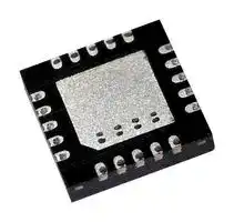
- 20-Pin QFN package
- Ultra low power shutdown mode
- Digital RSSI
- Low BOM
## **Applications**
- Remote control
- Remote meter reading
- Home security & alarm
- Remote keyless entry
- Telemetry
- Personal data logging Toy control Tire pressure monitoring Wireless PC peripherals
- Home automation
- Industrial control
- Sensor networks
- Health monitors
- Tag readers
## **Description**
Silicon Laboratories’ Si4430/31/32 devices are highly integrated, single chip wireless ISM transceivers. The high-performance EZRadioPRO[®] family includes a complete line of transmitters, receivers, and transceivers allowing the RF system designer to choose the optimal wireless part for their application.
**Ordering Information:** See page 67.
## ~~po~~ **Pin Assignments**
**==> picture [144 x 153] intentionally omitted <==**
**----- Start of picture text -----**<br>
Si4430/31/32<br>VDD_RF OUUUUo 1 20 19 18 17 16<br>TX |_| 2 || 15 SCLK<br>RXp |_| 3 GND || 14 SDI<br>RXn |_| 4 PAD || 13 SDO<br>NC |_| 5 || 12 VDD_DIG<br>KEE 6 7 8 9 10 11 NC<br>SDN XIN XOUT nIRQ nSEL<br>ANT GPIO_0 GPIO_1 GPIO_2 VR_DIG<br>**----- End of picture text -----**<br>
Patents pending
The Si4430/31/32’s high level of integration offers reduced BOM cost while simplifying the overall system design. The extremely low receive sensitivity (–121 dBm) coupled with industry leading +20 dBm output power ensures extended range and improved link performance. Built-in antenna diversity and support for frequency hopping can be used to further extend range and enhance performance.
The Si4430/31/32 offers advanced radio features including continuous frequency coverage from 240–960 MHz in 156 Hz or 312 Hz steps allowing precise tuning control. Additional system features such as an automatic wake-up timer, low battery detector, 64 byte TX/RX FIFOs, automatic packet handling, and preamble detection reduce overall current consumption and allow the use of lower-cost system MCUs. An integrated temperature sensor, general purpose ADC, poweron-reset (POR), and GPIOs further reduce overall system cost and size.
The Si4430/31/32’s digital receive architecture features a high-performance ADC and DSP based modem which performs demodulation, filtering, and packet handling for increased flexibility and performance. The direct digital transmit modulation and automatic PA power ramping ensure precise transmit modulation and reduced spectral spreading ensuring compliance with global regulations including FCC, ETSI, ARIB, and 802.15.4d regulations.
An easy-to-use calculator is provided to quickly configure the radio settings, simplifying customer's system design and reducing time to market.
**Copyright © 2010 by Silicon Laboratories**
**Si4430/31/32**
**Rev 1.1 10/10**
**- Si4430/31/32 B1**
## **Functional Block Diagram**
**Rev 1.1**
**2**
**Si4430/31/32-B1**
## **TABLE OF C ONTENTS**
|**Section**<br>**1. Electrical Specifications . . . . . . . . . . . . . . . . . . . . . . . . . . . . . . . . . . . . . . . . . . . . . .**<br>1.1. Definition of Test Conditions . . . . . . . . . . . . . . . . . . . . . . . . . . . . . . . . . . . . . . .<br>**2. Functional Description . . . . . . . . . . . . . . . . . . . . . . . . . . . . . . . . . . . . . . . . . . . . . . .**<br>2.1. Operating Modes . . . . . . . . . . . . . . . . . . . . . . . . . . . . . . . . . . . . . . . . . . . . . . . .<br>**3. Controller Interface . . . . . . . . . . . . . . . . . . . . . . . . . . . . . . . . . . . . . . . . . . . . . . . . . .**<br>3.1. Serial Peripheral Interface (SPI) . . . . . . . . . . . . . . . . . . . . . . . . . . . . . . . . . . . .<br>3.2. Operating Mode Control . . . . . . . . . . . . . . . . . . . . . . . . . . . . . . . . . . . . . . . . . .<br>3.3. Interrupts . . . . . . . . . . . . . . . . . . . . . . . . . . . . . . . . . . . . . . . . . . . . . . . . . . . . .<br>3.4. System Timing . . . . . . . . . . . . . . . . . . . . . . . . . . . . . . . . . . . . . . . . . . . . . . . . .<br>3.5. Frequency Control . . . . . . . . . . . . . . . . . . . . . . . . . . . . . . . . . . . . . . . . . . . . . . .<br>**4. Modulation Options . . . . . . . . . . . . . . . . . . . . . . . . . . . . . . . . . . . . . . . . . . . . . . . . . .**<br>4.1. Modulation Type . . . . . . . . . . . . . . . . . . . . . . . . . . . . . . . . . . . . . . . . . . . . . . . .<br>4.2. Modulation Data Source . . . . . . . . . . . . . . . . . . . . . . . . . . . . . . . . . . . . . . . . . .<br>**5. Internal Functional Blocks . . . . . . . . . . . . . . . . . . . . . . . . . . . . . . . . . . . . . . . . . . . .**<br>5.1. RX LNA . . . . . . . . . . . . . . . . . . . . . . . . . . . . . . . . . . . . . . . . . . . . . . . . . . . . . . .<br>5.2. RX I-Q Mixer . . . . . . . . . . . . . . . . . . . . . . . . . . . . . . . . . . . . . . . . . . . . . . . . . . .<br>5.3. Programmable Gain Amplifier . . . . . . . . . . . . . . . . . . . . . . . . . . . . . . . . . . . . . .<br>5.4. ADC . . . . . . . . . . . . . . . . . . . . . . . . . . . . . . . . . . . . . . . . . . . . . . . . . . . . . . . . . .<br>5.5. Digital Modem . . . . . . . . . . . . . . . . . . . . . . . . . . . . . . . . . . . . . . . . . . . . . . . . . .<br>5.6. Synthesizer . . . . . . . . . . . . . . . . . . . . . . . . . . . . . . . . . . . . . . . . . . . . . . . . . . . .<br>5.7. Power Amplifier . . . . . . . . . . . . . . . . . . . . . . . . . . . . . . . . . . . . . . . . . . . . . . . . .<br>5.8. Crystal Oscillator . . . . . . . . . . . . . . . . . . . . . . . . . . . . . . . . . . . . . . . . . . . . . . . .<br>5.9. Regulators . . . . . . . . . . . . . . . . . . . . . . . . . . . . . . . . . . . . . . . . . . . . . . . . . . . . .<br>**6. Data Handling and Packet Handler . . . . . . . . . . . . . . . . . . . . . . . . . . . . . . . . . . . . . .**<br>6.1. RX and TX FIFOs . . . . . . . . . . . . . . . . . . . . . . . . . . . . . . . . . . . . . . . . . . . . . . .<br>6.2. Packet Configuration . . . . . . . . . . . . . . . . . . . . . . . . . . . . . . . . . . . . . . . . . . . . .<br>6.3. Packet Handler TX Mode . . . . . . . . . . . . . . . . . . . . . . . . . . . . . . . . . . . . . . . . .<br>6.4. Packet Handler RX Mode . . . . . . . . . . . . . . . . . . . . . . . . . . . . . . . . . . . . . . . . .<br>6.5. Data Whitening, Manchester Encoding, and CRC . . . . . . . . . . . . . . . . . . . . . .<br>6.6. Preamble Detector . . . . . . . . . . . . . . . . . . . . . . . . . . . . . . . . . . . . . . . . . . . . . .<br>6.7. Preamble Length . . . . . . . . . . . . . . . . . . . . . . . . . . . . . . . . . . . . . . . . . . . . . . . .<br>6.8. Invalid Preamble Detector . . . . . . . . . . . . . . . . . . . . . . . . . . . . . . . . . . . . . . . . .<br>6.9. Synchronization Word Configuration . . . . . . . . . . . . . . . . . . . . . . . . . . . . . . . . .<br>6.10. Receive Header Check . . . . . . . . . . . . . . . . . . . . . . . . . . . . . . . . . . . . . . . . . .<br>6.11. TX Retransmission and Auto TX . . . . . . . . . . . . . . . . . . . . . . . . . . . . . . . . . . .<br>**7. RX Modem Configuration . . . . . . . . . . . . . . . . . . . . . . . . . . . . . . . . . . . . . . . . . . . . .**<br>7.1. Modem Settings for FSK and GFSK . . . . . . . . . . . . . . . . . . . . . . . . . . . . . . . . .<br>**8. Auxiliary Functions . . . . . . . . . . . . . . . . . . . . . . . . . . . . . . . . . . . . . . . . . . . . . . . . . .**<br>8.1. Smart Reset . . . . . . . . . . . . . . . . . . . . . . . . . . . . . . . . . . . . . . . . . . . . . . . . . . .|**Page**<br>**. . . . .7**<br>. . . .14<br>**. . . .15**<br>. . . .17<br>**. . . .18**<br>. . . .18<br>. . . .20<br>. . . .23<br>. . . .24<br>. . . .25<br>**. . . .32**<br>. . . .32<br>. . . .33<br>**. . . .37**<br>. . . .37<br>. . . .37<br>. . . .37<br>. . . .37<br>. . . .37<br>. . . .38<br>. . . .39<br>. . . .40<br>. . . .40<br>**. . . .41**<br>. . . .41<br>. . . .42<br>. . . .43<br>. . . .43<br>. . . .46<br>. . . .46<br>. . . .47<br>. . . .47<br>. . . .47<br>. . . .48<br>. . . .48<br>**. . . .49**<br>. . . .49<br>**. . . .50**<br>. . . .50|
|---|---|
**==> picture [72 x 54] intentionally omitted <==**
**Rev 1.1**
**3**
## **- Si4430/31/32 B1**
8.2. Microcontroller Clock . . . . . . . . . . . . . . . . . . . . . . . . . . . . . . . . . . . . . . . . . . . . . . . . .51 8.3. General Purpose ADC . . . . . . . . . . . . . . . . . . . . . . . . . . . . . . . . . . . . . . . . . . . . . . .52 8.4. Temperature Sensor . . . . . . . . . . . . . . . . . . . . . . . . . . . . . . . . . . . . . . . . . . . . . . . . .53 8.5. Low Battery Detector . . . . . . . . . . . . . . . . . . . . . . . . . . . . . . . . . . . . . . . . . . . . . . . . .55 8.6. Wake-Up Timer and 32 kHz Clock Source . . . . . . . . . . . . . . . . . . . . . . . . . . . . . . . .56 8.7. Low Duty Cycle Mode . . . . . . . . . . . . . . . . . . . . . . . . . . . . . . . . . . . . . . . . . . . . . . . .58 8.8. GPIO Configuration . . . . . . . . . . . . . . . . . . . . . . . . . . . . . . . . . . . . . . . . . . . . . . . . . .59 8.9. Antenna Diversity . . . . . . . . . . . . . . . . . . . . . . . . . . . . . . . . . . . . . . . . . . . . . . . . . . .60 8.10. RSSI and Clear Channel Assessment . . . . . . . . . . . . . . . . . . . . . . . . . . . . . . . . . .61 **9. Reference Design . . . . . . . . . . . . . . . . . . . . . . . . . . . . . . . . . . . . . . . . . . . . . . . . . . . . . . . .62 10. Application Notes and Reference Designs . . . . . . . . . . . . . . . . . . . . . . . . . . . . . . . . . .63 11. Customer Support . . . . . . . . . . . . . . . . . . . . . . . . . . . . . . . . . . . . . . . . . . . . . . . . . . . . . .63 12. Register Table and Descriptions . . . . . . . . . . . . . . . . . . . . . . . . . . . . . . . . . . . . . . . . . .64 13. Pin Descriptions: Si4430/31/32 . . . . . . . . . . . . . . . . . . . . . . . . . . . . . . . . . . . . . . . . . . . .66 14. Ordering Information . . . . . . . . . . . . . . . . . . . . . . . . . . . . . . . . . . . . . . . . . . . . . . . . . . . .67 15. Package Markings (Top Marks) . . . . . . . . . . . . . . . . . . . . . . . . . . . . . . . . . . . . . . . . . . . .68** 15.1. Si4430/31/32 Top Mark . . . . . . . . . . . . . . . . . . . . . . . . . . . . . . . . . . . . . . . . . . . . . .68 15.2. Top Mark Explanation . . . . . . . . . . . . . . . . . . . . . . . . . . . . . . . . . . . . . . . . . . . . . . .68 **16. Package Outline: Si4430/31/32 . . . . . . . . . . . . . . . . . . . . . . . . . . . . . . . . . . . . . . . . . . . .69 17. PCB Land Pattern: Si4430/31/32 . . . . . . . . . . . . . . . . . . . . . . . . . . . . . . . . . . . . . . . . . . .70 Document Change List . . . . . . . . . . . . . . . . . . . . . . . . . . . . . . . . . . . . . . . . . . . . . . . . . . . . .72 Contact Information . . . . . . . . . . . . . . . . . . . . . . . . . . . . . . . . . . . . . . . . . . . . . . . . . . . . . . . .74**
**==> picture [72 x 54] intentionally omitted <==**
**Rev 1.1**
**4**
**Si4430/31/32-B1**
## **L IST OF F IGURES**
Figure 1. Si4430/31 RX/TX Direct-Tie Application Example .....................................................16 Figure 2. Si4432 Antenna Diversity Application Example .........................................................16 Figure 3. SPI Timing..................................................................................................................18 Figure 4. SPI Timing—READ Mode..........................................................................................19 Figure 5. SPI Timing—Burst Write Mode ..................................................................................19 Figure 6. SPI Timing—Burst Read Mode..................................................................................19 Figure 7. State Machine Diagram..............................................................................................20 Figure 8. TX Timing...................................................................................................................24 Figure 9. RX Timing ..................................................................................................................24 Figure 10. Frequency Deviation ................................................................................................28 Figure 11. Sensitivity at 1% PER vs. Carrier Frequency Offset ................................................29 Figure 12. FSK vs GFSK Spectrums.........................................................................................32 Figure 13. Direct Synchronous Mode Example.........................................................................35 Figure 14. Direct Asynchronous Mode Example.......................................................................35 Figure 15. Microcontroller Connections.....................................................................................36 Figure 16. PLL Synthesizer Block Diagram...............................................................................38 Figure 17. FIFO Thresholds ......................................................................................................41 Figure 18. Packet Structure.......................................................................................................42 Figure 19. Multiple Packets in TX Packet Handler....................................................................43 Figure 20. Required RX Packet Structure with Packet Handler Disabled.................................43 Figure 21. Multiple Packets in RX Packet Handler....................................................................43 Figure 22. Multiple Packets in RX with CRC or Header Error...................................................44 Figure 23. Operation of Data Whitening, Manchester Encoding, and CRC ..............................46 Figure 24. Manchester Coding Example...................................................................................46 Figure 25. Header .....................................................................................................................48 Figure 26. POR Glitch Parameters............................................................................................50 Figure 27. General Purpose ADC Architecture .........................................................................52 Figure 28. Temperature Ranges using ADC8...........................................................................54 Figure 29. WUT Interrupt and WUT Operation..........................................................................57 Figure 30. Low Duty Cycle Mode ..............................................................................................58 Figure 31. RSSI Value vs. Input Power.....................................................................................61 Figure 32. TX/RX Direct-Tie Reference Design—Schematic....................................................62 Figure 33. 20-Pin Quad Flat No-Lead (QFN) ............................................................................69 Figure 34. PCB Land Pattern ....................................................................................................70
**==> picture [72 x 54] intentionally omitted <==**
**Rev 1.1**
**5**
**Si4430/31/32-B1**
## **L IST OF TABLES**
Table 1. DC Characteristics[1 ] ......................................................................................................7 Table 2. Synthesizer AC Electrical Characteristics[1 ] ...................................................................8 Table 3. Receiver AC Electrical Characteristics[1] .......................................................................9 Table 4. Transmitter AC Electrical Characteristics[1 ] .................................................................10 Table 5. Auxiliary Block Specifications[1 ] ...................................................................................11 Table 6. Digital IO Specifications (SDO, SDI, SCLK, nSEL, and nIRQ) ...................................12 Table 7. GPIO Specifications (GPIO_0, GPIO_1, and GPIO_2) ..............................................12 Table 8. Absolute Maximum Ratings ........................................................................................13 Table 9. Operating Modes ........................................................................................................17 Table 10. Serial Interface Timing Parameters ..........................................................................18 Table 11. Operating Modes Response Time ............................................................................20 Table 12. Frequency Band Selection .......................................................................................26 Table 13. Packet Handler Registers .........................................................................................45 Table 14. Minimum Receiver Settling Time ..............................................................................47 Table 15. POR Parameters ......................................................................................................50 Table 16. Temperature Sensor Range .....................................................................................53 Table 17. Antenna Diversity Control .........................................................................................60 Table 18. Register Descriptions ...............................................................................................64 Table 19. Package Dimensions ................................................................................................69 Table 20. PCB Land Pattern Dimensions .................................................................................71
**==> picture [72 x 54] intentionally omitted <==**
**Rev 1.1**
**6**
**- Si4430/31/32 B1**
## **1. Electrical Specifications**
## **Table 1. DC Characteristics[1]**
|**Parameter**|**Symbol**|**Conditions**|**Min**|**Typ**|**Max**|**Units**|
|---|---|---|---|---|---|---|
|Supply Voltage Range|VDD||1.8|3.0|3.6|V|
|Power Saving Modes|IShutdown|RC Oscillator, Main Digital Regulator,<br>and Low Power Digital Regulator OFF2|—|15|50|nA|
||IStandby|Low Power Digital Regulator ON (Register values retained)<br>and Main Digital Regulator, and RC Oscillator OFF|—|450|800|nA|
||ISleep|RC Oscillator and Low Power Digital Regulator ON<br>(Register values retained) and Main Digital Regulator OFF|—|1|—|µA|
||ISensor-LBD|Main Digital Regulator and Low Battery Detector ON,<br>Crystal Oscillator and all other blocks OFF2|—|1|—|µA|
||ISensor-TS|Main Digital Regulator and Temperature Sensor ON,<br>Crystal Oscillator and all other blocks OFF2|—|1|—|µA|
||IReady|Crystal Oscillator and Main Digital Regulator ON,<br>all other blocks OFF. Crystal Oscillator buffer disabled|—|800|—|µA|
|TUNE Mode Current|ITune|Synthesizer and regulators enabled|—|8.5|—|mA|
|RX Mode Current|IRX||—|18.5|—|mA|
|TX Mode Current<br>—Si4432|ITX_+20|txpow[2:0] = 111 (+20 dBm)<br>Using Silicon Labs’ Reference Design. TX current<br>consumption is dependent on match and board layout.|—|85|—|mA|
|TX Mode Current<br>—Si4430/31|ITX_+13|txpow[2:0] = 110 (+13 dBm)<br>Using Silicon Labs’ Reference Design. TX current<br>consumption is dependent on match and board layout.|—|30|—|mA|
||ITX_+1|txpow[2:0] = 010 (+1 dBm)<br>Using Silicon Labs’ Reference Design. TX current<br>consumption is dependent on match and board layout.|—|17|—|mA|
|**Notes:**<br>**1.** All specification guaranteed by production test unless otherwise noted. Production test conditions and max limits are<br>listed in the "Production Test Conditions" section on page 14.<br>**2.**Guaranteed by qualification. Qualification test conditions are listed in the "Production Test Conditions" section on<br>page 14.|||||||
## **Notes:**
**1.** All specification guaranteed by production test unless otherwise noted. Production test conditions and max limits are listed in the "Production Test Conditions" section on page 14.
**2.** Guaranteed by qualification. Qualification test conditions are listed in the "Production Test Conditions" section on page 14.
**==> picture [72 x 54] intentionally omitted <==**
**Rev 1.1**
**7**
**- Si4430/31/32 B1**
**Table 2. Synthesizer AC Electrical Characteristics[1]**
|**Parameter**|**Symbol**|**Conditions**|**Min**|**Typ**|**Max**|**Units**|
|---|---|---|---|---|---|---|
|Synthesizer Frequency<br>Range—Si4431/32|FSYN||240|—|930|MHz|
|Synthesizer Frequency<br>Range—Si4430|FSYN||900|—|960|MHz|
|Synthesizer Frequency<br>Resolution2|FRES-LB|Low Band, 240–480 MHz|—|156.25|—|Hz|
||FRES-HB|High Band, 480–960 MHz|—|312.5|—|Hz|
|Reference Frequency<br>Input Level2|fREF_LV|When using external reference signal<br>driving XOUT pin, instead of using<br>crystal. Measured peak-to-peak (VPP)|0.7|—|1.6|V|
|Synthesizer Settling Time2|tLOCK|Measured from exiting Ready mode with<br>XOSC running to any frequency.<br>Including VCO Calibration.|—|200|—|µs|
|Residual FM2|FRMS|Integrated over250 kHz bandwidth<br>(500 Hz lower bound of integration)|—|2|4|kHzRMS|
|Phase Noise2|L(fM)|F = 10 kHz|—|–80|—|dBc/Hz|
|||F = 100 kHz|—|–90|—|dBc/Hz|
|||F = 1 MHz|—|–115|—|dBc/Hz|
|||F = 10 MHz|—|–130|—|dBc/Hz|
|**Notes:**<br>**1.** All specification guaranteed by production test unless otherwise noted. Production test conditions and max limits are<br>listed in the "Production Test Conditions" section on page 14.<br>**2.**Guaranteed by qualification. Qualification test conditions are listed in the "Production Test Conditions" section on<br>page 14.|||||||
## **Notes:**
**1.** All specification guaranteed by production test unless otherwise noted. Production test conditions and max limits are listed in the "Production Test Conditions" section on page 14.
**2.** Guaranteed by qualification. Qualification test conditions are listed in the "Production Test Conditions" section on page 14.
**==> picture [72 x 54] intentionally omitted <==**
**Rev 1.1**
**8**
**- Si4430/31/32 B1**
## **Table 3. Receiver AC Electrical Characteristics[1]**
|**Parameter**|**Symbol**|**Conditions**|**Min**|**Typ**|**Max**|**Units**|
|---|---|---|---|---|---|---|
|RX Frequency<br>Range—Si4431/32|FRX||240|—|930|MHz|
|RX Frequency<br>Range—Si4430|FRX||900|—|960|MHz|
|RX Sensitivity2|PRX_2|(BER < 0.1%)<br>(2 kbps, GFSK, BT = 0.5,<br>f =5 kHz)3|—|–121|—|dBm|
||PRX_40|(BER < 0.1%)<br>(40 kbps, GFSK, BT = 0.5,<br>f =20 kHz)3|—|–108|—|dBm|
||PRX_100|(BER < 0.1%)<br>(100 kbps, GFSK, BT = 0.5,<br>f =50 kHz)3|—|–104|—|dBm|
||PRX_125|(BER < 0.1%)<br>(125 kbps, GFSK, BT = 0.5,<br>f =62.5 kHz)|—|–101|—|dBm|
||PRX_OOK|(BER < 0.1%)<br>(4.8 kbps,350 kHz BW,OOK)3|—|–110|—|dBm|
|||(BER < 0.1%)<br>(40 kbps,400 kHz BW,OOK)3|—|–102|—|dBm|
|RX Channel Bandwidth3|BW||2.6|—|620|kHz|
|BER Variation vs Power<br>Level3|PRX_RES|Up to +5 dBm Input Level|—|0|0.1|ppm|
|LNA Input Impedance3<br>(Unmatched—measured<br>differentially across RX<br>input pins)|RIN-RX|915 MHz|—|51–60j|—||
|||868 MHz|—|54–63j|—||
|||433 MHz|—|89–110j|—||
|||315 MHz|—|107–137j|—||
|RSSI Resolution|RESRSSI||—|±0.5|—|dB|
|1-Ch Offset Selectivity3|C/I1-CH|Desired Ref Signal 3 dB above sensitivity,<br>BER < 0.1%. Interferer and desired modu-<br>lated with 40 kbpsF = 20 kHz GFSK with<br>BT = 0.5,channel spacing= 150 kHz|—|–31|—|dB|
|2-Ch Offset Selectivity3|C/I2-CH||<br>—|–35|—|dB|
| 3-Ch Offset Selectivity3|C/I3-CH||<br>—|–40|—|dB|
|Blocking at 1 MHz Offset3|1MBLOCK|Desired Ref Signal 3 dB above sensitivity.<br>Interferer and desired modulated with<br>40 kbpsF = 20 kHz GFSK with BT = 0.5|—|–52|—|dB|
|Blocking at 4 MHz Offset3|4MBLOCK||—|–56|—|dB|
|Blocking at 8 MHz Offset3|8MBLOCK||—|–63|—|dB|
|Image Rejection3|ImREJ|Rejection at the image frequency.<br>IF=937 kHz|—|–30|—|dB|
|Spurious Emissions3|POB_RX1|Measured at RX pins|—|—|–54|dBm|
|**Notes:**<br>**1.** All specification guaranteed by production test unless otherwise noted. Production test conditions and max limits are listed<br>in the "Production Test Conditions" section on page 14.<br>**2.**Receive sensitivity at multiples of 30 MHz may be degraded. If channels with a multiple of 30 MHz are required it is<br>recommended to shift the crystal frequency. Contact Silicon Labs Applications Support for recommendations.<br>**3.**Guaranteed by qualification. Qualification test conditions are listed in the "Production Test Conditions" section on page 14.|||||||
## **Notes:**
**1.** All specification guaranteed by production test unless otherwise noted. Production test conditions and max limits are listed in the "Production Test Conditions" section on page 14.
**2.** Receive sensitivity at multiples of 30 MHz may be degraded. If channels with a multiple of 30 MHz are required it is recommended to shift the crystal frequency. Contact Silicon Labs Applications Support for recommendations.
**3.** Guaranteed by qualification. Qualification test conditions are listed in the "Production Test Conditions" section on page 14.
**==> picture [72 x 54] intentionally omitted <==**
**Rev 1.1**
**9**
**- Si4430/31/32 B1**
## **Table 4. Transmitter AC Electrical Characteristics[1]**
|**Parameter**|**Symbol**|**Conditions**|**Min**|**Typ**|**Max**|**Units**|
|---|---|---|---|---|---|---|
|TX Frequency<br>Range—Si4431/32|FTX||240|—|930|MHz|
|TX Frequency<br>Range—Si4430|FTX||900|—|960|MHz|
|FSK Data Rate2|DRFSK||0.123|—|256|kbps|
|OOK Data Rate2|DROOK||0.123|—|40|kbps|
|Modulation Deviation|∆f1|860–960 MHz|±0.625||±320|kHz|
||∆f2|240–860 MHz|±0.625||±160|kHz|
|Modulation Deviation<br>Resolution2|∆fRES||—|0.625|—|kHz|
|Output Power<br>Range—Si44323|PTX||+1|—|+20|dBm|
|Output Power<br>Range—Si4430/313|PTX||–8|—|+13|dBm|
|TX RF Output Steps2|PRF_OUT|controlled by txpow[2:0]|—|3|—|dB|
|TX RF Output Level2<br>Variation vs. Temperature|PRF_TEMP|–40 to +85C|—|2|—|dB|
|TX RF Output Level<br>Variation vs. Frequency2|PRF_FREQ|Measured across any one<br>frequency band|—|1|—|dB|
|Transmit Modulation<br>Filtering2|B*T|Gaussian Filtering Bandwith Time<br>Product|—|0.5|—||
|Spurious Emissions2|POB-TX1|POUT= +13 dBm,<br>Frequencies <1 GHz|—|—|–54|dBm|
||POB-TX2|1–12.75 GHz, excluding harmonics|—|—|–54|dBm|
|Harmonics2|P2HARM|Using reference design TX matching<br>network and filter with max output<br>power. Harmonics reduce linearly with<br>output power.|—|—|–42|dBm|
||P3HARM||—|—|–42|dBm|
|**Notes:**<br>**1.** All specification guaranteed by production test unless otherwise noted. Production test conditions and max limits are<br>listed in the "Production Test Conditions" section on page 14.<br>**2.**Guaranteed by qualification. Qualification test conditions are listed in the "Production Test Conditions" section on<br>page 14.<br>**3.**Output power is dependent on matching components, board layout, and is measured at the pin.|||||||
## **Notes:**
**1.** All specification guaranteed by production test unless otherwise noted. Production test conditions and max limits are listed in the "Production Test Conditions" section on page 14.
**2.** Guaranteed by qualification. Qualification test conditions are listed in the "Production Test Conditions" section on page 14.
**3.** Output power is dependent on matching components, board layout, and is measured at the pin.
**==> picture [72 x 54] intentionally omitted <==**
**Rev 1.1**
**10**
**- Si4430/31/32 B1**
## **Table 5. Auxiliary Block Specifications[1]**
|**Parameter**|**Symbol**|**Conditions**|**Min**|**Typ**|**Max**|**Units**|
|---|---|---|---|---|---|---|
|Temperature Sensor<br>Accuracy2|TSA|After calibrated via sensor offset<br>register tvoffs[7:0]|—|0.5|—|°C|
|Temperature Sensor<br>Sensitivity2|TSS||—|5|—|mV/°C|
|Low Battery Detector<br>Resolution2|LBDRES||—|50|—|mV|
|Low Battery Detector<br>Conversion Time2|LBDCT||—|250|—|µs|
|Microcontroller Clock<br>Output Frequency|FMC|Configurable to 30 MHz,<br>15 MHz, 10 MHz, 4 MHz,<br>3 MHz, 2 MHz, 1 MHz, or<br>32.768 kHz|32.768K|—|30M|Hz|
|General Purpose ADC Res-<br>olution2|ADCENB||—|8|—|bit|
|General Purpose ADC Bit<br>Resolution2|ADCRES||—|4|—|mV/bit|
|Temp Sensor & General<br>Purpose ADC Conversion<br>Time2|ADCCT||—|305|—|µs|
|30 MHz XTAL Start-Up time|t30M|Using XTAL and board layout in<br>reference design. Start-up time<br>will vary with XTAL type and<br>board layout.|—|600|—|µs|
|30 MHz XTAL Cap<br>Resolution2|30MRES|See "5.8. Crystal Oscillator" on<br>page 40 for total load<br>capacitance calculation|—|97|—|fF|
|32 kHz XTAL Start-Up Time2|t32k||—|6|—|sec|
|32 kHz Accuracy using<br>Internal RC Oscillator2|32KRCRES||—|1000|—|ppm|
|32 kHz RC Oscillator Start-<br>Up|t32kRC||—|500|—|µs|
|POR Reset Time|tPOR||—|16|—|ms|
|Software Reset Time2|tsoft||—|250|—|µs|
|**Notes:**<br>**1.** All specification guaranteed by production test unless otherwise noted. Production test conditions and max limits are<br>listed in the "Production Test Conditions" section on page 14.<br>**2.**Guaranteed by qualification. Qualification test conditions are listed in the "Production Test Conditions" section on<br>page 14.|||||||
## **Notes:**
**1.** All specification guaranteed by production test unless otherwise noted. Production test conditions and max limits are listed in the "Production Test Conditions" section on page 14.
**2.** Guaranteed by qualification. Qualification test conditions are listed in the "Production Test Conditions" section on page 14.
**==> picture [72 x 54] intentionally omitted <==**
**Rev 1.1**
**11**
**- Si4430/31/32 B1**
**Table 6. Digital IO Specifications (SDO, SDI, SCLK, nSEL, and nIRQ)**
|**Parameter**|**Symbol**|**Conditions**|**Min**|**Typ**|**Max**|**Units**|
|---|---|---|---|---|---|---|
|Rise Time|TRISE|0.1 x VDDto 0.9 x VDD, CL= 5 pF|—|—|8|ns|
|Fall Time|TFALL|0.9 x VDDto 0.1 x VDD,CL= 5 pF|—|—|8|ns|
|Input Capacitance|CIN||—|—|1|pF|
|Logic High Level Input Voltage|VIH||VDD– 0.6|—|—|V|
|Logic Low Level Input Voltage|VIL|||—|0.6|V|
|Input Current|IIN|0<VIN< VDD|–100|—|100|nA|
|Logic High Level Output<br>Voltage|VOH|IOH<1 mA source, VDD=1.8 V|VDD– 0.6|—|—|V|
|Logic Low Level Output Voltage|VOL|IOL<1 mA sink, VDD=1.8 V|—|—|0.6|V|
|**Note:** All specifications guaranteed by qualification. Qualification test conditions are listed in the "Production Test Conditions"<br>section on page 14.|||||||
**Note:** All specifications guaranteed by qualification. Qualification test conditions are listed in the "Production Test Conditions" section on page 14.
**Table 7. GPIO Specifications (GPIO_0, GPIO_1, and GPIO_2)**
|**Parameter**|**Symbol**|**Conditions**|**Min**|**Typ**|**Max**|**Units**|
|---|---|---|---|---|---|---|
|Rise Time|TRISE|0.1 x VDDto 0.9 x VDD,<br>CL= 10 pF, DRV<1:0>=HH|—|—|8|ns|
|Fall Time|TFALL|0.9 x VDDto 0.1 x VDD,<br>CL= 10 pF, DRV<1:0>=HH|—|—|8|ns|
|Input Capacitance|CIN||—|—|1|pF|
|Logic High Level Input Voltage|VIH||VDD– 0.6|—||V|
|Logic Low Level Input Voltage|VIL||—|—|0.6|V|
|Input Current|IIN|0<VIN< VDD|–100|—|100|nA|
|Input Current If Pullup is Activated|IINP|VIL=0 V|5|—|25|µA|
|Maximum Output Current|IOmaxLL|DRV<1:0>=LL|0.1|0.5|0.8|mA|
||IOmaxLH|DRV<1:0>=LH|0.9|2.3|3.5|mA|
||IOmaxHL|DRV<1:0>=HL|1.5|3.1|4.8|mA|
||IOmaxHH|DRV<1:0>=HH|1.8|3.6|5.4|mA|
|Logic High Level Output Voltage|VOH|IOH< IOmaxsource,<br>VDD=1.8 V|VDD– 0.6|—|—|V|
|Logic Low Level Output Voltage|VOL|IOL< IOmaxsink,<br>VDD=1.8 V|—|—|0.6|V|
|**Note:** All specifications guaranteed by qualification. Qualification test conditions are listed in the "Production Test Conditions"<br>section on page 14.|||||||
**Note:** All specifications guaranteed by qualification. Qualification test conditions are listed in the "Production Test Conditions" section on page 14.
**==> picture [72 x 54] intentionally omitted <==**
**Rev 1.1**
**12**
**- Si4430/31/32 B1**
## **Table 8. Absolute Maximum Ratings**
|**Table 8. Absolute Maximum Ratings**|||
|---|---|---|
|**Parameter**|**Value**|**Unit**|
|VDDto GND|–0.3, +3.6|V|
|Instantaneous VRF-peakto GND on TX Output Pin|–0.3, +8.0|V|
|Sustained VRF-peakto GND on TX Output Pin|–0.3, +6.5|V|
|Voltage on Digital Control Inputs|–0.3, VDD+ 0.3|V|
|Voltage on Analog Inputs|–0.3, VDD+ 0.3|V|
|RX Input Power|+10|dBm|
|Operating Ambient Temperature Range TA|–40 to +85|C|
|Thermal Impedance JA|30|C/W|
|Junction Temperature TJ|+125|C|
|Storage Temperature Range TSTG|–55 to +125|C|
|**Note:** Stresses beyond those listed under “Absolute Maximum Ratings” may cause permanent damage to the device. These<br>are stress ratings only and functional operation of the device at or beyond these ratings in the operational sections of<br>the specifications is not implied. Exposure to absolute maximum rating conditions for extended periods may affect<br>device reliability. Power Amplifier may be damaged if switched on without proper load or termination connected. TX<br>matching network design will influence TX VRF-peakon TX output pin. Caution: ESD sensitive device.|||
**Note:** Stresses beyond those listed under “Absolute Maximum Ratings” may cause permanent damage to the device. These are stress ratings only and functional operation of the device at or beyond these ratings in the operational sections of the specifications is not implied. Exposure to absolute maximum rating conditions for extended periods may affect device reliability. Power Amplifier may be damaged if switched on without proper load or termination connected. TX matching network design will influence TX VRF-peak on TX output pin. Caution: ESD sensitive device.
**==> picture [72 x 54] intentionally omitted <==**
**Rev 1.1**
**13**
**- Si4430/31/32 B1**
## **1.1. Definition of Test Conditions**
## **Production Test Conditions:**
- TA = +25 °C
- VDD = +3.3 VDC
- Sensitivity measured at 919 MHz
- TX output power measured at 915 MHz
- External reference signal (XOUT) = 1.0 VPP at 30 MHz, centered around 0.8 VDC
- Production test schematic (unless noted otherwise)
- All RF input and output levels referred to the pins of the Si4430/31/32 (not the RF module)
## **Qualification Test Conditions:**
- TA = –40 to +85 °C
- VDD = +1.8 to +3.6 VDC
- Using TX/RX Split Antenna reference design or production test schematic
- All RF input and output levels referred to the pins of the Si4430/31/32 (not the RF module)
**==> picture [72 x 54] intentionally omitted <==**
**Rev 1.1**
**14**
**- Si4430/31/32 B1**
## **2. Functional Description**
The Si4430/31/32 are ISM wireless transceivers with continuous frequency tuning over their specified bands which encompasses from 240–960 MHz. The wide operating voltage range of 1.8–3.6 V and low current consumption makes the Si4430/31/32 an ideal solution for battery powered applications.
The Si4430/31/32 operates as a time division duplexing (TDD) transceiver where the device alternately transmits and receives data packets. The device uses a single-conversion mixer to downconvert the 2-level FSK/GFSK/OOK modulated receive signal to a low IF frequency. Following a programmable gain amplifier (PGA) the signal is converted to the digital domain by a high performance ADC allowing filtering, demodulation, slicing, and packet handling to be performed in the built-in DSP increasing the receiver’s performance and flexibility versus analog based architectures. The demodulated signal is then output to the system MCU through a programmable GPIO or via the standard SPI bus by reading the 64-byte RX FIFO.
A single high precision local oscillator (LO) is used for both transmit and receive modes since the transmitter and receiver do not operate at the same time. The LO is generated by an integrated VCO and Fractional-N PLL synthesizer. The synthesizer is designed to support configurable data rates, output frequency and frequency deviation at any frequency between 240–960 MHz. The transmit FSK data is modulated directly into the data stream and can be shaped by a Gaussian low-pass filter to reduce unwanted spectral content.
The Si4432’s PA output power can be configured between +1 and +20 dBm in 3 dB steps, while the Si4430/31's PA output power can be configured between –8 and +13 dBm in 3 dB steps. The PA is single-ended to allow for easy antenna matching and low BOM cost. The PA incorporates automatic ramp-up and rampdown control to reduce unwanted spectral spreading. The +20 dBm power amplifier of the Si4432 can also be used to compensate for the reduced performance of a lower cost, lower performance antenna or antenna with size constraints due to a small form-factor. Competing solutions require large and expensive external PAs to achieve comparable performance. The Si4430/31/32 supports frequency hopping, TX/RX switch control, and antenna diversity switch control to extend the link range and improve performance.
The Si4430/31/32 is designed to work with a microcontroller, crystal, and a few external components to create a very low cost system as shown Figure 1. Voltage regulators are integrated on-chip which allows for a wide operating supply voltage range from +1.8 to +3.6 V. A standard 4-pin SPI bus is used to communicate with an external microcontroller. Three configurable general purpose I/Os are available. A complete list of the available GPIO functions is shown in "8. Auxiliary Functions" on page 50 and includes microcontroller clock output, Antenna Diversity, POR, and various interrupts.
The application shown in Figure 1 is designed for a system with a TX/RX direct-tie configuration without the use of a TX/RX switch. Most lower power applications will use this configuration. A complete direct-tie reference design is available from Silicon Laboratories applications support.
For applications seeking improved performance in the presence of multipath fading antenna diversity can be used. Antenna diversity support is integrated into the Si4430/31/32 and can improve the system link budget by 8–10 dB in the presence of these fading conditions, resulting in substantial range increases. A complete Antenna Diversity reference design is available from Silicon Laboratories applications support.
**==> picture [72 x 54] intentionally omitted <==**
**Rev 1.1**
**15**
**- Si4430/31/32 B1**
**==> picture [408 x 295] intentionally omitted <==**
**----- Start of picture text -----**<br>
supply voltage<br>C6 C7 C8 X1 VDD<br>30MHz GP1<br>100p 100n 1u<br>GP2<br>L1 VDD_RF 1 15 SCLK GP3<br>L2 TX SDI GP4<br>2 14<br>L4 L3 C1 RFp 3 Si4430/31 13 SDO GP5 microcontroller<br>C3 C2 RXn VDD_D<br>4 12<br>C4 NC 5 11 NC<br>L6 L5<br>C9<br>1u<br>C5<br>VSS<br>Programmable load capacitors for X1 are integrated.<br>L1-L6 and C1-C5 values depend on frequency band, antenna<br>impedance, output power and supply voltage range.<br>SDN XIN XOUT nIRQ nSEL<br>20 19 18 17 16<br>6 7 8 9 10<br>ANT GPIO0 GPIO1 GPIO2 VR_DIG<br>**----- End of picture text -----**<br>
**Figure 1. Si4430/31 RX/TX Direct-Tie Application Example**
**==> picture [466 x 283] intentionally omitted <==**
**----- Start of picture text -----**<br>
Supply Voltage<br>C6 C7 C8 X1 VDD<br>30 MHz GP1<br>100 p 100 n 1 u<br>GP2<br>TR & ANT-DIV L3 L2 L1 VDD_TXRF 1 15 SDISCLK GP3GP4<br>Switch 2 14<br>1 6 C3 C2 C1 RFp 3 Si4432 13 SDO GP5 Microcontroller<br>RXn VDD_D<br>2 5 4 12<br>NC 5 11 NC<br>3 4 C4<br>L4 C9<br>1 u<br>C5<br>VSS<br>Programmable load capacitors for X1 are integrated.<br>L1–L4 and C1–C5 values depend on frequency band, antenna<br>impedance, output power, and supply voltage range.<br>SDN XIN XOUT nIRQ nSEL<br>20 19 18 17 16<br>6 7 8 9 10<br>ANT GPIO0 GPIO1 GPIO2 VR_DIG<br>**----- End of picture text -----**<br>
**Figure 2. Si4432 Antenna Diversity Application Example**
**==> picture [72 x 54] intentionally omitted <==**
**Rev 1.1**
**16**
**- Si4430/31/32 B1**
## **2.1. Operating Modes**
The Si4430/31/32 provides several operating modes which can be used to optimize the power consumption for a given application. Depending upon the system communication protocol, an optimal trade-off between the radio wake time and power consumption can be achieved.
Table 9 summarizes the operating modes of the Si4430/31/32. In general, any given operating mode may be classified as an active mode or a power saving mode. The table indicates which block(s) are enabled (active) in each corresponding mode. With the exception of the SHUTDOWN mode, all can be dynamically selected by sending the appropriate commands over the SPI. An “X” in any cell means that, in the given mode of operation, that block can be independently programmed to be either ON or OFF, without noticeably impacting the current consumption. The SPI circuit block includes the SPI interface hardware and the device register space. The 32 kHz OSC block includes the 32.768 kHz RC oscillator or 32.768 kHz crystal oscillator and wake-up timer. AUX (Auxiliary Blocks) includes the temperature sensor, general purpose ADC, and low-battery detector.
**Table 9. Operating Modes**
|**Mode**<br>**Name**||**Circuit Blocks**|**Circuit Blocks**|**Circuit Blocks**|**Circuit Blocks**|**Circuit Blocks**|**Circuit Blocks**|**Circuit Blocks**||
|---|---|---|---|---|---|---|---|---|---|
||**Digital LDO**|**SPI**|**32 kHz OSC**|**AUX**|**30 MHz**<br>**XTAL**|**PLL**|**PA**|**RX**|**IVDD**|
|SHUT-<br>DOWN|OFF (Register<br>contents lost)|OFF|OFF|OFF|OFF|OFF|OFF|OFF|15 nA|
|STANDBY|ON (Register<br>contents<br>retained)|ON|OFF|OFF|OFF|OFF|OFF|OFF|450 nA|
|SLEEP||ON|ON|X|OFF|OFF|OFF|OFF|1 µA|
|SENSOR||ON|X|ON|OFF|OFF|OFF|OFF|1 µA|
|READY||ON|X|X|ON|OFF|OFF|OFF|800 µA|
|TUNING||ON|X|X|ON|ON|OFF|OFF|8.5 mA|
|TRANSMIT||ON|X|X|ON|ON|ON|OFF|30 mA*|
|RECEIVE||ON|X|X|ON|ON|OFF|ON|18.5 mA|
|***Note:**Using Si4430/31 at +13 dBm using recommended reference design.||||||||||
***Note:** Using Si4430/31 at +13 dBm using recommended reference design.
**==> picture [72 x 54] intentionally omitted <==**
**Rev 1.1**
**17**
**- Si4430/31/32 B1**
## **3. Controller Interface**
## **3.1. Serial Peripheral Interface (SPI)**
The Si4430/31/32 communicates with the host MCU over a standard 3-wire SPI interface: SCLK, SDI, and nSEL. The host MCU can read data from the device on the SDO output pin. A SPI transaction is a 16-bit sequence which consists of a Read-Write (R/W) select bit, followed by a 7-bit address field (ADDR), and an 8-bit data field (DATA) as demonstrated in Figure 3. The 7-bit address field is used to select one of the 128, 8-bit control registers. The R/W select bit determines whether the SPI transaction is a read or write transaction. If R/W = 1 it signifies a WRITE transaction, while R/W = 0 signifies a READ transaction. The contents (ADDR or DATA) are latched into the Si4430/31/32 every eight clock cycles. The timing parameters for the SPI interface are shown in Table 10. The SCLK rate is flexible with a maximum rate of 10 MHz.
**==> picture [423 x 99] intentionally omitted <==**
**----- Start of picture text -----**<br>
Address Data<br>MSB LSB<br>SDI RW A6 A5 A4 A3 A2 A1 A0 D7 D6 D5 D4 D3 D2 D1 D0 xx xx RW A7<br>SCLK<br>nSEL<br>**----- End of picture text -----**<br>
## **Figure 3. SPI Timing**
**Table 10. Serial Interface Timing Parameters**
|**Symbol**|**Parameter**|**Min (nsec)**||||**Diagram**||
|---|---|---|---|---|---|---|---|
|tCH|Clock high time|40|SDI<br>SCLK<br>SDO<br>nSEL||||tSH<br>tDE<br>tSW|
|tCL|Clock low time|40||||tCL<br>tCH<br>tDS<br>tDH<br>tDD||
|tDS|Data setup time|20|||tSS|||
|tDH|Data hold time|20||||||
|||||||||
|tDD|Output data delay time|20||||||
|||||||||
|tEN|Output enable time|20||||||
||||||tEN|||
|tDE|Output disable time|50||||||
|tSS|Select setup time|20||||||
|tSH|Select hold time|50||||||
|tSW|Select high period|80||||||
To read back data from the Si4430/31/32, the R/W bit must be set to 0 followed by the 7-bit address of the register from which to read. The 8 bit DATA field following the 7-bit ADDR field is ignored on the SDI pin when R/W = 0. The next eight negative edge transitions of the SCLK signal will clock out the contents of the selected register. The data read from the selected register will be available on the SDO output pin. The READ function is shown in Figure 4. After the READ function is completed the SDO pin will remain at either a logic 1 or logic 0 state depending on the last data bit clocked out (D0). When nSEL goes high the SDO output pin will be pulled high by internal pullup.
**==> picture [72 x 54] intentionally omitted <==**
**Rev 1.1**
**18**
**- Si4430/31/32 B1**
**==> picture [354 x 121] intentionally omitted <==**
**----- Start of picture text -----**<br>
First Bit Last Bit<br>RW D7 D6 D5 D4 D3 D2 D1 D0<br>SDI =0 A6 A5 A4 A3 A2 A1 A0 =X =X =X =X =X =X =X =X<br>— tTTTTT<br>SCLK<br>— [S] [U] PETTITT TTT [A] tT]<br>First Bit Last Bit<br>SDO D7 D6 D5 D4 D3 D2 D1 D0<br>C E T EE ET<br>nSEL .<br>**----- End of picture text -----**<br>
**Figure 4. SPI Timing—READ Mode**
The SPI interface contains a burst read/write mode which allows for reading/writing sequential registers without having to re-send the SPI address. When the nSEL bit is held low while continuing to send SCLK pulses, the SPI interface will automatically increment the ADDR and read from/write to the next address. An example burst write transaction is illustrated in Figure 5 and a burst read in Figure 6. As long as nSEL is held low, input data will be latched into the Si4430/31/32 every eight SCLK cycles.
**First Bit Last Bit RW D7 D6 D5 D4 D3 D2 D1 D0 D7 D6 D5 D4 D3 D2 D1 D0 SDI =1 A6 A5 A4 A3 A2 A1 A0 =X =X =X =X =X =X =X =X =X =X =X =X =X =X =X =X** ~~—t~~ TTTTTLTETITT ~~Ttt~~ Titt **SCLK** ~~FUL —~~ ttt ttt t ~~i~~ **nSEL** ~~bo~~ **Figure 5. SPI Timing—Burst Write Mode First Bit Last Bit RW D7 D6 D5 D4 D3 D2 D1 D0 SDI =0 A6 A5 A4 A3 A2 A1 A0 =X =X =X =X =X =X =X =X** ~~—I~~ [TITTITITETitTi **SCLK** ~~FUE~~ — t ~~t~~ y ~~}~~ **First Bit SDO D7 D6 D5 D4 D3 D2 D1 D0 D7 D6 D5 D4 D3 D2 D1 D0** ~~ET~~ ETE ETE ET ~~E~~ ETE EE **nSEL** ~~i~~ **Figure 6. SPI Timing—Burst Read Mode**
**Rev 1.1**
**19**
**- Si4430/31/32 B1**
## **3.2. Operating Mode Control**
There are four primary states in the Si4430/31/32 radio state machine: SHUTDOWN, IDLE, TX, and RX (see Figure 7). The SHUTDOWN state completely shuts down the radio to minimize current consumption. There are five different configurations/options for the IDLE state which can be selected to optimize the chip to the applications needs. "Register 07h. Operating Mode and Function Control 1" controls which operating mode/state is selected with the exception of SHUTDOWN which is controlled by SDN pin 20. The TX and RX state may be reached automatically from any of the IDLE states by setting the txon/rxon bits in "Register 07h. Operating Mode and Function Control 1". Table 11 shows each of the operating modes with the time required to reach either RX or TX mode as well as the current consumption of each mode.
The Si4430/31/32 includes a low-power digital regulated supply (LPLDO) which is internally connected in parallel to the output of the main digital regulator (and is available externally at the VR_DIG pin). This common digital supply voltage is connected to all digital circuit blocks including the digital modem, crystal oscillator, SPI, and register space. The LPLDO has extremely low quiescent current consumption but limited current supply capability; it is used only in the IDLE-STANDBY and IDLE-SLEEP modes. The main digital regulator is automatically enabled in all other modes.
**==> picture [261 x 151] intentionally omitted <==**
**----- Start of picture text -----**<br>
SHUT DWNSHUTDOWN<br> IDLE*<br> TX RX<br>*Five Different Options for IDLE<br>**----- End of picture text -----**<br>
**Figure 7. State Machine Diagram**
**Table 11. Operating Modes Response Time**
|**State/Mode**|**Response Time to**|**Response Time to**|**Current in State /Mode**<br>**[µA]**|
|---|---|---|---|
||**TX**|**RX**||
|Shut Down State|16.8 ms|16.8 ms|15 nA|
|Idle States:<br>Standby Mode<br>Sleep Mode<br>Sensor Mode<br>Ready Mode<br>Tune Mode|800 µs<br>800 µs<br>800 µs<br>200 µs<br>200 µs|800 µs<br>800 µs<br>800 µs<br>200 µs<br>200 µs|450 nA<br>1 µA<br>1 µA<br>800 µA<br>8.5 mA|
|TX State|NA|200 µs|30 mA @ +13 dBm|
|RX State|200 µs|NA|18.5 mA|
**==> picture [72 x 54] intentionally omitted <==**
**Rev 1.1**
**20**
**- Si4430/31/32 B1**
## **3.2.1. SHUTDOWN State**
The SHUTDOWN state is the lowest current consumption state of the device with nominally less than 15 nA of current consumption. The shutdown state may be entered by driving the SDN pin (Pin 20) high. The SDN pin should be held low in all states except the SHUTDOWN state. In the SHUTDOWN state, the contents of the registers are lost and there is no SPI access.
When the chip is connected to the power supply, a POR will be initiated after the falling edge of SDN.
## **3.2.2. IDLE State**
There are five different modes in the IDLE state which may be selected by "Register 07h. Operating Mode and Function Control 1". All modes have a tradeoff between current consumption and response time to TX/RX mode. This tradeoff is shown in Table 11. After the POR event, SWRESET, or exiting from the SHUTDOWN state the chip will default to the IDLE-READY mode. After a POR event the interrupt registers must be read to properly enter the SLEEP, SENSOR, or STANDBY mode and to control the 32 kHz clock correctly.
## **3.2.2.1. STANDBY Mode**
STANDBY mode has the lowest current consumption of the five IDLE states with only the LPLDO enabled to maintain the register values. In this mode the registers can be accessed in both read and write mode. The STANDBY mode can be entered by writing 0h to "Register 07h. Operating Mode and Function Control 1". If an interrupt has occurred (i.e., the nIRQ pin = 0) the interrupt registers must be read to achieve the minimum current consumption. Additionally, the ADC should not be selected as an input to the GPIO in this mode as it will cause excess current consumption.
## **3.2.2.2. SLEEP Mode**
In SLEEP mode the LPLDO is enabled along with the Wake-Up-Timer, which can be used to accurately wake-up the radio at specified intervals. See "8.6. Wake-Up Timer and 32 kHz Clock Source" on page 56 for more information on the Wake-Up-Timer. SLEEP mode is entered by setting enwt = 1 (40h) in "Register 07h. Operating Mode and Function Control 1". If an interrupt has occurred (i.e., the nIRQ pin = 0) the interrupt registers must be read to achieve the minimum current consumption. Also, the ADC should not be selected as an input to the GPIO in this mode as it will cause excess current consumption.
## **3.2.2.3. SENSOR Mode**
In SENSOR mode either the Low Battery Detector, Temperature Sensor, or both may be enabled in addition to the LPLDO and Wake-Up-Timer. The Low Battery Detector can be enabled by setting enlbd = 1 in "Register 07h. Operating Mode and Function Control 1". See "8.4. Temperature Sensor" on page 53 and "8.5. Low Battery Detector" on page 55 for more information on these features. If an interrupt has occurred (i.e., the nIRQ pin = 0) the interrupt registers must be read to achieve the minimum current consumption.
## **3.2.2.4. READY Mode**
READY Mode is designed to give a fast transition time to TX mode with reasonable current consumption. In this mode the Crystal oscillator remains enabled reducing the time required to switch to TX or RX mode by eliminating the crystal start-up time. READY mode is entered by setting xton = 1 in "Register 07h. Operating Mode and Function Control 1". To achieve the lowest current consumption state the crystal oscillator buffer should be disabled in “Register 62h. Crystal Oscillator Control and Test.” To exit READY mode, bufovr (bit 1) of this register must be set back to 0.
## **3.2.2.5. TUNE Mode**
In TUNE mode the PLL remains enabled in addition to the other blocks enabled in the IDLE modes. This will give the fastest response to TX mode as the PLL will remain locked but it results in the highest current consumption. This mode of operation is designed for frequency hopping spread spectrum systems (FHSS). TUNE mode is entered by setting pllon = 1 in "Register 07h. Operating Mode and Function Control 1". It is not necessary to set xton to 1 for this mode, the internal state machine automatically enables the crystal oscillator.
**==> picture [72 x 54] intentionally omitted <==**
**Rev 1.1**
**21**
**- Si4430/31/32 B1**
## **3.2.3. TX State**
The TX state may be entered from any of the IDLE modes when the txon bit is set to 1 in "Register 07h. Operating Mode and Function Control 1". A built-in sequencer takes care of all the actions required to transition between states from enabling the crystal oscillator to ramping up the PA. The following sequence of events will occur automatically when going from STANDBY mode to TX mode by setting the txon bit.
1. Enable the main digital LDO and the Analog LDOs.
2. Start up crystal oscillator and wait until ready (controlled byan internal timer).
3. Enable PLL.
4. Calibrate VCO (this action is skipped when the skipvco bit is 1, default value is 0).
5. Wait until PLL settles to required transmit frequency (controlled by an internal timer).
6. Activate power amplifier and wait until power ramping is completed (controlled by an internal timer).
7. Transmit packet.
Steps in this sequence may be eliminated depending on which IDLE mode the chip is configured to prior to setting the txon bit. By default, the VCO and PLL are calibrated every time the PLL is enabled.
## **3.2.4. RX State**
The RX state may be entered from any of the IDLE modes when the rxon bit is set to 1 in "Register 07h. Operating Mode and Function Control 1". A built-in sequencer takes care of all the actions required to transition from one of the IDLE modes to the RX state. The following sequence of events will occur automatically to get the chip into RX mode when going from STANDBY mode to RX mode by setting the rxon bit:
1. Enable the main digital LDO and the Analog LDOs.
2. Start up crystal oscillator and wait until ready (controlled by an internal timer).
3. Enable PLL.
4. Calibrate VCO (this action is skipped when the skipvco bit is 1, default value is 0).
5. Wait until PLL settles to required receive frequency (controlled by an internal timer).
6. Enable receive circuits: LNA, mixers, and ADC.
7. Enable receive mode in the digital modem.
Depending on the configuration of the radio all or some of the following functions will be performed automatically by the digital modem: AGC, AFC (optional), update status registers, bit synchronization, packet handling (optional) including sync word, header check, and CRC.
## **3.2.5. Device Status**
|**Add **|**R/W **|**Function/Description**|**D7**|**D6**|**D5**|**D4**|**D3**|**D2**|**D1**|**D0**|**POR Def.**|
|---|---|---|---|---|---|---|---|---|---|---|---|
|02|R|Device Status|ffovfl|ffunfl|rxffem|headerr|freqerr||cps[1]|cps[0]|—|
The operational status of the chip can be read from "Register 02h. Device Status".
**==> picture [72 x 54] intentionally omitted <==**
**Rev 1.1**
**22**
**- Si4430/31/32 B1**
## **3.3. Interrupts**
The Si4430/31/32 is capable of generating an interrupt signal when certain events occur. The chip notifies the microcontroller that an interrupt event has occurred by setting the nIRQ output pin LOW = 0. This interrupt signal will be generated when any one (or more) of the interrupt events (corresponding to the Interrupt Status bits) shown below occur. The nIRQ pin will remain low until the microcontroller reads the Interrupt Status Register(s) (Registers 03h–04h) containing the active Interrupt Status bit. The nIRQ output signal will then be reset until the next change in status is detected. The interrupts must be enabled by the corresponding enable bit in the Interrupt Enable Registers (Registers 05h–06h). All enabled interrupt bits will be cleared when the microcontroller reads the interrupt status register. If the interrupt is not enabled when the event occurs it will not trigger the nIRQ pin, but the status may still be read at anytime in the Interrupt Status registers.
|**Add**|**R/W **|**Function/Descript**<br>**ion**|**D7**|**D6**|**D5**|**D4**|**D3**|**D2**|**D1**|**D0**|**POR Def.**|
|---|---|---|---|---|---|---|---|---|---|---|---|
|03|R|Interrupt Status 1|ifferr|itxffafull|itxffaem|irxffafull|iext|ipksent|ipkvalid|icrcerror|—|
|04|R|Interrupt Status 2|iswdet|ipreaval|ipreainval|irssi|iwut|ilbd|ichiprdy|ipor|—|
|05|R/W|Interrupt Enable 1|enfferr|entxffafull|entxffaem|enrxffafull|enext|enpksent|enpkvalid|encrcerror|00h|
|06|R/W|Interrupt Enable 2|enswdet|enpreaval|enpreainval|enrssi|enwut|enlbd|enchiprdy|enpor|01h|
See “AN440: EZRadioPRO Detailed Register Descriptions” for a complete list of interrupts.
**==> picture [72 x 54] intentionally omitted <==**
**Rev 1.1**
**23**
**- Si4430/31/32 B1**
## **3.4. System Timing**
The system timing for TX and RX modes is shown in Figures 8 and 9. The figures demonstrate transitioning from STANDBY mode to TX or RX mode through the built-in sequencer of required steps. The user only needs to program the desired mode, and the internal sequencer will properly transition the part from its current mode.
The VCO will automatically calibrate at every frequency change or power up. The PLL T0 time is to allow for bias settling of the VCO. The PLL TS time is for the settling time of the PLL, which has a default setting of 100 µs. The total time for PLL T0, PLL CAL, and PLL TS under all conditions is 200 µs. Under certain applications, the PLL T0 time and the PLL CAL may be skipped for faster turn-around time. Contact applications support if faster turnaround time is desired.
|**XTAL Settling**<br>**Time**|**PLL T0**|**PLL CAL**|**PLLTS**|**PRE PA RAMP**|**PA RAMP UP**|**TX Packet**|**PA RAMP DOWN**|
|---|---|---|---|---|---|---|---|
|**600us**<br>**Configurable 0-70us, Default = 50us**<br>**50us, May be skipped**<br>**Configurable 0-310us, Recommend 100us**<br>**6us, Fixed**<br>**Configurable 5-20us, Recommend 5us**<br>**Configurable 5-20us, Recommend 5us**||||||||
**Figure 8. TX Timing**
||||||**Figure 8. TX Timing**|
|---|---|---|---|---|---|
|||||||
|**XTAL Settling**<br>**Time**|**PLL T0**||**PLL CAL**|**PLLTS**|**RX Packet**|
|||||||
|**600us**||||||
||**s**|**d**||**s**||
|**Configurable 0-70us, Default =50u**<br>**50us, May be skippe**<br>**Configurable 0-310us, Recommend 100u**||||||
**Figure 9. RX Timing**
**==> picture [72 x 54] intentionally omitted <==**
**Rev 1.1**
**24**
**- Si4430/31/32 B1**
## **3.5. Frequency Control**
For calculating the necessary frequency register settings it is recommended that customers use Silicon Labs’ Wireless Design Suite (WDS) or the EZRadioPRO Register Calculator worksheet (in Microsoft Excel) available on the product website. These methods offer a simple method to quickly determine the correct settings based on the application requirements. The following information can be used to calculated these values manually.
## **3.5.1. Frequency Programming**
In order to receive or transmit an RF signal, the desired channel frequency, fcarrier, must be programmed into the Si4430/31/32. The Si4431/32 and Si4430 cover different frequencies. This section discusses the frequency range covered by all EZRadioPRO devices. Note that this frequency is the center frequency of the desired channel and not an LO frequency. The carrier frequency is generated by a Fractional-N Synthesizer, using 10 MHz both as the reference frequency and the clock of the (3[rd] order) ∆Σ modulator. This modulator uses modulo 64000 accumulators. This design was made to obtain the desired frequency resolution of the synthesizer. The overall division ratio of the feedback loop consist of an integer part (N) and a fractional part (F).In a generic sense, the output frequency of the synthesizer is as follows:
## _fOUT_ 10 _MHz_ ( _N_ _F_ )
The fractional part (F) is determined by three different values, Carrier Frequency (fc[15:0]), Frequency Offset (fo[8:0]), and Frequency Deviation (fd[7:0]). Due to the fine resolution and high loop bandwidth of the synthesizer, FSK modulation is applied inside the loop and is done by varying F according to the incoming data; this is discussed further in "3.5.4. Frequency Deviation" on page 27. Also, a fixed offset can be added to fine-tune the carrier frequency and counteract crystal tolerance errors. For simplicity assume that only the fc[15:0] register will determine the fractional component. The equation for selection of the carrier frequency is shown below:
_fcarrier_ 10 _MHz_ ( _hbsel_ )1 ( _N_ _F_ ) _fTX_ 10 _MHz_ *( _hbsel_ )1 *( _fb_ [4 : 0] 24 _fc_ 64000[15 : 0])
|||_fTX_<br>|*<br>10<br>_MHz_|(<br><br>_hbsel_<br>|4<br>[<br>(<br>*<br>)1<br>_fb_|24<br>]<br>0<br>:<br><br>|64000<br><br>:<br><br>[<br>_fc_<br>|)<br>]<br>||||
|---|---|---|---|---|---|---|---|---|---|---|---|
|**Add **|**R/W **|**Function/Description**|**D7**|**D6**|**D5**|**D4**|**D3**|**D2**|**D1**|**D0**|**POR Def.**|
|73|R/W|Frequency Offset 1|fo[7]|fo[6]|fo[5]|fo[4]|fo[3]|fo[2]|fo[1]|fo[0]|00h|
|74|R/W|Frequency Offset 2|||||||fo[9]|fo[8]|00h|
|75|R/W|Frequency Band Select||sbsel|hbsel|fb[4]|fb[3]|fb[2]|fb[1]|fb[0]|35h|
|76|R/W|Nominal Carrier<br>Frequency 1|fc[15]|fc[14]|fc[13]|fc[12]|fc[11]|fc[10]|fc[9]|fc[8]|BBh|
|77|R/W|Nominal Carrier<br>Frequency 0|fc[7]|fc[6]|fc[5]|fc[4]|fc[3]|fc[2]|fc[1]|fc[0]|80h|
The integer part (N) is determined by fb[4:0]. Additionally, the output frequency can be halved by connecting a ÷2 divider to the output. This divider is not inside the loop and is controlled by the hbsel bit in "Register 75h. Frequency Band Select." This effectively partitions the entire 240–960 MHz frequency range into two separate bands: High Band (HB) for hbsel = 1, and Low Band (LB) for hbsel = 0. The valid range of fb[4:0] is from 0 to 23. If a higher value is written into the register, it will default to a value of 23. The integer part has a fixed offset of 24 added to it as shown in the formula above. Table 12 demonstrates the selection of fb[4:0] for the corresponding frequency band.
After selection of the fb (N) the fractional component may be solved with the following equation:
**==> picture [274 x 40] intentionally omitted <==**
fb and fc are the actual numbers stored in the corresponding registers.
**==> picture [72 x 54] intentionally omitted <==**
**Rev 1.1**
**25**
**- Si4430/31/32 B1**
**Table 12. Frequency Band Selection**
|**fb[4:0] Value**|**N**|**Frequency Band**|**Frequency Band**|
|---|---|---|---|
|||**hbsel=0**|**hbsel=1**|
|0|24|240–249.9 MHz|480–499.9 MHz|
|1|25|250–259.9 MHz|500–519.9 MHz|
|2|26|260–269.9 MHz|520–539.9 MHz|
|3|27|270–279.9 MHz|540–559.9 MHz|
|4|28|280–289.9 MHz|560–579.9 MHz|
|5|29|290–299.9 MHz|580–599.9 MHz|
|6|30|300–309.9 MHz|600–619.9 MHz|
|7|31|310–319.9 MHz|620–639.9 MHz|
|8|32|320–329.9 MHz|640–659.9 MHz|
|9|33|330–339.9 MHz|660–679.9 MHz|
|10|34|340–349.9 MHz|680–699.9 MHz|
|11|35|350–359.9 MHz|700–719.9 MHz|
|12|36|360–369.9 MHz|720–739.9 MHz|
|13|37|370–379.9 MHz|740–759.9 MHz|
|14|38|380–389.9 MHz|760–779.9 MHz|
|15|39|390–399.9 MHz|780–799.9 MHz|
|16|40|400–409.9 MHz|800–819.9 MHz|
|17|41|410–419.9 MHz|820–839.9 MHz|
|18|42|420–429.9 MHz|840–859.9 MHz|
|19|43|430–439.9 MHz|860–879.9 MHz|
|20|44|440–449.9 MHz|880–899.9 MHz|
|21|45|450–459.9 MHz|900–919.9 MHz|
|22|46|460–469.9 MHz|920–939.9 MHz|
|23|47|470–479.9 MHz|940–960 MHz|
The chip will automatically shift the frequency of the Synthesizer down by 937.5 kHz (30 MHz ÷ 32) to achieve the correct Intermediate Frequency (IF) when RX mode is entered. Low-side injection is used in the RX Mixing architecture; therefore, no frequency reprogramming is required when using the same TX frequency and switching between RX/TX modes.
**==> picture [72 x 54] intentionally omitted <==**
**Rev 1.1**
**26**
**- Si4430/31/32 B1**
## **3.5.2. Easy Frequency Programming for FHSS**
While Registers 73h–77h may be used to program the carrier frequency of the Si4430/31/32, it is often easier to think in terms of “channels” or “channel numbers” rather than an absolute frequency value in Hz. Also, there may be some timing-critical applications (such as for Frequency Hopping Systems) in which it is desirable to change frequency by programming a single register. Once the channel step size is set, the frequency may be changed by a single register corresponding to the channel number. A nominal frequency is first set using Registers 73h–77h, as described above. Registers 79h and 7Ah are then used to set a channel step size and channel number, relative to the nominal setting. The Frequency Hopping Step Size (fhs[7:0]) is set in increments of 10 kHz with a maximum channel step size of 2.56 MHz. The Frequency Hopping Channel Select Register then selects channels based on multiples of the step size.
**==> picture [233 x 17] intentionally omitted <==**
For example, if the nominal frequency is set to 900 MHz using Registers 73h–77h, the channel step size is set to 1 MHz using "Register 7Ah. Frequency Hopping Step Size," and "Register 79h. Frequency Hopping Channel Select" is set to 5d, the resulting carrier frequency would be 905 MHz. Once the nominal frequency and channel step size are programmed in the registers, it is only necessary to program the fhch[7:0] register in order to change the frequency.
|**Add **|**R/W**|**Function/Description**|**D7**|**D6**|**D5**|**D4**|**D3**|**D2**|**D1**|**D0**|**POR Def.**|
|---|---|---|---|---|---|---|---|---|---|---|---|
|79|R/W|Frequency Hopping Channel<br>Select|fhch[7]|fhch[6]|fhch[5]|fhch[4]|fhch[3]|fhch[2]|fhch[1]|fhch[0]|00h|
|7A|R/W|Frequency Hopping Step<br>Size|fhs[7]|fhs[6]|fhs[5]|fhs[4]|fhs[3]|fhs[2]|fhs[1]|fhs[0]|00h|
## **3.5.3. Automatic State Transition for Frequency Change**
If registers 79h or 7Ah are changed in either TX or mode, the state machine will automatically transition the chip back to TUNE, change the frequency, and automatically go back to either TX or RX. This feature is useful to reduce the number of SPI commands required in a Frequency Hopping System. This in turn reduces microcontroller activity, reducing current consumption. The exception to this is during TX FIFO mode. If a frequency change is initiated during a TX packet, then the part will complete the current TX packet and will only change the frequency for subsequent packets.
## **3.5.4. Frequency Deviation**
The peak frequency deviation is configurable from ±0.625 to ±320 kHz. The Frequency Deviation (∆f) is controlled by the Frequency Deviation Register (fd), address 71 and 72h, and is independent of the carrier frequency setting. When enabled, regardless of the setting of the hbsel bit (high band or low band), the resolution of the frequency deviation will remain in increments of 625 Hz. When using frequency modulation the carrier frequency will deviate from the nominal center channel carrier frequency by ±∆f:
**==> picture [204 x 46] intentionally omitted <==**
**==> picture [72 x 54] intentionally omitted <==**
**Rev 1.1**
**27**
**- Si4430/31/32 B1**
**==> picture [218 x 196] intentionally omitted <==**
**----- Start of picture text -----**<br>
f<br>fcarrier<br>Time<br>Frequency<br>**----- End of picture text -----**<br>
## **Figure 10. Frequency Deviation**
The previous equation should be used to calculate the desired frequency deviation. If desired, frequency modulation may also be disabled in order to obtain an unmodulated carrier signal at the channel center frequency; see "4.1. Modulation Type" on page 32 for further details.
|**Add **|**R/W**|**Function/Description**|**D7**|**D6**|**D5**|**D4**|**D3**|**D2**|**D1**|**D0**|**POR Def.**|
|---|---|---|---|---|---|---|---|---|---|---|---|
|71|R/W|Modulation Mode Control 2|trclk[1]|trclk[0]|dtmod[1]|dtmod[0]|eninv|fd[8]|modtyp[1]|modtyp[0]|00h|
|72|R/W|Frequency Deviation|fd[7]|fd[6]|fd[5]|fd[4]|fd[3]|fd[2]|fd[1]|fd[0]|20h|
**==> picture [72 x 54] intentionally omitted <==**
**Rev 1.1**
**28**
**- Si4430/31/32 B1**
## **3.5.5. Frequency Offset Adjustment**
When the AFC is disabled the frequency offset can be adjusted manually by fo[9:0] in registers 73h and 74h. It is not possible to have both AFC and offset as internally they share the same register. The frequency offset adjustment and the AFC both are implemented by shifting the Synthesizer Local Oscillator frequency. This register is a signed register so in order to get a negative offset it is necessary to take the twos complement of the positive offset number. The offset can be calculated by the following:
**==> picture [231 x 61] intentionally omitted <==**
The adjustment range in high band is ±160 kHz and in low band it is ±80 kHz. For example to compute an offset of +50 kHz in high band mode fo[9:0] should be set to 0A0h. For an offset of –50 kHz in high band mode the fo[9:0] register should be set to 360h.
|**Add **|**R/W**|**Function/Description**|**D7**|**D6**|**D5**|**D4**|**D3**|**D2**|**D1**|**D0**|**POR**<br>**Def.**|
|---|---|---|---|---|---|---|---|---|---|---|---|
|73|R/W|Frequency Offset|fo[7]|fo[6]|fo[5]|fo[4]|fo[3]|fo[2]|fo[1]|fo[0]|00h|
|74|R/W|Frequency Offset|||||||fo[9]|fo[8]|00h|
## **3.5.6. Automatic Frequency Control (AFC)**
All AFC settings can be easily obtained from the settings calculator. This is the recommended method to program all AFC settings. This section is intended to describe the operation of the AFC in more detail to help understand the trade-offs of using AFC.The receiver supports automatic frequency control (AFC) to compensate for frequency differences between the transmitter and receiver reference frequencies. These differences can be caused by the absolute accuracy and temperature dependencies of the reference crystals. Due to frequency offset compensation in the modem, the receiver is tolerant to frequency offsets up to 0.25 times the IF bandwidth when the AFC is disabled. When the AFC is enabled, the received signal will be centered in the pass-band of the IF filter, providing optimal sensitivity and selectivity over a wider range of frequency offsets up to 0.35 times the IF bandwidth. The trade-off of receiver sensitivity (at 1% PER) versus carrier offset and the impact of AFC are illustrated in Figure 11.
**Figure 11. Sensitivity at 1% PER vs. Carrier Frequency Offset**
**Rev 1.1**
**29**
**- Si4430/31/32 B1**
When AFC is enabled, the preamble length needs to be long enough to settle the AFC. In general, one byte of preamble is sufficient to settle the AFC. Disabling the AFC allows the preamble to be shortened from 40 bits to 32 bits. Note that with the AFC disabled, the preamble length must still be long enough to settle the receiver and to detect the preamble (see "6.7. Preamble Length" on page 47). The AFC corrects the detected frequency offset by changing the frequency of the Fractional-N PLL. When the preamble is detected, the AFC will freeze for the remainder of the packet. In multi-packet mode the AFC is reset at the end of every packet and will re-acquire the frequency offset for the next packet. The AFC loop includes a bandwidth limiting mechanism improving the rejection of out of band signals. When the AFC loop is enabled, its pull-in-range is determined by the bandwidth limiter value (AFCLimiter) which is located in register 2Ah.
AFC_pull_in_range = ±AFCLimiter[7:0] x (hbsel+1) x 625 Hz
The AFC Limiter register is an unsigned register and its value can be obtained from the EZRadioPRO Register Calculator spreadsheet.
The amount of error correction feedback to the Fractional-N PLL before the preamble is detected is controlled from afcgearh[2:0]. The default value 000 relates to a feedback of 100% from the measured frequency error and is advised for most applications. Every bit added will half the feedback but will require a longer preamble to settle.
The AFC operates as follows. The frequency error of the incoming signal is measured over a period of two bit times, after which it corrects the local oscillator via the Fractional-N PLL. After this correction, some time is allowed to settle the Fractional-N PLL to the new frequency before the next frequency error is measured. The duration of the AFC cycle before the preamble is detected can be programmed with shwait[2:0]. It is advised to use the default value 001, which sets the AFC cycle to 4 bit times (2 for measurement and 2 for settling). If shwait[2:0] is programmed to 3'b000, there is no AFC correction output. It is advised to use the default value 001, which sets the AFC cycle to 4 bit times (2 for measurement and 2 for settling).
The AFC correction value may be read from register 2Bh. The value read can be converted to kHz with the following formula:
AFC Correction = 156.25Hz x (hbsel +1) x afc_corr[7: 0]
||**Frequency Correction**|**Frequency Correction**|
|---|---|---|
||**RX**|**TX**|
|AFC disabled|Freq Offset Register|Freq Offset Register|
|AFC enabled|AFC|Freq Offset Register|
**==> picture [72 x 54] intentionally omitted <==**
**Rev 1.1**
**30**
**- Si4430/31/32 B1**
## **3.5.7. TX Data Rate Generator**
The data rate is configurable between 0.123–256 kbps. For data rates below 30 kbps the ”txdtrtscale” bit in register 70h should be set to 1. When higher data rates are used this bit should be set to 0 **.** The TX date rate is determined by the following formula in bps:
**==> picture [145 x 23] intentionally omitted <==**
+ _5_ _txdtrtscale txdr[15:0]_ = _DR_TX(bps)_ ------------------------------------------------------------------------------------ _2[16] 1 MHz_
For data rates higher than 100 kbps, Register 58h should be changed from its default of 80h to C0h. Non-optimal modulation and increased eye closure will result if this setting is not made for data rates higher than 100 kbps. The txdr register is only applicable to TX mode and does not need to be programmed for RX mode. The RX bandwidth which is partly determined from the data rate is programmed separately.
|**Add **|**R/W **|**Function/Description**|**D7**|**D6**|**D5**|**D4**|**D3**|**D2**|**D1**|**D0**|**POR Def.**|
|---|---|---|---|---|---|---|---|---|---|---|---|
|6E|R/W|TX Data Rate 1|txdr[15]|txdr[14]|txdr[13]|txdr[12]|txdr[11]|txdr[10]|txdr[9]|txdr[8]|0Ah|
|6F|R/W|TX Data Rate 0|txdr[7]|txdr[6]|txdr[5]|txdr[4]|txdr[3]|txdr[2]|txdr[1]|txdr[0]|3Dh|
**==> picture [72 x 54] intentionally omitted <==**
**Rev 1.1**
**31**
**- Si4430/31/32 B1**
## **4. Modulation Options**
## **4.1. Modulation Type**
The Si4430/31/32 supports three different modulation options: Gaussian Frequency Shift Keying (GFSK), Frequency Shift Keying (FSK), and On-Off Keying (OOK). GFSK is the recommended modulation type as it provides the best performance and cleanest modulation spectrum. Figure 12 demonstrates the difference between FSK and GFSK for a Data Rate of 64 kbps. The time domain plots demonstrate the effects of the Gaussian filtering. The frequency domain plots demonstrate the spectral benefit of GFSK over FSK. The type of modulation is selected with the modtyp[1:0] bits in "Register 71h. Modulation Mode Control 2". Note that it is also possible to obtain an unmodulated carrier signal by setting modtyp[1:0] = 00.
|**modtyp[1:0**|**]**<br>**Modulation Source**|
|---|---|
|00|Unmodulated Carrier|
|01|OOK|
|10|FSK|
|11|GFSK (enable TX Data CLK when direct mode i|
**==> picture [466 x 236] intentionally omitted <==**
**----- Start of picture text -----**<br>
TX Modulation Time Domain Waveforms -- FSK vs. GFSK TX Modulation Spectrum -- FSK vs GFSK (Continuous PRBS)<br>1. 5 -20<br>1. 0<br>-40<br>0. 5<br>0. 0 -60<br>-0. 5<br>-80<br>-1. 0<br>-1. 5 -100<br>1. 0 -20<br>0. 5 -40<br>0. 0 -60<br>-0. 5 -80<br>-1. 0 -100<br>0 50 100 150 200 250 300 350 400 450 500 -250 -200 -150 -100 -50 0 50 100 150 200 250<br>time, usec freq, KHz<br>DataRate TxDev BT_Filter ModIndex<br>64000.0 32000.0 0.5 1.0<br>SigData_FSK[0,::] ModSpectrum_FSK<br>SigData_GFSK[0,::] ModSpectrum_GFSK<br>**----- End of picture text -----**<br>
**Figure 12. FSK vs GFSK Spectrums**
**==> picture [72 x 54] intentionally omitted <==**
**Rev 1.1**
**32**
**- Si4430/31/32 B1**
## **4.2. Modulation Data Source**
The Si4430/31/32 may be configured to obtain its modulation data from one of three different sources: FIFO mode, Direct Mode, and from a PN9 mode. In Direct Mode, the TX modulation data may be obtained from several different input pins. These options are set through the dtmod[1:0] field in "Register 71h. Modulation Mode Control 2".
|**Add **|**R/W **|**Function/Description**|**D7**|**D6**|**D5**|**D4**|**D3**|**D2**|**D1**|**D0**|**POR Def.**|
|---|---|---|---|---|---|---|---|---|---|---|---|
|71|R/W|Modulation Mode<br>Control 2|trclk[1]|trclk[0]|dtmod[1]|dtmod[0]|eninv|fd[8]|modtyp[1]|modtyp[0]|00h|
|**dtmod[1:0]**|**Data Source**|
|---|---|
|00|Direct Mode using TX/RX Data via GPIO pin (GPIO configuration required)|
|01|Direct Mode using TX/RX Data via SDI pin (only when nSEL is high)|
|10|FIFO Mode|
|11|PN9 (internally generated)|
## **4.2.1. FIFO Mode**
In FIFO mode, the transmit and receive data is stored in integrated FIFO register memory. The FIFOs are accessed via "Register 7Fh. FIFO Access," and are most efficiently accessed with burst read/write operation as discussed in "3.1. Serial Peripheral Interface (SPI)" on page 18.
In TX mode, the data bytes stored in FIFO memory are "packaged" together with other fields and bytes of information to construct the final transmit packet structure. These other potential fields include the Preamble, Sync word, Header, CRC checksum, etc. The configuration of the packet structure in TX mode is determined by the Automatic Packet Handler (if enabled), in conjunction with a variety of Packet Handler Registers (see Table 13 on page 45). If the Automatic Packet Handler is disabled, the entire desired packet structure should be loaded into FIFO memory; no other fields (such as Preamble or Sync word are automatically added to the bytes stored in FIFO memory). For further information on the configuration of the FIFOs for a specific application or packet size, see "6. Data Handling and Packet Handler" on page 41.
In RX mode, only the bytes of the received packet structure that are considered to be "data bytes" are stored in FIFO memory. Which bytes of the received packet are considered "data bytes" is determined by the Automatic Packet Handler (if enabled), in conjunction with the Packet Handler Registers (see Table 13 on page 45). If the Automatic Packet Handler is disabled, all bytes following the Sync word are considered data bytes and are stored in FIFO memory. Thus, even if Automatic Packet Handling operation is not desired, the preamble detection threshold and Sync word still need to be programmed so that the RX Modem knows when to start filling data into the FIFO. When the FIFO is being used in RX mode, all of the received data may still be observed directly (in realtime) by properly programming a GPIO pin as the RXDATA output pin; this can be quite useful during application development.
When in FIFO mode, the chip will automatically exit the TX or RX State when either the ipksent or ipkvalid interrupt occurs. The chip will return to the IDLE mode state programmed in "Register 07h. Operating Mode and Function Control 1". For example, the chip may be placed into TX mode by setting the txon bit, but with the pllon bit additionally set. The chip will transmit all of the contents of the FIFO and the ipksent interrupt will occur. When this interrupt event occurs, the chip will clear the txon bit and return to TUNE mode, as indicated by the set state of the pllon bit. If no other bits are additionally set in register 07h (besides txon initially), then the chip will return to the STANDBY state.
In RX mode, the rxon bit will be cleared if ipkvalid occurs and the rxmpk bit (RX Multi-Packet bit, SPI Register 08h bit [4]) is not set. When the rxmpk bit is set, the part will not exit the RX state after successfully receiving a packet, but will remain in RX mode. The microcontroller will need to decide on the appropriate subsequent action, depending upon information such as an interrupt generated by CRC, packet valid, or preamble detect.
**==> picture [72 x 54] intentionally omitted <==**
**Rev 1.1**
**33**
**- Si4430/31/32 B1**
## **4.2.2. Direct Mode**
For legacy systems that perform packet handling within an MCU or other baseband chip, it may not be desirable to use the FIFO. For this scenario, a Direct Mode is provided which bypasses the FIFOs entirely.
In TX direct mode, the TX modulation data is applied to an input pin of the chip and processed in "real time" (i.e., not stored in a register for transmission at a later time). A variety of pins may be configured for use as the TX Data input function.
Furthermore, an additional pin may be required for a TX Clock output function if GFSK modulation is desired (only the TX Data input pin is required for FSK). Two options for the source of the TX Data are available in the dtmod[1:0] field, and various configurations for the source of the TX Data Clock may be selected through the trclk[1:0] field.
|**trclk[1:0]**|**TX/RX Data Clock Configuration**|
|---|---|
|00|No TX Clock(onlyfor FSK)|
|01|TX/RX Data Clock is available via GPIO(GPIO needsprogrammingaccordinglyas well)|
|10|TX/RX Data Clock is available via SDOpin(onlywhen nSEL is high)|
|11|TX/RX Data Clock is available via the nIRQpin|
The eninv bit in SPI Register 71h will invert the TX Data; this is most likely useful for diagnostic and testing purposes.
In RX direct mode, the RX Data and RX Clock can be programmed for direct (real-time) output to GPIO pins. The microcontroller may then process the RX data without using the FIFO or packet handler functions of the RFIC. In RX direct mode, the chip must still acquire bit timing during the Preamble, and thus the preamble detection threshold (SPI Register 35h) must still be programmed. Once the preamble is detected, certain bit timing functions within the RX Modem change their operation for optimized performance over the remainder of the packet. It is not required that a Sync word be present in the packet in RX Direct mode; however, if the Sync word is absent then the skipsyn bit in SPI Register 33h must be set, or else the bit timing and tracking function within the RX Modem will not be configured for optimum performance.
## **4.2.2.1. Direct Synchronous Mode**
In TX direct mode, the chip may be configured for synchronous or asynchronous modes of modulation. In direct synchronous mode, the RFIC is configured to provide a TX Clock signal as an output to the external device that is providing the TX Data stream. This TX Clock signal is a square wave with a frequency equal to the programmed data rate. The external modulation source (e.g., MCU) must accept this TX Clock signal as an input and respond by providing one bit of TX Data back to the RFIC, synchronous with one edge of the TX Clock signal. In this fashion, the rate of the TX Data input stream from the external source is controlled by the programmed data rate of the RFIC; no TX Data bits are made available at the input of the RFIC until requested by another cycle of the TX Clock signal. The TX Data bits supplied by the external source are transmitted directly in real-time (i.e., not stored internally for later transmission).
All modulation types (FSK/GFSK/OOK) are valid in TX direct synchronous mode. As will be discussed in the next section, there are limits on modulation types in TX direct asynchronous mode.
## **4.2.2.2. Direct Asynchronous Mode**
In TX direct asynchronous mode, the RFIC no longer controls the data rate of the TX Data input stream. Instead, the data rate is controlled only by the external TX Data source; the RFIC simply accepts the data applied to its TX Data input pin, at whatever rate it is supplied. This means that there is no longer a need for a TX Clock output signal from the RFIC, as there is no synchronous "handshaking" between the RFIC and the external data source. The TX Data bits supplied by the external source are transmitted directly in real-time (i.e., not stored internally for later transmission).
It is not necessary to program the data rate parameter when operating in TX direct asynchronous mode. The chip still internally samples the incoming TX Data stream to determine when edge transitions occur; however, rather than sampling the data at a pre-programmed data rate, the chip now internally samples the incoming TX Data stream at its maximum possible oversampling rate. This allows the chip to accurately determine the timing of the bit edge transitions without prior knowledge of the data rate. (Of course, it is still necessary to program the desired peak frequency deviation.)
**==> picture [72 x 54] intentionally omitted <==**
**Rev 1.1**
**34**
**- Si4430/31/32 B1**
Only FSK and OOK modulation types are valid in TX Direct Asynchronous Mode; GFSK modulation is not available in asynchronous mode. This is because the RFIC does not have knowledge of the supplied data rate, and thus cannot determine the appropriate Gaussian lowpass filter function to apply to the incoming data.
One advantage of this mode that it saves a microcontroller pin because no TX Clock output function is required. The primary disadvantage of this mode is the increase in occupied spectral bandwidth with FSK (as compared to GFSK).
**==> picture [311 x 197] intentionally omitted <==**
**----- Start of picture text -----**<br>
nIRQ<br>nSEL<br>VDD_RF SCLK SCK Direct synchronous modulation. Full<br>TX SDI MOSI control over the standard SPI & using interrupt. Bitrate clock and modulation<br>Matching RXp SDO MISO C via GPIO’s.<br>RXn VDD_DIG<br>NC NC<br>MODDATACLK GPIO configurationGP0 : power-on-reset (default)GP1 : TX DATA clock output<br>nRES GP2 : TX DATA input<br>DataCLK<br>MOD(Data)<br>SDN XIN XOUT nIRQ nSEL<br>ANT GPIO_0 GPIO_1 GPIO_2 VR_DIG<br>**----- End of picture text -----**<br>
**Figure 13. Direct Synchronous Mode Example**
**==> picture [313 x 190] intentionally omitted <==**
**----- Start of picture text -----**<br>
nIRQ<br>nSEL<br>VDD_RF SCLK SCK Direct asynchronous FSK modulation.<br>TX SDI MOSI Modulation data via GPIO2, no data clock needed in this mode.<br>Matching RXp SDO MISO C<br>RXn VDD_DIG<br>NC NC GPIO configuration<br>MOD GP0 : power-on-reset (default)GP1: not utilized<br>GP2 : TX DATA input<br>nRES<br>MOD(Data)<br>SDN XIN XOUT nIRQ nSEL<br>ANT GPIO_0 GPIO_1 GPIO_2 VR_DIG<br>**----- End of picture text -----**<br>
**Figure 14. Direct Asynchronous Mode Example**
## **4.2.2.3. Direct Mode using SPI or nIRQ Pins**
In certain applications it may be desirable to minimize the connections to the microcontroller or to preserve the GPIOs for other uses. For these cases it is possible to use the SPI pins and nIRQ as the modulation clock and data. The SDO pin can be configured to be the data clock by programming trclk = 10. If the nSEL pin is LOW then the function of the pin will be SPI data output. If the pin is high and trclk[1:0] is 10 then during RX and TX modes the data clock will be available on the SDO pin. If trclk[1:0] is set to 11 and no interrupts are enabled in registers 05 or 06h, then the nIRQ pin can also be used as the TX/RX data clock.
The SDI pin can be configured to be the data source in both RX and TX modes if dtmod[1:0] = 01. In a similar fashion, if nSEL is LOW the pin will function as SPI data-in. If nSEL is HIGH then in TX mode it will be the data to
**==> picture [72 x 54] intentionally omitted <==**
**Rev 1.1**
**35**
**- Si4430/31/32 B1**
be modulated and transmitted. In RX mode it will be the received demodulated data. Figure 15 demonstrates using SDI and SDO as the TX/RX data and clock:
**==> picture [494 x 136] intentionally omitted <==**
**----- Start of picture text -----**<br>
TX on TX off RX on RX off<br>TX mode RX mode<br>command command command command<br>nSEL<br>SDI SPI input don’t care SPI input MOD input SPI input don’t care SPI input Data output SPI input<br>SDO SPI output don’t care SPI output Data CLK Output SPI output don’t care SPI output Data CLK Output SPI output<br>**----- End of picture text -----**<br>
## **Figure 15. Microcontroller Connections**
If the SDO pin is not used for data clock then it may be programmed to be the interrupt function (nIRQ) by programming Reg 0Eh bit 3.
## **4.2.3. PN9 Mode**
In this mode the TX Data is generated internally using a pseudorandom (PN9 sequence) bit generator. The primary purpose of this mode is for use as a test mode to observe the modulated spectrum without having to provide data.
**==> picture [72 x 54] intentionally omitted <==**
**Rev 1.1**
**36**
**- Si4430/31/32 B1**
## **5. Internal Functional Blocks**
This section provides an overview some of the key blocks of the internal radio architecture.
## **5.1. RX LNA**
Depending on the part, the input frequency range for the LNA is between 240–960 MHz. The LNA provides gain with a noise figure low enough to suppress the noise of the following stages. The LNA has one step of gain control which is controlled by the analog gain control (AGC) algorithm. The AGC algorithm adjusts the gain of the LNA and PGA so the receiver can handle signal levels from sensitivity to +5 dBm with optimal performance.
In the Si4431, the TX and RX may be tied directly. See the TX/RX direct-tie reference design available on the Silicon Labs website. for more details. When the direct tie is used, the lna_sw bit in “Register 6Dh. TX Power” must be set.
## **5.2. RX I-Q Mixer**
The output of the LNA is fed internally to the input of the receive mixer. The receive mixer is implemented as an I-Q mixer that provides both I and Q channel outputs to the programmable gain amplifier. The mixer consists of two double-balanced mixers whose RF inputs are driven in parallel, local oscillator (LO) inputs are driven in quadrature, and separate I and Q Intermediate Frequency (IF) outputs drive the programmable gain amplifier. The receive LO signal is supplied by an integrated VCO and PLL synthesizer operating between 240–960 MHz. The necessary quadrature LO signals are derived from the divider at the VCO output.
## **5.3. Programmable Gain Amplifier**
The programmable gain amplifier (PGA) provides the necessary gain to boost the signal level into the dynamic range of the ADC. The PGA must also have enough gain switching to allow for large input signals to ensure a linear RSSI range up to –20 dBm. The PGA has steps of 3 dB which are controlled by the AGC algorithm in the digital modem.
## **5.4. ADC**
The amplified IQ IF signals are digitized using an Analog-to-Digital Converter (ADC), which allows for low current consumption and high dynamic range. The bandpass response of the ADC provides exceptional rejection of out of band blockers.
## **5.5. Digital Modem**
Using high-performance ADCs allows channel filtering, image rejection, and demodulation to be performed in the digital domain, resulting in reduced area while increasing flexibility. The digital modem performs the following functions:
- Channel selection filter
- TX modulation
- RX demodulation
- AGC
- Preamble detector
- Invalid preamble detector
- Radio signal strength indicator (RSSI)
- Automatic frequency compensation (AFC)
- Packet handling including EZMAC[®] features
- Cyclic redundancy check (CRC)
The digital channel filter and demodulator are optimized for ultra low power consumption and are highly configurable. Supported modulation types are GFSK, FSK, and OOK. The channel filter can be configured to support bandwidths ranging from 620 kHz down to 2.6 kHz. A large variety of data rates are supported ranging from 0.123 up to 256 kbps. The AGC algorithm is implemented digitally using an advanced control loop optimized for fast response time.
**==> picture [72 x 54] intentionally omitted <==**
**Rev 1.1**
**37**
**- Si4430/31/32 B1**
The configurable preamble detector is used to improve the reliability of the sync-word detection. The sync-word detector is only enabled when a valid preamble is detected, significantly reducing the probability of false detection.
The received signal strength indicator (RSSI) provides a measure of the signal strength received on the tuned channel. The resolution of the RSSI is 0.5 dB. This high resolution RSSI enables accurate channel power measurements for clear channel assessment (CCA), carrier sense (CS), and listen before talk (LBT) functionality. Frequency mistuning caused by crystal inaccuracies can be compensated by enabling the digital automatic frequency control (AFC) in receive mode.
A comprehensive programmable packet handler including key features of Silicon Labs’ EZMAC is integrated to create a variety of communication topologies ranging from peer-to-peer networks to mesh networks. The extensive programmability of the packet header allows for advanced packet filtering which in turn enables a mix of broadcast, group, and point-to-point communication.
A wireless communication channel can be corrupted by noise and interference, and it is therefore important to know if the received data is free of errors. A cyclic redundancy check (CRC) is used to detect the presence of erroneous bits in each packet. A CRC is computed and appended at the end of each transmitted packet and verified by the receiver to confirm that no errors have occurred. The packet handler and CRC can significantly reduce the load on the system microcontroller allowing for a simpler and cheaper microcontroller.
The digital modem includes the TX modulator which converts the TX data bits into the corresponding stream of digital modulation values to be summed with the fractional input to the sigma-delta modulator. This modulation approach results in highly accurate resolution of the frequency deviation. A Gaussian filter is implemented to support GFSK, considerably reducing the energy in the adjacent channels. The default bandwidth-time product (BT) is 0.5 for all programmed data rates, but it may be adjusted to other values.
## **5.6. Synthesizer**
An integrated Sigma Delta (Σ∆) Fractional-N PLL synthesizer capable of operating from 240–960 MHz is provided on-chip. The Si4431/32 and Si4430 cover different frequencies. This section discusses the frequency range covered by all EZRadioPRO devices. Using a Σ∆ synthesizer has many advantages; it provides flexibility in choosing data rate, deviation, channel frequency, and channel spacing. The transmit modulation is applied directly to the loop in the digital domain through the fractional divider which results in very precise accuracy and control over the transmit deviation.
Depending on the part, the PLL and - modulator scheme is designed to support any desired frequency and channel spacing in the range from 240–960 MHz with a frequency resolution of 156.25 Hz (Low band) or 312.5 Hz (High band). The transmit data rate can be programmed between 0.123–256 kbps, and the frequency deviation can be programmed between ±1–320 kHz. These parameters may be adjusted via registers as shown in "3.5. Frequency Control" on page 25.
**==> picture [362 x 168] intentionally omitted <==**
**----- Start of picture text -----**<br>
TX<br>Fref = 10 M Selectable<br>PFD CP LPF Divider RX<br>VCO<br> N<br>TX Delta-<br>Modulation Sigma<br>**----- End of picture text -----**<br>
**Figure 16. PLL Synthesizer Block Diagram**
The reference frequency to the PLL is 10 MHz. The PLL utilizes a differential L-C VCO, with integrated on-chip inductors. The output of the VCO is followed by a configurable divider which will divide down the signal to the desired output frequency band. The modulus of the variable divide-by-N divider stage is controlled dynamically by
**==> picture [72 x 54] intentionally omitted <==**
**Rev 1.1**
**38**
**- Si4430/31/32 B1**
the output from the - modulator. The tuning resolution is sufficient to tune to the commanded frequency with a maximum accuracy of 312.5 Hz anywhere in the range between 240–960 MHz.
## **5.6.1. VCO**
The output of the VCO is automatically divided down to the correct output frequency depending on the hbsel and fb[4:0] fields in "Register 75h. Frequency Band Select." In receive mode, the LO frequency is automatically shifted downwards by the IF frequency of 937.5 kHz, allowing transmit and receive operation on the same frequency. The VCO integrates the resonator inductor and tuning varactor, so no external VCO components are required.
The VCO uses a capacitance bank to cover the wide frequency range specified. The capacitance bank will automatically be calibrated every time the synthesizer is enabled. In certain fast hopping applications this might not be desirable so the VCO calibration may be skipped by setting the appropriate register.
## **5.7. Power Amplifier**
The Si4432 contains an internal integrated power amplifier (PA) capable of transmitting at output levels between +1 and +20 dBm. The Si4431/4430 contains a PA which is capable of transmitting output levels between –8 to +13 dBm. The PA design is single-ended and is implemented as a two stage class CE amplifier with a high efficiency when transmitting at maximum power. The PA efficiency can only be optimized at one power level. Changing the output power by adjusting txpow[2:0] will scale both the output power and current but the efficiency will not remain constant. The PA output is ramped up and down to prevent unwanted spectral splatter.
In the Si4431, the TX and RX may be tied directly. See the TX/RX direct-tie reference design available on the Silicon Labs website for more details. When the direct tie is used, the lna_sw bit in “Register 6Dh. TX Power” must be set to 1.
## **5.7.1. Output Power Selection**
The output power is configurable in 3 dB steps with the txpow[2:0] field in "Register 6Dh. TX Power." Extra output power can allow the use of a cheaper smaller antenna, greatly reducing the overall BOM cost. The higher power setting of the chip achieves maximum possible range, but of course comes at the cost of higher TX current consumption. However, depending on the duty cycle of the system, the effect on battery life may be insignificant. Contact Silicon Labs Support for help in evaluating this tradeoff.
|**Add **|**R/W **|**Function/D**<br>**escription**|**D7**|**D6**|**D5**|**D4**|**D3**|**D2**|**D1**|**D0**|**POR**<br>**Def.**|
|---|---|---|---|---|---|---|---|---|---|---|---|
|6D|R/W|TX Power|reserved|reserved|reserved|reserved|lna_sw|txpow[2]|txpow[1]|txpow[0]|18h|
|**txpow[2:0]**|**Si4432 Output Power**|
|---|---|
|000|+1 dBm|
|001|+2 dBm|
|010|+5 dBm|
|011|+8 dBm|
|100|+11 dBm|
|101|+14 dBm|
|110|+17 dBm|
|111|+20 dBm|
|**txpow[2:0]**|**Si4431/30 Output Power**|
|---|---|
|000|–8 dBm|
|001|–5 dBm|
|010|–2 dBm|
|011|+1 dBm|
|100|+4 dBm|
|101|+7 dBm|
|110|+10 dBm|
|111|+13 dBm|
**==> picture [72 x 54] intentionally omitted <==**
**Rev 1.1**
**39**
**- Si4430/31/32 B1**
## **5.8. Crystal Oscillator**
The Si4430/31/32 includes an integrated 30 MHz crystal oscillator with a fast start-up time of less than 600 µs when a suitable parallel resonant crystal is used. The design is differential with the required crystal load capacitance integrated on-chip to minimize the number of external components. By default, all that is required offchip is the 30 MHz crystal.
The crystal load capacitance can be digitally programmed to accommodate crystals with various load capacitance requirements and to adjust the frequency of the crystal oscillator. The tuning of the crystal load capacitance is programmed through the xlc[6:0] field of "Register 09h. 30 MHz Crystal Oscillator Load Capacitance." The total internal capacitance is 12.5 pF and is adjustable in approximately 127 steps (97fF/step). The xtalshift bit provides a coarse shift in frequency but is not binary with xlc[6:0].
The crystal frequency adjustment can be used to compensate for crystal production tolerances. Utilizing the onchip temperature sensor and suitable control software, the temperature dependency of the crystal can be canceled.
The typical value of the total on-chip capacitance Cint can be calculated as follows:
Cint = 1.8 pF + 0.085 pF x xlc[6:0] + 3.7 pF x xtalshift
Note that the coarse shift bit xtalshift is not binary with xlc[6:0]. The total load capacitance Cload seen by the crystal can be calculated by adding the sum of all external parasitic PCB capacitances Cext to Cint. If the maximum value of Cint (16.3 pF) is not sufficient, an external capacitor can be added for exact tuning. Additional information on calculating Cext and crystal selection guidelines is provided in “AN417: Si4x3x Family Crystal Oscillator.”
If AFC is disabled then the synthesizer frequency may be further adjusted by programming the Frequency Offset field fo[9:0]in "Register 73h. Frequency Offset 1" and "Register 74h. Frequency Offset 2", as discussed in "3.5. Frequency Control" on page 25.
The crystal oscillator frequency is divided down internally and may be output to the microcontroller through one of the GPIO pins for use as the System Clock. In this fashion, only one crystal oscillator is required for the entire system and the BOM cost is reduced. The available clock frequencies and GPIO configuration are discussed further in "8.2. Microcontroller Clock" on page 51.
The Si4430/31/32 may also be driven with an external 30 MHz clock signal through the XOUT pin. When driving with an external reference or using a TCXO, the XTAL load capacitance register should be set to 0.
|**Add **|**R/W **|**Function/Description**|**D7**|**D6**|**D5**|**D4**|**D3**|**D2**|**D1**|**D0**|**POR Def.**|
|---|---|---|---|---|---|---|---|---|---|---|---|
|09|R/W|Crystal Oscillator Load<br>Capacitance|xtalshift|xlc[6]|xlc[5]|xlc[4]|xlc[3]|xlc[2]|xlc[1]|xlc[0]|7Fh|
## **5.9. Regulators**
There are a total of six regulators integrated onto the Si4430/31/32. With the exception of the digital regulator, all regulators are designed to operate with only internal decoupling. The digital regulator requires an external 1 µF decoupling capacitor. All regulators are designed to operate with an input supply voltage from +1.8 to +3.6 V. The output stage of the of PA is not connected internally to a regulator and is connected directly to the battery voltage.
A supply voltage should only be connected to the VDD pins. No voltage should be forced on the digital regulator output.
**==> picture [72 x 54] intentionally omitted <==**
**Rev 1.1**
**40**
**- Si4430/31/32 B1**
## **6. Data Handling and Packet Handler**
The internal modem is designed to operate with a packet including a 010101... preamble structure. To configure the modem to operate with packet formats without a preamble or other legacy packet structures contact customer support.
## **6.1. RX and TX FIFOs**
Two 64 byte FIFOs are integrated into the chip, one for RX and one for TX, as shown in Figure 17. "Register 7Fh. FIFO Access" is used to access both FIFOs. A burst write, as described in "3.1. Serial Peripheral Interface (SPI)" on page 18, to address 7Fh will write data to the TX FIFO. A burst read from address 7Fh will read data from the RX FIFO.
**==> picture [400 x 214] intentionally omitted <==**
**----- Start of picture text -----**<br>
TX FIFO RX FIFO<br>RX FIFO Almost Full<br>TX FIFO Almost Full Threshold<br>Threshold<br>TX FIFO Almost Empty<br>Threshold<br>**----- End of picture text -----**<br>
**Figure 17. FIFO Thresholds**
The TX FIFO has two programmable thresholds. An interrupt event occurs when the data in the TX FIFO reaches these thresholds. The first threshold is the FIFO almost full threshold, txafthr[5:0]. The value in this register corresponds to the desired threshold value in number of bytes. When the data being filled into the TX FIFO crosses this threshold limit, an interrupt to the microcontroller is generated so the chip can enter TX mode to transmit the contents of the TX FIFO. The second threshold for TX is the FIFO almost empty threshold, txaethr[5:0]. When the data being shifted out of the TX FIFO drops below the almost empty threshold an interrupt will be generated. If more data is not loaded into the FIFO then the chip automatically exits the TX State after the ipksent interrupt occurs. The chip will return to the mode selected by the remaining bits in SPI Register 07h. For example, the chip may be placed into TX mode by setting the txon bit, but with the xton bit additionally set. For this condition, the chip will transmit all of the contents of the FIFO and the ipksent interrupt will occur. When this interrupt event occurs, the chip will clear the txon bit and return to READY mode, as indicated by the set state of the xton bit. If the pllon bit D1 is set when entering TX mode (i.e., SPI Register 07h = 0Ah), the chip will exit from TX mode after sending the packet and return to TUNE mode.
However, the chip will not automatically return to STANDBY mode upon exit from the TX state, in the event the TX packet is initiated by setting SPI Register 07h = 08h (i.e., setting only txon bit D3). The chip will instead return to READY mode, with the crystal oscillator remaining enabled. This is intentional; the system may be configured such that the host MCU derives its clock from the MCU_CLK output of the RFIC (through GPIO2), and this clock signal must not be shut down without allowing the host MCU time to process any interrupt signals that may have occurred. The host MCU must subsequently perform a WRITE to SPI Register 07h = 00h to enter STANDBY mode and obtain minimum current consumption.
**==> picture [72 x 54] intentionally omitted <==**
**Rev 1.1**
**41**
**- Si4430/31/32 B1**
|**Add **|**R/W**|**Function/**<br>**Description**|**D7**|**D6**|**D5**|**D4**|**D3**|**D2**|**D1**|**D0**|**POR**<br>**Def.**|
|---|---|---|---|---|---|---|---|---|---|---|---|
|08|R/W|Operating &<br>Function<br>Control 2|antdiv[2]|antdiv[1]|antdiv[0]|rxmpk|autotx|enldm|ffclrrx|ffclrtx|00h|
|7C|R/W|TX FIFO<br>Control 1|Reserved|Reserved|txafthr[5]|txafthr[4]|txafthr[3]|txafthr[2]|txafthr[1]|txafthr[0]|37h|
|7D|R/W|TX FIFO<br>Control 2|Reserved|Reserved|txaethr[5]|txaethr[4]|txaethr[3]|txaethr[2]|txaethr[1|] txaethr[0]|04h|
The RX FIFO has one programmable threshold called the FIFO Almost Full Threshold, rxafthr[5:0]. When the incoming RX data crosses the Almost Full Threshold an interrupt will be generated to the microcontroller via the nIRQ pin. The microcontroller will then need to read the data from the RX FIFO.
|**Add **|**R/W**|**Function/**<br>**Description**|**D7**|**D6**|**D5**|**D4**|**D3**|**D2**|**D1**|**D0**|**POR**<br>**Def.**|
|---|---|---|---|---|---|---|---|---|---|---|---|
|7E|R/W|RX FIFO<br>Control|Reserved|Reserved|rxafthr[5]|rxafthr[4]|rxafthr[3]|rxafthr[2]|rxafthr[1]|rxafthr[0]|37h|
Both the TX and RX FIFOs may be cleared or reset with the ffclrtx and ffclrrx bits. All interrupts may be enabled by setting the Interrupt Enabled bits in "Register 05h. Interrupt Enable 1" and “Register 06h. Interrupt Enable 2.” If the interrupts are not enabled the function will not generate an interrupt on the nIRQ pin but the bits will still be read correctly in the Interrupt Status registers.
## **6.2. Packet Configuration**
When using the FIFOs, automatic packet handling may be enabled for TX mode, RX mode, or both. "Register 30h. Data Access Control" through “Register 4Bh. Received Packet Length” control the configuration, status, and decoded RX packet data for Packet Handling. The usual fields for network communication (such as preamble, synchronization word, headers, packet length, and CRC) can be configured to be automatically added to the data payload. The fields needed for packet generation normally change infrequently and can therefore be stored in registers. Automatically adding these fields to the data payload greatly reduces the amount of communication between the microcontroller and the Si4430/31/32 and reduces the required computational power of the microcontroller.
The general packet structure is shown in Figure 18. The length of each field is shown below the field. The preamble pattern is always a series of alternating ones and zeroes, starting with a zero. All the fields have programmable lengths to accommodate different applications. The most common CRC polynominals are available for selection.
**==> picture [500 x 135] intentionally omitted <==**
**----- Start of picture text -----**<br>
Data CRC<br>Preamble<br>1-255 Bytes 1-4 Bytes<br>0 or 2<br>Bytes<br>Sync Word TX Header<br>Packet Length<br>0-4 Bytes 0 or 1 Byte<br>**----- End of picture text -----**<br>
**Figure 18. Packet Structure**
An overview of the packet handler configuration registers is shown in Table 13.
**==> picture [72 x 54] intentionally omitted <==**
**Rev 1.1**
**42**
**- Si4430/31/32 B1**
## **6.3. Packet Handler TX Mode**
If the TX packet length is set the packet handler will send the number of bytes in the packet length field before returning to IDLE mode and asserting the packet sent interrupt. To resume sending data from the FIFO the microcontroller needs to command the chip to re-enter TX mode. Figure 19 provides an example transaction where the packet length is set to three bytes.
**==> picture [214 x 86] intentionally omitted <==**
**----- Start of picture text -----**<br>
Data 1<br>Data 2 This will be sent in the first transmission<br>Data 3 }<br>Data 4<br>Data 5 This will be sent in the second transmission<br>Data 6 }<br>Data 7<br>Data 8 This will be sent in the third transmission<br>Data 9 }<br>**----- End of picture text -----**<br>
## **Figure 19. Multiple Packets in TX Packet Handler**
## **6.4. Packet Handler RX Mode**
## **6.4.1. Packet Handler Disabled**
When the packet handler is disabled certain fields in the received packet are still required. Proper modem operation requires preamble and sync when the FIFO is being used, as shown in Figure 20. Bits after sync will be treated as raw data with no qualification. This mode allows for the creation of a custom packet handler when the automatic qualification parameters are not sufficient. Manchester encoding is supported but data whitening, CRC, and header checks are not.
**Preamble SYNC DATA**
**Figure 20. Required RX Packet Structure with Packet Handler Disabled**
## **6.4.2. Packet Handler Enabled**
When the packet handler is enabled, all the fields of the packet structure need to be configured. Register contents are used to construct the header field and length information encoded into the transmitted packet when transmitting. The receive FIFO can be configured to handle packets of fixed or variable length with or without a header. If multiple packets are desired to be stored in the FIFO, then there are options available for the different fields that will be stored into the FIFO. Figure 21 demonstrates the options and settings available when multiple packets are enabled. Figure 22 demonstrates the operation of fixed packet length and correct/incorrect packets.
**==> picture [328 x 182] intentionally omitted <==**
**----- Start of picture text -----**<br>
Transmission: RX FIFO Contents:<br>rx_multi_pk_en = 0 rx_multi_pk_en = 1<br>Register<br>Data H eader(s) txhdlen = 0 txhdlen > 0<br>fixpklen fixpklen<br>Register<br>L ength 0 1 0 1<br>Data<br>Data<br>H<br>FIFO H<br>L L<br>Data Data Data Data Data<br>**----- End of picture text -----**<br>
**Figure 21. Multiple Packets in RX Packet Handler**
**==> picture [72 x 54] intentionally omitted <==**
**Rev 1.1**
**43**
**- Si4430/31/32 B1**
**==> picture [419 x 186] intentionally omitted <==**
**----- Start of picture text -----**<br>
Initial state PK 1 OK PK 2 OK PK 3 PK 4 OK<br>ERROR<br>RX FIFO Addr. RX FIFO Addr. RX FIFO Addr. RX FIFO Addr. RX FIFO Addr.<br>0 PointerWrite 0 H 0 H 0 H 0 H<br>L L L L<br>Data Data Data Data<br>Write<br>Pointer HL HL HL<br>Data Write Data Write Data<br>Pointer Pointer H<br>H L<br>L<br>Data<br>Data Write<br>CRC<br>Pointer<br>error<br>63 63 63 63 63<br>**----- End of picture text -----**<br>
**Figure 22. Multiple Packets in RX with CRC or Header Error**
**==> picture [72 x 54] intentionally omitted <==**
**Rev 1.1**
**44**
**- Si4430/31/32 B1**
**Table 13. Packet Handler Registers**
|**Add**|**R/W**|**Function/Description**|**D7**|**D6**|**D5**|**D4**|**D3**|**D2**|**D1**|**D0**|**POR Def.**|
|---|---|---|---|---|---|---|---|---|---|---|---|
|30|R/W|Data Access Control|enpacrx|lsbfrst|crcdonly|skip2ph|enpactx|encrc|crc[1]|crc[0]|8Dh|
|31|R|EzMAC status|0|rxcrc1|pksrch|pkrx|pkvalid|crcerror|pktx|pksent|—|
|32|R/W|Header Control 1|bcen[3:0]||||hdch[3:0]||||0Ch|
|33|R/W|Header Control 2|skipsyn|hdlen[2]|hdlen[1]|hdlen[0]|fixpklen|synclen[1]|synclen[0]|prealen[8]|22h|
|34|R/W|Preamble Length|prealen[7]|prealen[6]|prealen[5]|prealen[4]|prealen[3]|prealen[2]|prealen[1]|prealen[0]|08h|
|35|R/W|Preamble Detection Control|preath[4]|preath[3]|preath[2]|preath[1]|preath[0]|rssi_off[2]|rssi_off[1]|rssi_off[0]|2Ah|
|36|R/W|Sync Word 3|sync[31]|sync[30]|sync[29]|sync[28]|sync[27]|sync[26]|sync[25]|sync[24]|2Dh|
|37|R/W|Sync Word 2|sync[23]|sync[22]|sync[21]|sync[20]|sync[19]|sync[18]|sync[17]|sync[16]|D4h|
|38|R/W|Sync Word 1|sync[15]|sync[14]|sync[13]|sync[12]|sync[11]|sync[10]|sync[9]|sync[8]|00h|
|39|R/W|Sync Word 0|sync[7]|sync[6]|sync[5]|sync[4]|sync[3]|sync[2]|sync[1]|sync[0]|00h|
|3A|R/W|Transmit Header 3|txhd[31]|txhd[30]|txhd[29]|txhd[28]|txhd[27]|txhd[26]|txhd[25]|txhd[24]|00h|
|3B|R/W|Transmit Header 2|txhd[23]|txhd[22]|txhd[21]|txhd[20]|txhd[19]|txhd[18]|txhd[17]|txhd[16]|00h|
|3C|R/W|Transmit Header 1|txhd[15]|txhd[14]|txhd[13]|txhd[12]|txhd[11]|txhd[10]|txhd[9]|txhd[8]|00h|
|3D|R/W|Transmit Header 0|txhd[7]|txhd[6]|txhd[5]|txhd[4]|txhd[3]|txhd[2]|txhd[1]|txhd[0]|00h|
|3E|R/W|Transmit Packet Length|pklen[7]|pklen[6]|pklen[5]|pklen[4]|pklen[3]|pklen[2]|pklen[1]|pklen[0]|00h|
|3F|R/W|Check Header 3|chhd[31]|chhd[30]|chhd[29]|chhd[28]|chhd[27]|chhd[26]|chhd[25]|chhd[24]|00h|
|40|R/W|Check Header 2|chhd[23]|chhd[22]|chhd[21]|chhd[20]|chhd[19]|chhd[18]|chhd[17]|chhd[16]|00h|
|41|R/W|Check Header 1|chhd[15]|chhd[14]|chhd[13]|chhd[12]|chhd[11]|chhd[10]|chhd[9]|chhd[8]|00h|
|42|R/W|Check Header 0|chhd[7]|chhd[6]|chhd[5]|chhd[4]|chhd[3]|chhd[2]|chhd[1]|chhd[0]|00h|
|43|R/W|Header Enable 3|hden[31]|hden[30]|hden[29]|hden[28]|hden[27]|hden[26]|hden[25]|hden[24]|FFh|
|44|R/W|Header Enable 2|hden[23]|hden[22]|hden[21]|hden[20]|hden[19]|hden[18]|hden[17]|hden[16]|FFh|
|45|R/W|Header Enable 1|hden[15]|hden[14]|hden[13]|hden[12]|hden[11]|hden[10]|hden[9]|hden[8]|FFh|
|46|R/W|Header Enable 0|hden[7]|hden[6]|hden[5]|hden[4]|hden[3]|hden[2]|hden[1]|hden[0]|FFh|
|47|R|Received Header 3|rxhd[31]|rxhd[30]|rxhd[29]|rxhd[28]|rxhd[27]|rxhd[26]|rxhd[25]|rxhd[24]|—|
|48|R|Received Header 2|rxhd[23]|rxhd[22]|rxhd[21]|rxhd[20]|rxhd[19]|rxhd[18]|rxhd[17]|rxhd[16]|—|
|49|R|Received Header 1|rxhd[15]|rxhd[14]|rxhd[13]|rxhd[12]|rxhd[11]|rxhd[10]|rxhd[9]|rxhd[8]|—|
|4A|R|Received Header 0|rxhd[7]|rxhd[6]|rxhd[5]|rxhd[4]|rxhd[3]|rxhd[2]|rxhd[1]|rxhd[0]|—|
|4B|R|Received Packet Length|rxplen[7]|rxplen[6]|rxplen[5]|rxplen[4]|rxplen[3]|rxplen[2]|rxplen[1]|rxplen[0]|—|
**==> picture [72 x 54] intentionally omitted <==**
**Rev 1.1**
**45**
**- Si4430/31/32 B1**
## **6.5. Data Whitening, Manchester Encoding, and CRC**
Data whitening can be used to avoid extended sequences of 0s or 1s in the transmitted data stream to achieve a more uniform spectrum. When enabled, the payload data bits are XORed with a pseudorandom sequence output from the built-in PN9 generator. The generator is initialized at the beginning of the payload. The receiver recovers the original data by repeating this operation. Manchester encoding can be used to ensure a dc-free transmission and good synchronization properties. When Manchester encoding is used, the effective datarate is unchanged but the actual datarate (preamble length, etc.) is doubled due to the nature of the encoding. The effective datarate when using Manchester encoding is limited to 128 kbps. The implementation of Manchester encoding is shown in Figure 24. Data whitening and Manchester encoding can be selected with "Register 70h. Modulation Mode Control 1". The CRC is configured via "Register 30h. Data Access Control." Figure 23 demonstrates the portions of the packet which have Manchester encoding, data whitening, and CRC applied. CRC can be applied to only the data portion of the packet or to the data, packet length and header fields. Figure 24 provides an example of how the Manchester encoding is done and also the use of the Manchester invert (enmaniv) function.
**==> picture [316 x 100] intentionally omitted <==**
**----- Start of picture text -----**<br>
Manchester<br>Whitening<br>CRC<br>CRC<br> (Over data only)<br>Header/ PK<br>Preamble Sync Data CRC<br>Address Length<br>**----- End of picture text -----**<br>
**Figure 23. Operation of Data Whitening, Manchester Encoding, and CRC**
**==> picture [497 x 174] intentionally omitted <==**
**----- Start of picture text -----**<br>
Data before Manchester<br>1 1 1 1 1 1 1 1 0 0 0 1 0<br>Preamble = 0xFF First 4bits of the synch. word = 0x2<br>Data after Machester ( manppol = 1, enmaninv = 0)<br>Data after Machester ( manppol = 1, enmaninv = 1)<br>Data before Manchester<br>0 0 0 0 0 0 0 0 0 0 0 1 0<br>Preamble = 0x00 First 4bits of the synch. word = 0x2<br>Data after Machester ( manppol = 0, enmaninv = 0)<br>Data after Machester ( manppol = 0, enmaninv = 1)<br>**----- End of picture text -----**<br>
**Figure 24. Manchester Coding Example**
## **6.6. Preamble Detector**
The Si4430/31/32 has integrated automatic preamble detection. The preamble length is configurable from 1–255 bytes using the prealen[7:0] field in "Register 33h. Header Control 2" and "Register 34h. Preamble Length", as described in “6.2. Packet Configuration”. The preamble detection threshold, preath[4:0] as set in "Register 35h. Preamble Detection Control 1", is in units of 4 bits. The preamble detector searches for a preamble pattern with a length of preath[4:0].
If a false preamble detect occurs, the receiver will continuing searching for the preamble when no sync word is detected. Once preamble is detected (false or real) then the part will then start searching for sync. If no sync occurs then a timeout will occur and the device will initiate search for preamble again. The timeout period is defined as the sync word length plus four bits and will start after a non-preamble pattern is recognized after a valid preamble detection. The preamble detector output may be programmed onto one of the GPIO or read in the interrupt status registers.
**==> picture [72 x 54] intentionally omitted <==**
**Rev 1.1**
**46**
**- Si4430/31/32 B1**
## **6.7. Preamble Length**
The preamble detection threshold determines the number of valid preamble bits the radio must receive to qualify a valid preamble. The preamble threshold should be adjusted depending on the nature of the application. The required preamble length threshold will depend on when receive mode is entered in relation to the start of the transmitted packet and the length of the transmit preamble. With a shorter than recommended preamble detection threshold the probability of false detection is directly related to how long the receiver operates on noise before the transmit preamble is received. False detection on noise may cause the actual packet to be missed. The preamble detection threshold is programmed in register 35h. For most applications with a preamble length longer than 32 bits the default value of 20 is recommended for the preamble detection threshold. A shorter Preamble Detection Threshold may be chosen if occasional false detections may be tolerated. When antenna diversity is enabled a 20bit preamble detection threshold is recommended. When the receiver is synchronously enabled just before the start of the packet, a shorter preamble detection threshold may be used. Table 14 demonstrates the recommended preamble detection threshold and preamble length for various modes.
It is possible to use Si4432/31/30 in a raw mode without the requirement for a 010101... preamble. Contact customer support for further details.
**Table 14. Minimum Receiver Settling Time**
|**Mode**|**Approximate**<br>**Receiver**<br>**Settling Time**|**Recommended Preamble**<br>**Length with 8-Bit**<br>**Detection Threshold**|**Recommended Preamble**<br>**Length with 20-Bit**<br>**Detection Threshold**|
|---|---|---|---|
|(G)FSK AFC Disabled|1 byte|20 bits|32 bits|
|(G)FSK AFC Enabled|2 byte|28 bits|40 bits|
|(G)FSK AFC Disabled +Antenna<br>DiversityEnabled|1 byte|—|64 bits|
|(G)FSK AFC Enabled +Antenna<br>DiversityEnabled|2 byte|—|8 byte|
|OOK|2 byte|3 byte|4 byte|
|OOK + Antenna DiversityEnabled|8 byte|—|8 byte|
- **Note:** The recommended preamble length and preamble detection threshold listed above are to achieve 0% PER. They may be shortened when occasional packet errors are tolerable.
## **6.8. Invalid Preamble Detector**
When scanning channels in a frequency hopping system it is desirable to determine if a channel is valid in the minimum amount of time. The preamble detector can output an invalid preamble detect signal. which can be used to identify the channel as invalid. After a configurable time set in Register 60h[7:4], an invalid preamble detect signal is asserted indicating an invalid channel. The period for evaluating the signal for invalid preamble is defined as (inv_pre_th[3:0] x 4) x Bit Rate Period. The preamble detect and invalid preamble detect signals are available in "Register 03h. Interrupt/Status 1" and “Register 04h. Interrupt/Status 2.”
## **6.9. Synchronization Word Configuration**
The synchronization word length for both TX and RX can be configured in Reg 33h, synclen[1:0]. The expected or transmitted sync word can be configured from 1 to 4 bytes as defined below:
- synclen[1:0] = 00—Expected/Transmitted Synchronization Word (sync word) 3.
- synclen[1:0] = 01—Expected/Transmitted Synchronization Word 3 first, followed by sync word 2.
- synclen[1:0] = 10—Expected/Transmitted Synchronization Word 3 first, followed by sync word 2, followed by sync word 1.
- synclen[1:0] = 1—Send/Expect Synchronization Word 3 first, followed by sync word 2, followed by sync word 1, followed by sync word 0.
The sync is transmitted or expected in the following sequence: sync 3sync 2sync 1sync 0. The sync word values can be programmed in Registers 36h–39h. After preamble detection, the part will search for sync for a fixed
**==> picture [72 x 54] intentionally omitted <==**
**Rev 1.1**
**47**
**- Si4430/31/32 B1**
period of time. If a sync is not recognized in this period, a timeout will occur, and the search for preamble will be reinitiated. The timeout period after preamble detections is defined as the value programmed into the sync word length plus four additional bits.
## **6.10. Receive Header Check**
The header check is designed to support 1–4 bytes and broadcast headers. The header length needs to be set in register 33h, hdlen[2:0]. The headers to be checked need to be set in register 32h, hdch[3:0]. For instance, there can be four bytes of header in the packet structure but only one byte of the header is set to be checked (i.e., header 3). For the headers that are set to be checked, the expected value of the header should be programmed in chhd[31:0] in Registers 3F–42. The individual bits within the selected bytes to be checked can be enabled or disabled with the header enables, hden[31:0] in Registers 43–46. For example, if you want to check all bits in header 3 then hden[31:24] should be set to FF but if only the last 4 bits are desired to be checked then it should be set to 00001111 (0F). Broadcast headers can also be programmed by setting bcen[3:0] in Register 32h. For broadcast header check the value may be either “FFh” or the value stored in the Check Header register. A logic equivalent of the header check for Header 3 is shown in Figure 25. A similar logic check will be done for Header 2, Header 1, and Header 0 if enabled.
**==> picture [362 x 240] intentionally omitted <==**
**----- Start of picture text -----**<br>
Example for Header 3<br>rxhd[31:24]<br>BIT<br>Equivalence<br>WISE<br>comparison<br>hden[31:24] =<br>BIT<br>WISE<br>chhd[31:24]<br>bcen[3] header3_ok<br>Equivalence<br>comparison<br>FFh<br>=<br>rxhd[31:24] hdch[3]<br>**----- End of picture text -----**<br>
**Figure 25. Header**
## **6.11. TX Retransmission and Auto TX**
The Si4430/31/32 is capable of automatically retransmitting the last packet loaded in the TX FIFO. Automatic retransmission is set by entering the TX state with the txon bit without reloading the TX FIFO. This feature is useful for beacon transmission or when retransmission is required due to the absence of a valid acknowledgement. Only packets that fit completely in the TX FIFO can be automatically retransmitted.
An automatic transmission function is available, allowing the radio to automatically start or stop a transmission depending on the amount of data in the TX FIFO.
When autotx is set in “Register 08. Operating & Function Control 2", the transceiver will automatically enter the TX state when the TX FIFO almost full threshold is exceeded. Packets will be transmitted according to the configured packet length. To stop transmitting, clear the packet sent or TX FIFO almost empty interrupts must be cleared by reading register.
**==> picture [72 x 54] intentionally omitted <==**
**Rev 1.1**
**48**
**- Si4430/31/32 B1**
## **7. RX Modem Configuration**
A Microsoft Excel parameter calculator or Wireless Development Suite (WDS) calculator is provided to determine the proper settings for the modem. The calculator can be found on www.silabs.com or on the CD provided with the demo kits. An application note is available to describe how to use the calculator and to provide advanced descriptions of the modem settings and calculations.
## **7.1. Modem Settings for FSK and GFSK**
The modem performs channel selection and demodulation in the digital domain. The channel filter bandwidth is configurable from 2.6 to 620 kHz. The receiver data-rate, modulation index, and bandwidth are set via registers 1C–25h. The modulation index is equal to 2 times the peak deviation divided by the data rate (Rb).
When Manchester coding is disabled, the required channel filter bandwidth is calculated as BW = 2Fd + Rb where Fd is the frequency deviation and Rb is the data rate.
**==> picture [72 x 54] intentionally omitted <==**
**Rev 1.1**
**49**
**- Si4430/31/32 B1**
## **8. Auxiliary Functions**
## **8.1. Smart Reset**
The Si4430/31/32 contains an enhanced integrated SMART RESET or POR circuit. The POR circuit contains both a classic level threshold reset as well as a slope detector POR. This reset circuit was designed to produce a reliable reset signal under any circumstances. Reset will be initiated if any of the following conditions occur:
- Initial power on, VDD starts from gnd: reset is active till VDD reaches VRR (see table);
- When VDD decreases below VLD for any reason: reset is active till VDD reaches VRR;
- A software reset via “Register 08h. Operating Mode and Function Control 2”: reset is active for time TSWRST
- On the rising edge of a VDD glitch when the supply voltage exceeds the following time functioned limit:
**==> picture [249 x 193] intentionally omitted <==**
**----- Start of picture text -----**<br>
VDD nom.<br>VDD(t)<br>reset limit:<br>0.4V+t*0.2V/ms<br>0.4V actual VDD(t)<br>showing glitch<br>Reset<br>TP<br>t<br>t=0, reset:<br>VDD starts to rise Vglitch>=0.4+t*0.2V/ms<br>**----- End of picture text -----**<br>
**Figure 26. POR Glitch Parameters**
**Table 15. POR Parameters**
|**Parameter**|**Symbol**|**Comment**|**Min**|**Typ**|**Max**|**Unit**|
|---|---|---|---|---|---|---|
|Release Reset Voltage|VRR||0.85|1.3|1.75|V|
|Power-On VDD Slope|SVDD|tested VDD slope region|0.03||300|V/ms|
|Low VDD Limit|VLD|VLD<VRR is guaranteed|0.7|1|1.3|V|
|Software Reset Pulse|TSWRST||50||470|us|
|Threshold Voltage|VTSD|||0.4||V|
|Reference Slope|k|||0.2||V/ms|
|VDD Glitch Reset Pulse|TP|Also occurs after SDN, and<br>initial power on|5|16|40|ms|
The reset will initialize all registers to their default values. The reset signal is also available for output and use by the microcontroller by using the default setting for GPIO_0. The inverted reset signal is available by default on GPIO_1.
**==> picture [72 x 54] intentionally omitted <==**
**Rev 1.1**
**50**
**- Si4430/31/32 B1**
## **8.2. Microcontroller Clock**
The 30 MHz crystal oscillator frequency is divided down internally and may be output to the microcontroller through GPIO2. This feature is useful to lower BOM cost by using only one crystal in the system. The system clock frequency is selectable from one of 8 options, as shown below. Except for the 32.768 kHz option, all other frequencies are derived by dividing the crystal oscillator frequency. The 32.768 kHz clock signal is derived from an internal RC oscillator or an external 32 kHz crystal. The default setting for GPIO2 is to output the microcontroller clock signal with a frequency of 1 MHz.
|**Add **|**R/W**|**Function/Description**|**D7**|**D6**|**D5**|**D4**|**D3**|**D2**|**D1**|**D0**|**POR Def.**|
|---|---|---|---|---|---|---|---|---|---|---|---|
|0A|R/W|Microcontroller Output Clock|||clkt[1]|clkt[0]|enlfc|mclk[2]|mclk[1]|mclk[0]|06h|
|**mclk[2:0]**|**Clock Frequency**|
|---|---|
|000|30 MHz|
|001|15 MHz|
|010|10 MHz|
|011|4 MHz|
|100|3 MHz|
|101|2 MHz|
|110|1 MHz|
|111|32.768 kHz|
If the microcontroller clock option is being used there may be the need of a system clock for the microcontroller while the Si4430/31/32 is in SLEEP mode. Since the crystal oscillator is disabled in SLEEP mode in order to save current, the low-power 32.768 kHz clock can be automatically switched to become the microcontroller clock. This feature is called enable low frequency clock and is enabled by the enlfc bit in “Register 0Ah. Microcontroller Output Clock." When enlfc = 1 and the chip is in SLEEP mode then the 32.768 kHz clock will be provided to the microcontroller as the system clock, regardless of the setting of mclk[2:0]. For example, if mclk[2:0] = 000, 30 MHz will be provided through the GPIO output pin to the microcontroller as the system clock in all IDLE, TX, or RX states. When the chip enters SLEEP mode, the system clock will automatically switch to 32.768 kHz from the RC oscillator or 32.768 XTAL.
Another available feature for the microcontroller clock is the clock tail, clkt[1:0] in “Register 0Ah. Microcontroller Output Clock." If the low frequency clock feature is not enabled (enlfc = 0), then the system clock to the microcontroller is disabled in SLEEP mode. However, it may be useful to provide a few extra cycles for the microcontroller to complete its operation prior to the shutdown of the system clock signal. Setting the clkt[1:0] field will provide additional cycles of the system clock before it shuts off.
|**clkt[1:0]**|**Clock Tail**|
|---|---|
|00|0 cycles|
|01|128 cycles|
|10|256 cycles|
|11|512 cycles|
If an interrupt is triggered, the microcontroller clock will remain enabled regardless of the selected mode. As soon as the interrupt is read the state machine will then move to the selected mode. The minimum current consumption will not be achieved until the interrupt is read. For instance, if the chip is commanded to SLEEP mode but an interrupt has occurred the 30 MHz XTAL will not be disabled until the interrupt has been cleared.
**==> picture [72 x 54] intentionally omitted <==**
**Rev 1.1**
**51**
**- Si4430/31/32 B1**
## **8.3. General Purpose ADC**
An 8-bit SAR ADC is integrated for general purpose use, as well as for digitizing the on-chip temperature sensor reading. Registers 0Fh "ADC Configuration", 10h "Sensor Offset" and 4Fh "Amplifier Offset" can be used to configure the ADC operation. Details of these registers are in “AN440: EZRadioPRO Detailed Register Descriptions.”
Every time an ADC conversion is desired, bit 7 "adcstart/adcdone" in Register 0Fh “ADC Configuration” must be set to 1. The conversion time for the ADC is 350 µs. After the ADC conversion is done and the adcdone signal is showing 1, then the ADC value may be read out of “Register 11h: ADC Value." When the ADC is doing its conversion, the adcstart/adcdone bit will read 0. When the ADC has finished its conversion, the bit will be set to 1. A new ADC conversion can be initiated by writing a 1 to the adcstart/adcdone bit.
The architecture of the ADC is shown in Figure 27. The signal and reference inputs of the ADC are selected by adcsel[2:0] and adcref[1:0] in register 0Fh “ADC Configuration”, respectively. The default setting is to read out the temperature sensor using the bandgap voltage (VBG) as reference. With the VBG reference the input range of the ADC is from 0–1.02 V with an LSB resolution of 4 mV (1.02/255). Changing the ADC reference will change the LSB resolution accordingly.
A differential multiplexer and amplifier are provided for interfacing external bridge sensors. The gain of the amplifier is selectable by adcgain[1:0] in Register 0Fh. The majority of sensor bridges have supply voltage (VDD) dependent gain and offset. The reference voltage of the ADC can be changed to either VDD/2 or VDD/3. A programmable VDD dependent offset voltage can be added using soffs[3:0] in register 10h.
**==> picture [320 x 225] intentionally omitted <==**
**----- Start of picture text -----**<br>
Diff. MUX<br>Diff. Amp.<br>Input MUX<br>aoffs [4:0] soffs [3:0]<br>GPIO0 adcsel [2:0] adcgain [1:0]<br>GPIO1<br>GPIO2<br>8-bit ADC<br>Temperature Sensor<br>Vin adc [7:0]<br>adcsel [2:0] Vref<br>0 -1020mV / 0-255<br>Ref MUX<br>VDD / 3<br>VDD / 2<br>VBG (1.2V)<br>adcref [1:0]<br>…<br>…<br>…<br>…<br>**----- End of picture text -----**<br>
**Figure 27. General Purpose ADC Architecture**
|**Add**|**R/W**|**Function/Description**|**D7**|**D6**|**D5**|**D4**|**D3**|**D2**|**D1**|**D0**|**POR Def.**|
|---|---|---|---|---|---|---|---|---|---|---|---|
|0F|R/W|ADC Configuration|adcstart/adcdone|adcsel[2]|adcsel[1]|adcsel[0]|adcref[1]|adcref[0]|adcgain[1]|adcgain[0]|00h|
|10|R/W|Sensor Offset|||||soffs[3]|soffs[2]|soffs[1]|soffs[0]|00h|
|11|R|ADC Value|adc[7]|adc[6]|adc[5]|adc[4]|adc[3]|adc[2]|adc[1]|adc[0]|—|
**==> picture [72 x 54] intentionally omitted <==**
**Rev 1.1**
**52**
**- Si4430/31/32 B1**
## **8.4. Temperature Sensor**
An integrated on-chip analog temperature sensor is available. The temperature sensor will be automatically enabled when the temperature sensor is selected as the input of the ADC or when the analog temp voltage is selected on the analog test bus. The temperature sensor value may be digitized using the general-purpose ADC and read out over the SPI through "Register 10h. ADC Sensor Amplifier Offset." The range of the temperature sensor is configurable. Table 16 lists the settings for the different temperature ranges and performance.
To use the Temp Sensor:
1. Set the input for ADC to the temperature sensor, "Register 0Fh. ADC Configuration"—adcsel[2:0] = 000
2. Set the reference for ADC, "Register 0Fh. ADC Configuration"—adcref[1:0] = 00
3. Set the temperature range for ADC, "Register 12h. Temperature Sensor Calibration"—tsrange[1:0]
4. Set entsoffs = 1, "Register 12h. Temperature Sensor Calibration"
5. Trigger ADC reading, "Register 0Fh. ADC Configuration"—adcstart = 1
6. Read temperature value—Read contents of "Register 11h. ADC Value"
|**Add **|**R/W **|**Function/Description**|**D7**|**D6**|**D5**|**D4**|**D3**|**D2**|**D1**|**D0**|**POR Def.**|
|---|---|---|---|---|---|---|---|---|---|---|---|
|12|R/W|Temperature<br>Sensor Control|tsrange[1]|tsrange[0]|entsoffs|entstrim|tstrim[3]|tstrim[2]|vbgtrim[1]|vbgtrim[0]|20h|
|13|R/W|Temperature Value Offset|tvoffs[7]|tvoffs[6]|tvoffs[5]|tvoffs[4]|tvoffs[3]|tvoffs[2]|tvoffs[1]|tvoffs[0]|00h|
**Table 16. Temperature Sensor Range**
|**entoff**|**tsrange[1]**|**tsrange[0]**|**Temp. range**|**Unit**|**Slope**|**ADC8 LSB**|
|---|---|---|---|---|---|---|
|1|0|0|–64 … 64|°C|8 mV/°C|0.5 °C|
|1|0|1|–64 … 192|°C|4 mV/°C|1 °C|
|1|1|0|0 … 128|°C|8 mV/°C|0.5 °C|
|1|1|1|–40 … 216|°F|4 mV/°F|1 °F|
|0*|1|0|0 … 341|°K|3 mV/°K|1.333 °K|
|***Note:**Absolute temperature mode, no temperature shift. This mode is only for test purposes. POR value of<br>EN_TOFF is 1.|||||||
***Note:** Absolute temperature mode, no temperature shift. This mode is only for test purposes. POR value of EN_TOFF is 1.
The slope of the temperature sensor is very linear and monotonic. For absolute accuracy better than 10 °C calibration is necessary. The temperature sensor may be calibrated by setting entsoffs = 1 in “Register 12h. Temperature Sensor Control” and setting the offset with the tvoffs[7:0] bits in “Register 13h. Temperature Value Offset.” This method adds a positive offset digitally to the ADC value that is read in “Register 11h. ADC Value.” The other method of calibration is to use the tstrim which compensates the analog circuit. This is done by setting entstrim = 1 and using the tstrim[2:0] bits to offset the temperature in “Register 12h. Temperature Sensor Control.” With this method of calibration, a negative offset may be achieved. With both methods of calibration better than ±3 °C absolute accuracy may be achieved.
The different ranges for the temperature sensor and ADC8 are demonstrated in Figure 28. The value of the ADC8 may be translated to a temperature reading by ADC8Value x ADC8 LSB + Lowest Temperature in Temp Range. For instance for a tsrange = 00, Temp = ADC8Value x 0.5 – 64.
**==> picture [72 x 54] intentionally omitted <==**
**Rev 1.1**
**53**
**- Si4430/31/32 B1**
**==> picture [418 x 285] intentionally omitted <==**
**----- Start of picture text -----**<br>
Temperature Measurement with ADC8<br>300<br>250<br>200<br>Sensor Range 0<br>Sensor Range 1<br>150<br>Sensor Range 2<br>Sensor Range 3<br>100<br>50<br>0<br>-40 -20 0 20 40 60 80 100<br>Temperature [Celsius]<br>ADC Value<br>**----- End of picture text -----**<br>
**Figure 28. Temperature Ranges using ADC8**
**==> picture [72 x 54] intentionally omitted <==**
**Rev 1.1**
**54**
**- Si4430/31/32 B1**
## **8.5. Low Battery Detector**
A low battery detector (LBD) with digital read-out is integrated into the chip. A digital threshold may be programmed into the lbdt[4:0] field in "Register 1Ah. Low Battery Detector Threshold." When the digitized battery voltage reaches this threshold an interrupt will be generated on the nIRQ pin to the microcontroller. The microcontroller can confirm source of the interrupt by reading "Register 03h. Interrupt/Status 1" and “Register 04h. Interrupt/Status 2.”
If the LBD is enabled while the chip is in SLEEP mode, it will automatically enable the RC oscillator which will periodically turn on the LBD circuit to measure the battery voltage. The battery voltage may also be read out through "Register 1Bh. Battery Voltage Level" at any time when the LBD is enabled. The low battery detect function is enabled by setting enlbd=1 in "Register 07h. Operating Mode and Function Control 1".
|**Ad**|**R/W**|**Function/Description**|**D7**|**D6**|**D5**|**D4**|**D3**|**D2**|**D1**|**D0**|**POR Def.**|
|---|---|---|---|---|---|---|---|---|---|---|---|
|1A|R/W|Low Battery Detector Threshold||||lbdt[4]|lbdt[3]|lbdt[2]|lbdt[1]|lbdt[0]|14h|
|1B|R|Battery Voltage Level|0|0|0|vbat[4]|vbat[3]|vbat[2]|vbat[1]|vbat[0]|—|
The LBD output is digitized by a 5-bit ADC. When the LBD function is enabled (enlbd = 1 in "Register 07h. Operating Mode and Function Control 1") the battery voltage may be read at anytime by reading "Register 1Bh. Battery Voltage Level." A battery voltage threshold may be programmed in “Register 1Ah. Low Battery Detector Threshold." When the battery voltage level drops below the battery voltage threshold an interrupt will be generated on the nIRQ pin to the microcontroller if the LBD interrupt is enabled in “Register 06h. Interrupt Enable 2.” The microcontroller will then need to verify the interrupt by reading the interrupt status register, addresses 03 and 04h. The LSB step size for the LBD ADC is 50 mV, with the ADC range demonstrated in the table below. If the LBD is enabled the LBD and ADC will automatically be enabled every 1 s for approximately 250 µs to measure the voltage which minimizes the current consumption in Sensor mode. Before an interrupt is activated four consecutive readings are required.
_BatteryVoltage_ 7.1 50 _mV_ _ADCValue_
|_tage_<br>_BatteryVol_<br>|_ADCValue_<br>_mV_<br><br><br><br>50<br>7.1|
|---|---|
|**ADC Value**|**VDD Voltage [V]**|
|0|< 1.7|
|1|1.7–1.75|
|2|1.75–1.8|
|…|…|
|29|3.1–3.15|
|30|3.15–3.2|
|31|> 3.2|
**==> picture [72 x 54] intentionally omitted <==**
**Rev 1.1**
**55**
**- Si4430/31/32 B1**
## **8.6. Wake-Up Timer and 32 kHz Clock Source**
The chip contains an integrated wake-up timer which can be used to periodically wake the chip from SLEEP mode. The wake-up timer runs from the internal 32.768 kHz RC Oscillator. The wake-up timer can be configured to run when in SLEEP mode. If enwt = 1 in "Register 07h. Operating Mode and Function Control 1" when entering SLEEP mode, the wake-up timer will count for a time specified defined in Registers 14–16h, "Wake Up Timer Period." At the expiration of this period an interrupt will be generated on the nIRQ pin if this interrupt is enabled. The microcontroller will then need to verify the interrupt by reading the Registers 03h–04h, "Interrupt Status 1 & 2". The wake-up timer value may be read at any time by the wtv[15:0] read only registers 17h–18h.
The formula for calculating the Wake-Up Period is the following:
|_WUT_<br>|_ms_<br>_M_<br>_R_<br>768<br>.<br>32<br>2<br>4<br><br>|_ms_<br>_M_<br>_R_<br>768<br>.<br>32<br>2<br>4<br><br>|
|---|---|---|
|**WUT Register**||**Description**|
|wtr[4:0]||R Value in Formula|
|wtm[15:0]||M Value in Formula|
Use of the D variable in the formula is only necessary if finer resolution is required than can be achieved by using the R value.
|**Add **|**R/W**|**Function/Description**|**D7**|**D6**|**D5**|**D4**|**D3**|**D2**|**D1**|**D0**|**POR Def.**|
|---|---|---|---|---|---|---|---|---|---|---|---|
|14|R/W|Wake-Up Timer Period 1||||wtr[4]|wtr[3]|wtr[2]|wtr[1]|wtr[0]|03h|
|15|R/W|Wake-Up Timer Period 2|wtm[15]|wtm[14]|wtm[13]|wtm[12]|wtm[11]|wtm[10]|wtm[9]|wtm[8]|00h|
|16|R/W|Wake-Up Timer Period 3|wtm[7]|wtm[6]|wtm[5]|wtm[4]|wtm[3]|wtm[2]|wtm[1]|wtm[0]|00h|
|17|R|Wake-Up Timer Value 1|wtv[15]|wtv[14]|wtv[13]|wtv[12]|wtv[11]|wtv[10]|wtv[9]|wtv[8]|—|
|18|R|Wake-Up Timer Value 2|wtv[7]|wtv[6]|wtv[5]|wtv[4]|wtv[3]|wtv[2]|wtv[1]|wtv[0]|—|
There are two different methods for utilizing the wake-up timer (WUT) depending on if the WUT interrupt is enabled in “Register 06h. Interrupt Enable 2.” If the WUT interrupt is enabled then nIRQ pin will go low when the timer expires. The chip will also change state so that the 30 MHz XTAL is enabled so that the microcontroller clock output is available for the microcontroller to use to process the interrupt. The other method of use is to not enable the WUT interrupt and use the WUT GPIO setting. In this mode of operation the chip will not change state until commanded by the microcontroller. The different modes of operating the WUT and the current consumption impacts are demonstrated in Figure 29.
A 32 kHz XTAL may also be used for better timing accuracy. By setting the x32 ksel bit in Register 07h "Operating & Function Control 1", GPIO0 is automatically reconfigured so that an external 32 kHz XTAL may be connected to this pin. In this mode, the GPIO0 is extremely sensitive to parasitic capacitance, so only the XTAL should be connected to this pin with the XTAL physically located as close to the pin as possible. Once the x32 ksel bit is set, all internal functions such as WUT, micro-controller clock, and LDC mode will use the 32 kHz XTAL and not the 32 kHz RC oscillator.
The 32 kHz XTAL accuracy is comprised of both the XTAL parameters and the internal circuit. The XTAL accuracy can be defined as the XTAL initial error + XTAL aging + XTAL temperature drift + detuning from the internal oscillator circuit. The error caused by the internal circuit is typically less than 10 ppm.
**==> picture [72 x 54] intentionally omitted <==**
**Rev 1.1**
**56**
**- Si4430/31/32 B1**
**==> picture [476 x 496] intentionally omitted <==**
**----- Start of picture text -----**<br>
Interrupt Enable enwut =1 ( Reg 06h)<br>WUT Period<br>GPIOX=00001<br>nIRQ<br>SPI Interrupt<br>Read<br>Chip State<br>Sleep Ready Sleep Ready Sleep Ready Sleep<br>1.5 mA 1.5 mA 1.5 mA<br>Current<br>Consumption<br>1 uA 1 uA 1 uA<br>Interrupt Enable enwut=0 ( Reg 06h)<br>WUT Period<br>GPIOX =00001<br>nIRQ<br>SPI Interrupt<br>Read<br>Chip State<br>Sleep<br>Current<br>Consumption<br>1 uA<br>**----- End of picture text -----**<br>
**Figure 29. WUT Interrupt and WUT Operation**
**==> picture [72 x 54] intentionally omitted <==**
**Rev 1.1**
**57**
**- Si4430/31/32 B1**
## **8.7. Low Duty Cycle Mode**
The Low Duty Cycle Mode is available to automatically wake-up the receiver to check if a valid signal is available. The basic operation of the low duty cycle mode is demonstrated in the figure below. If a valid preamble or sync word is not detected the chip will return to sleep mode until the beginning of a new WUT period. If a valid preamble and sync are detected the receiver on period will be extended for the low duty cycle mode duration (TLDC) to receive all of the packet. The WUT period must be set in conjunction with the low duty cycle mode duration. The R value (“Register 14h. Wake-up Timer Period 1”) is shared between the WUT and the TLDC. The ldc[7:0] bits are located in “Register 19h. Low Duty Cycle Mode Duration.” The time of the TLDC is determined by the formula below:
**==> picture [178 x 27] intentionally omitted <==**
**----- Start of picture text -----**<br>
R<br>4 2<br>TLDC ldc [ 7 : 0 ] ms<br>32 .768<br>**----- End of picture text -----**<br>
**Figure 30. Low Duty Cycle Mode**
**Rev 1.1**
**58**
**- Si4430/31/32 B1**
## **8.8. GPIO Configuration**
Three general purpose IOs (GPIOs) are available. Numerous functions such as specific interrupts, TRSW control, Microcontroller Output, etc. can be routed to the GPIO pins as shown in the tables below. When in Shutdown mode all the GPIO pads are pulled low.
**Note:** The ADC should not be selected as an input to the GPIO in standby or sleep modes and will cause excess current consumption.
|**Add **|**R/W **|**Function/Des**<br>**cription**|**D7**|**D6**|**D5**|**D4**|**D3**|**D2**|**D1**|**D0**|**POR Def.**|
|---|---|---|---|---|---|---|---|---|---|---|---|
|0B|R/W|GPIO0<br>Configuration|gpio0drv[1]|gpio0drv[0]|pup0|gpio0[4]|gpio0[3]|gpio0[2]|gpio0[1]|gpio0[0]|00h|
|0C|R/W|GPIO1<br>Configuration|gpio1drv[1]|gpio1drv[0]|pup1|gpio1[4]|gpio1[3]|gpio1[2]|gpio1[1]|gpio1[0]|00h|
|0D|R/W|GPIO2<br>Configuration|gpio2drv[1]|gpio2drv[0]|pup2|gpio2[4]|gpio2[3]|gpio2[2]|gpio2[1]|gpio2[0]|00h|
|0E|R/W|I/O Port<br>Configuration||extitst[2]|extitst[1]|extitst[0]|itsdo|dio2|dio1|dio0|00h|
The GPIO settings for GPIO1 and GPIO2 are the same as for GPIO0 with the exception of the 00000 default setting. The default settings for each GPIO are listed below:
|**GPIO**|**00000—Default Setting**|
|---|---|
|GPIO0|POR|
|GPIO1|POR Inverted|
|GPIO2|Microcontroller Clock|
For a complete list of the available GPIO's see “AN440: EZRadioPRO Detailed Register Descriptions”.
The GPIO drive strength may be adjusted with the gpioXdrv[1:0] bits. Setting a higher value will increase the drive strength and current capability of the GPIO by changing the driver size. Special care should be taken in setting the drive strength and loading on GPIO2 when the microcontroller clock is used. Excess loading or inadequate drive may contribute to increased spurious emissions.
Pin 6, ANT may be used as an alternate to control a TR switch. Pin 6 is a hardwired version of GPIO setting 11000, Antenna 2 Switch used for antenna diversity. It can be manually controlled by the antdiv[2:0] bits in register 08h if antenna diversity is not used. See AN440, register 08h for more details.
**==> picture [72 x 54] intentionally omitted <==**
**Rev 1.1**
**59**
**- Si4430/31/32 B1**
## **8.9. Antenna Diversity**
To mitigate the problem of frequency-selective fading due to multi-path propagation, some transceiver systems use a scheme known as antenna diversity. In this scheme, two antennas are used. Each time the transceiver enters RX mode the receive signal strength from each antenna is evaluated. This evaluation process takes place during the preamble portion of the packet. The antenna with the strongest received signal is then used for the remainder of that RX packet. The same antenna will also be used for the next corresponding TX packet.
This chip fully supports antenna diversity with an integrated antenna diversity control algorithm. The required signals needed to control an external SPDT RF switch (such as PIN diode or GaAs switch) are available on the GPIOx pins. The operation of these GPIO signals is programmable to allow for different antenna diversity architectures and configurations. The antdiv[2:0] bits are found in register 08h “Operating & Function Control 2.” The GPIO pins are capable of sourcing up to 5 mA of current, so it may be used directly to forward-bias a PIN diode if desired.
The antenna diversity algorithm will automatically toggle back and forth between the antennas until the packet starts to arrive. The recommended preamble length for optimal antenna selection is 8 bytes. A special antenna diversity algorithm (antdiv[2:0] = 110 or 111) is included that allows for shorter preamble lengths for beacon mode in TDMA-like systems where the arrival of the packet is synchronous to the receiver enable. The recommended preamble length to obtain optimal antenna selection for synchronous mode is 4 bytes.
|**Add **|**R/W **|**Function/Description**|**D7**|**D6**|**D5**|**D4**|**D3**|**D2**|**D1**|**D0**|**POR Def.**|
|---|---|---|---|---|---|---|---|---|---|---|---|
|08|R/W|Operating & Function<br>Control 2|antdiv[2]|antdiv[1]|antdiv[0]|rxmpk|autotx|enldm|ffclrrx|ffclrtx|00h|
**Table 17. Antenna Diversity Control**
|**antdiv[2:0]**|**RX/TX State**|**RX/TX State**|**Non RX/TX State**|**Non RX/TX State**|
|---|---|---|---|---|
||**GPIO Ant1**|**GPIO Ant2**|**GPIO Ant1**|**GPIO Ant2**|
|000|0|1|0|0|
|001|1|0|0|0|
|010|0|1|1|1|
|011|1|0|1|1|
|100|Antenna Diversity Algorithm||0|0|
|101|Antenna Diversity Algorithm||1|1|
|110|Antenna Diversity Algorithm in Beacon Mode||0|0|
|111|Antenna Diversity Algorithm in Beacon Mode||1|1|
**==> picture [72 x 54] intentionally omitted <==**
**Rev 1.1**
**60**
**- Si4430/31/32 B1**
## **8.10. RSSI and Clear Channel Assessment**
Received signal strength indicator (RSSI) is an estimate of the signal strength in the channel to which the receiver is tuned. The RSSI value can be read from an 8-bit register with 0.5 dB resolution per bit. Figure 31 demonstrates the relationship between input power level and RSSI value. The absolute value of the RSSI will change slightly depending on the modem settings. The RSSI may be read at anytime, but an incorrect error may rarely occur. The RSSI value may be incorrect if read during the update period. The update period is approximately 10 ns every 4 Tb. For 10 kbps, this would result in a 1 in 40,000 probability that the RSSI may be read incorrectly. This probability is extremely low, but to avoid this, one of the following options is recommended: majority polling, reading the RSSI value within 1 Tb of the RSSI interrupt, or using the RSSI threshold described in the next paragraph for Clear Channel Assessment (CCA).
|**Add **|**R/W**|**Function/Description**|**D7**|**D6**|**D5**|**D4**|**D3**|**D2**|**D1**|**D0**|**POR Def.**|
|---|---|---|---|---|---|---|---|---|---|---|---|
|26|R|Received Signal Strength Indicator|rssi[7]|rssi[6]|rssi[5]|rssi[4]|rssi[3]|rssi[2]|rssi[1]|rssi[0]|—|
|27|R/W|RSSI Threshold for Clear Channel Indicator|rssith[7]|rssith[6]|rssith[5]|rssith[4]<br>r|ssith[3]|rssith[2]|rssith[1]|rssith[0]|00h|
For CCA, threshold is programmed into rssith[7:0] in "Register 27h. RSSI Threshold for Clear Channel Indicator." After the RSSI is evaluated in the preamble, a decision is made if the signal strength on this channel is above or below the threshold. If the signal strength is above the programmed threshold then the RSSI status bit, irssi, in "Register 04h. Interrupt/Status 2" will be set to 1. The RSSI status can also be routed to a GPIO line by configuring the GPIO configuration register to GPIOx[3:0] = 1110.
**==> picture [440 x 241] intentionally omitted <==**
**----- Start of picture text -----**<br>
RSSI vs Input Power<br>250<br>200<br>150<br>100<br>50<br>0<br>-120 -100 -80 -60 -40 -20 0 20<br>In Pow [dBm]<br>RSSI<br>**----- End of picture text -----**<br>
**Figure 31. RSSI Value vs. Input Power**
**==> picture [72 x 54] intentionally omitted <==**
**Rev 1.1**
**61**
**- Si4430/31/32 B1**
## **9. Reference Design**
Reference designs are available at www.silabs.com for many common applications which include recommended schematics, BOM, and layout. TX matching component values for the different frequency bands can be found in the application notes “AN435: Si4032/4432 PA Matching” and “AN436: Si4030/4031/4430/4431 PA Matching.” RX matching component values for different frequency bands can be found in “AN427: EZRadioPRO Si433x and Si443x RX LNA Matching.”
**==> picture [11 x 296] intentionally omitted <==**
**----- Start of picture text -----**<br>
Figure 32. TX/RX Direct-Tie Reference Design Schematic<br>**----- End of picture text -----**<br>
**Rev 1.1**
**62**
**- Si4430/31/32 B1**
## **10. Application Notes and Reference Designs**
A comprehensive set of application notes and reference designs are available to assist with the development of a radio system. A partial list of applications notes is given below.
For the complete list of application notes, latest reference designs and demos visit the Silicon Labs website.
- AN361: Wireless MBUS Implementation using EZRadioPRO Devices
- AN379: Antenna Diversity with EZRadioPRO
- AN414: EZRadioPRO Layout Design Guide
- AN415: EZRadioPRO Programming Guide
- AN417: Si4x3x Family Crystal Oscillators
- AN419: ARIB STD-T67 Narrow-Band 426/429 MHz Measured on the Si4431-A0
- AN427: EZRadioPRO Si433x and Si443x RX LNA Matching
- AN429: Using the DC-DC Converter on the F9xx Series MCU for Single Battery Operation with the EZRadioPRO RF Devices
- AN432: RX BER Measurement on EZRadioPRO with a Looped PN Sequence
- AN435: Si4032/4432 PA Matching
- AN436: Si4030/4031/4430/4431 PA Matching
- AN437: 915 MHz Measurement Results and FCC Compliance
- AN439: EZRadioPRO Quick Start Guide
- AN440: Si4430/31/32 Register Descriptions
- AN445: Si4431 RF Performance and ETSI Compliance Test Results
- AN451: Wireless M-BUS Software Implementation
- AN459: 950 MHz Measurement Results and ARIB Compliance
- AN460: 470 MHz Measurement Results for China
- AN463: Support for Non-Standard Packet Structures and RAW Mode
- AN466: Si4030/31/32 Register Descriptions
- AN467: Si4330 Register Descriptions
- AN514: Using the EZLink Reference Design to Create a Two-Channel PWM Motor Control Circuit
- AN539: EZMacPRO Overview
## **11. Customer Support**
Technical support for the complete family of Silicon Labs wireless products is available by accessing the wireless section of the Silicon Labs' website at www.silabs.com/wireless. For answers to common questions please visit the wireless knowledge base at www.silabs.com/support/knowledgebase.
**==> picture [72 x 54] intentionally omitted <==**
**Rev 1.1**
**63**
**- Si4430/31/32 B1**
## **12. Register Table and Descriptions**
## **Table 18. Register Descriptions**
||||**Table 18. Register Descriptions**|**Table 18. Register Descriptions**|**Table 18. Register Descriptions**|**Table 18. Register Descriptions**|**Table 18. Register Descriptions**|**Table 18. Register Descriptions**|**Table 18. Register Descriptions**|**Table 18. Register Descriptions**||
|---|---|---|---|---|---|---|---|---|---|---|---|
|**Add**|**R/W**|**Function/Desc**|**Data**||||||||**POR**<br>**Default**|
||||**D7**|**D6**|**D5**|**D4**|**D3**|**D2**|**D1**|**D0**||
|00|R|Device Type|0|0|0|dt[4]|dt[3]|dt[2]|dt[1]|dt[0]|00111|
|01|R|Device Version|0|0|0|vc[4]|vc[3]|vc[2]|vc[1]|vc[0]|06h|
|02|R|Device Status|ffovfl|ffunfl|rxffem|headerr|reserved|reserved|cps[1]|cps[0]|—|
|03|R|Interrupt Status 1|ifferr|itxffafull|itxffaem|irxffafull|iext|ipksent|ipkvalid|icrcerror|—|
|04|R|Interrupt Status 2|iswdet|ipreaval|ipreainval|irssi|iwut|ilbd|ichiprdy|ipor|—|
|05|R/W|Interrupt Enable 1|enfferr|entxffafull|entxffaem|enrxffafull|enext|enpksent|enpkvalid|encrcerror|00h|
|06|R/W|Interrupt Enable 2|enswdet|enpreaval|enpreainval|enrssi|enwut|enlbd|enchiprdy|enpor|03h|
|07|R/W|Operating& Function Control 1|swres|enlbd|enwt|x32ksel|txon|rxon|pllon|xton|01h|
|08|R/W|Operating& Function Control 2|antdiv[2]|antdiv[1]|antdiv[0]|rxmpk|autotx|enldm|ffclrrx|ffclrtx|00h|
|09|R/W|Crystal Oscillator Load<br>Capacitance|xtalshft|xlc[6]|xlc[5]|xlc[4]|xlc[3]|xlc[2]|xlc[1]|xlc[0]|7Fh|
|0A|R/W|Microcontroller Output Clock|Reserved|Reserved|clkt[1]|clkt[0]|enlfc|mclk[2]|mclk[1]|mclk[0]|06h|
|0B|R/W|GPIO0 Configuration|gpio0drv[1]|gpio0drv[0]|pup0|gpio0[4]|gpio0[3]|gpio0[2]|gpio0[1]|gpio0[0]|00h|
|0C|R/W|GPIO1 Configuration|gpio1drv[1]|gpio1drv[0]|pup1|gpio1[4]|gpio1[3]|gpio1[2]|gpio1[1]|gpio1[0]|00h|
|0D|R/W|GPIO2 Configuration|gpio2drv[1]|gpio2drv[0]|pup2|gpio2[4]|gpio2[3]|gpio2[2]|gpio2[1]|gpio2[0]|00h|
|0E|R/W|I/O Port Configuration|Reserved|extitst[2]|extitst[1]|extitst[0]|itsdo|dio2|dio1|dio0|00h|
|0F|R/W|ADC Configuration|adcstart/_adc-_<br>_done_|adcsel[2]|adcsel[1]|adcsel[0]|adcref[1]|adcref[0]|adcgain[1]|adcgain[0]|00h|
|10|R/W|ADC Sensor Amplifier Offset|Reserved|Reserved|Reserved|Reserved|adcoffs[3]|adcoffs[2]|adcoffs[1]|adcoffs[0]|00h|
|11|R|ADC Value|adc[7]|adc[6]|adc[5]|adc[4]|adc[3]|adc[2]|adc[1]|adc[0]|—|
|12|R/W|Temperature Sensor Control|tsrange[1]|tsrange[0]|entsoffs|entstrim|tstrim[3]|tstrim[2]|tstrim[1]|tstrim[0]|20h|
|13|R/W|Temperature Value Offset|tvoffs[7]|tvoffs[6]|tvoffs[5]|tvoffs[4]|tvoffs[3]|tvoffs[2]|tvoffs[1]|tvoffs[0]|00h|
|14|R/W|Wake-UpTimer Period 1|Reserved|Reserved|Reserved|wtr[4]|wtr[3]|wtr[2]|wtr[1]|wtr[0]|03h|
|15|R/W|Wake-UpTimer Period 2|wtm[15]|wtm[14]|wtm[13]|wtm[12]|wtm[11]|wtm[10]|wtm[9]|wtm[8]|00h|
|16|R/W|Wake-UpTimer Period 3|wtm[7]|wtm[6]|wtm[5]|wtm[4]|wtm[3]|wtm[2]|wtm[1]|wtm[0]|01h|
|17|R|Wake-UpTimer Value 1|wtv[15]|wtv[14]|wtv[13]|wtv[12]|wtv[11]|wtv[10]|wtv[9]|wtv[8]|—|
|18|R|Wake-UpTimer Value 2|wtv[7]|wtv[6]|wtv[5]|wtv[4]|wtv[3]|wtv[2]|wtv[1]|wtv[0]|—|
|19|R/W|Low-DutyCycle Mode Duration|ldc[7]|ldc[6]|ldc[5]|ldc[4]|ldc[3]|ldc[2]|ldc[1]|ldc[0]|00h|
|1A|R/W|Low BatteryDetector Threshold|Reserved|Reserved|Reserved|lbdt[4]|lbdt[3]|lbdt[2]|lbdt[1]|lbdt[0]|14h|
|1B|R|BatteryVoltage Level|0|0|0|vbat[4]|vbat[3]|vbat[2]|vbat[1]|vbat[0]|—|
|1C|R/W|IF Filter Bandwidth|dwn3_bypass|ndec[2]|ndec[1]|ndec[0]|filset[3]|filset[2]|filset[1]|filset[0]|01h|
|1D|R/W|AFC LoopGearshift Override|afcbd|enafc|afcgearh[2]|afcgearh[1]|afcgearh[0]|1p5 bypass|matap|ph0size|40h|
|1E|R/W|AFC TimingControl|swait_timer[1]|swait_timer[0]|shwait[2]|shwait[1]|shwait[0]|anwait[2]|anwait[1]|anwait[0]|0Ah|
|1F|R/W|Clock Recovery Gearshift<br>Override|Reserved|Reserved|crfast[2]|crfast[1]|crfast[0]|crslow[2]|crslow[1]|crslow[0]|03h|
|20|R/W|Clock Recovery Oversampling<br>Ratio|rxosr[7]|rxosr[6]|rxosr[5]|rxosr[4]|rxosr[3]|rxosr[2]|rxosr[1]|rxosr[0]|64h|
|21|R/W|Clock RecoveryOffset 2|rxosr[10]|rxosr[9]|rxosr[8]|stallctrl|ncoff[19]|ncoff[18]|ncoff[17]|ncoff[16]|01h|
|22|R/W|Clock RecoveryOffset 1|ncoff[15]|ncoff[14]|ncoff[13]|ncoff[12]|ncoff[11]|ncoff[10]|ncoff[9]|ncoff[8]|47h|
|23|R/W|Clock RecoveryOffset 0|ncoff[7]|ncoff[6]|ncoff[5]|ncoff[4]|ncoff[3]|ncoff[2]|ncoff[1]|ncoff[0]|AEh|
|24|R/W|Clock Recovery Timing Loop<br>Gain 1|Reserved|Reserved|Reserved|rxncocomp|crgain2x|crgain[10]|crgain[9]|crgain[8]|02h|
|25|R/W|Clock Recovery Timing Loop<br>Gain 0|crgain[7]|crgain[6]|crgain[5]|crgain[4]|crgain[3]|crgain[2]|crgain[1]|crgain[0]|8Fh|
|26|R|Received Signal Strength Indi-<br>cator|rssi[7]|rssi[6]|rssi[5]|rssi[4]|rssi[3]|rssi[2]|rssi[1]|rssi[0]|—|
|27|R/W|RSSI Threshold for Clear<br>Channel Indicator|rssith[7]|rssith[6]|rssith[5]|rssith[4]|rssith[3]|rssith[2]|rssith[1]|rssith[0]|1Eh|
|28|R|Antenna DiversityRegister 1|adrssi1[7]|adrssia[6]|adrssia[5]|adrssia[4]|adrssia[3]|adrssia[2]|adrssia[1]|adrssia[0]|—|
|29|R|Antenna DiversityRegister 2|adrssib[7]|adrssib[6]|adrssib[5]|adrssib[4]|adrssib[3]|adrssib[2]|adrssib[1]|adrssib[0]|—|
|2A|R/W|AFC Limiter|Afclim[7]|Afclim[6]|Afclim[5]|Afclim[4]|Afclim[3]|Afclim[2]|Afclim[1]|Afclim[0]|00h|
|2B|R|AFC Correction Read|afc_corr[9]|afc_corr[8]|afc_corr[7]|afc_corr[6]|afc_corr[5]|afc_corr[4]|afc_corr[3]|afc_corr[2]|00h|
|2C|R/W|OOK Counter Value 1|afc_corr[9]|afc_corr[9]|ookfrzen|peakdeten|madeten|ookcnt[10]|ookcnt[9]|ookcnt[8]|18h|
|2D|R/W|OOK Counter Value 2|ookcnt[7]|ookcnt[6]|ookcnt[5]|ookcnt[4]|ookcnt[3]|ookcnt[2]|ookcnt[1]|ookcnt[0]|BCh|
|2E|R/W|Slicer Peak Hold|Reserved|attack[2]|attack[1]|attack[0]|decay[3]|decay[2]|decay[1]|decay[0]|26h|
|2F|||Reserved|||||||||
|30|R/W|Data Access Control|enpacrx|lsbfrst|crcdonly|skip2ph|enpactx|encrc|crc[1]|crc[0]|8Dh|
**==> picture [72 x 54] intentionally omitted <==**
**Rev 1.1**
**64**
**- Si4430/31/32 B1**
## **Table 18. Register Descriptions (Continued)**
||||**Table 18. Register Descriptions (Continued)**|**Table 18. Register Descriptions (Continued)**|**Table 18. Register Descriptions (Continued)**|**Table 18. Register Descriptions (Continued)**|**Table 18. Register Descriptions (Continued)**|**Table 18. Register Descriptions (Continued)**|**Table 18. Register Descriptions (Continued)**|**Table 18. Register Descriptions (Continued)**||
|---|---|---|---|---|---|---|---|---|---|---|---|
|**Add**|**R/W**|**Function/Desc**|**Data**||||||||**POR**<br>**Default**|
||||**D7**|**D6**|**D5**|**D4**|**D3**|**D2**|**D1**|**D0**||
|31|R|EzMAC status|0|rxcrc1|pksrch|pkrx|pkvalid|crcerror|pktx|pksent|—|
|32|R/W|Header Control 1|bcen[3:0]||||hdch[3:0]||||0Ch|
|33|R/W|Header Control 2|skipsyn|hdlen[2]|hdlen[1]|hdlen[0]|fixpklen|synclen[1]|synclen[0]|prealen[8]|22h|
|34|R/W|Preamble Length|prealen[7]|prealen[6]|prealen[5]|prealen[4]|prealen[3]|prealen[2]|prealen[1]|prealen[0]|08h|
|35|R/W|Preamble Detection Control|preath[4]|preath[3]|preath[2]|preath[1]|preath[0]|rssi_off[2]|rssi_off[1]|rssi_off[0]|2Ah|
|36|R/W|Sync Word 3|sync[31]|sync[30]|sync[29]|sync[28]|sync[27]|sync[26]|sync[25]|sync[24]|2Dh|
|37|R/W|Sync Word 2|sync[23]|sync[22]|sync[21]|sync[20]|sync[19]|sync[18]|sync[17]|sync[16]|D4h|
|38|R/W|Sync Word 1|sync[15]|sync[14]|sync[13]|sync[12]|sync[11]|sync[10]|sync[9]|sync[8]|00h|
|39|R/W|Sync Word 0|sync[7]|sync[6]|sync[5]|sync[4]|sync[3]|sync[2]|sync[1]|sync[0]|00h|
|3A|R/W|Transmit Header 3|txhd[31]|txhd[30]|txhd[29]|txhd[28]|txhd[27]|txhd[26]|txhd[25]|txhd[24]|00h|
|3B|R/W|Transmit Header 2|txhd[23]|txhd[22]|txhd[21]|txhd[20]|txhd[19]|txhd[18]|txhd[17]|txhd[16]|00h|
|3C|R/W|Transmit Header 1|txhd[15]|txhd[14]|txhd[13]|txhd[12]|txhd[11]|txhd[10]|txhd[9]|txhd[8]|00h|
|3D|R/W|Transmit Header 0|txhd[7]|txhd[6]|txhd[5]|txhd[4]|txhd[3]|txhd[2]|txhd[1]|txhd[0]|00h|
|3E|R/W|Transmit Packet Length|pklen[7]|pklen[6]|pklen[5]|pklen[4]|pklen[3]|pklen[2]|pklen[1]|pklen[0]|00h|
|3F|R/W|Check Header 3|chhd[31]|chhd[30]|chhd[29]|chhd[28]|chhd[27]|chhd[26]|chhd[25]|chhd[24]|00h|
|40|R/W|Check Header 2|chhd[23]|chhd[22]|chhd[21]|chhd[20]|chhd[19]|chhd[18]|chhd[17]|chhd[16]|00h|
|41|R/W|Check Header 1|chhd[15]|chhd[14]|chhd[13]|chhd[12]|chhd[11]|chhd[10]|chhd[9]|chhd[8]|00h|
|42|R/W|Check Header 0|chhd[7]|chhd[6]|chhd[5]|chhd[4]|chhd[3]|chhd[2]|chhd[1]|chhd[0]|00h|
|43|R/W|Header Enable 3|hden[31]|hden[30]|hden[29]|hden[28]|hden[27]|hden[26]|hden[25]|hden[24]|FFh|
|44|R/W|Header Enable 2|hden[23]|hden[22]|hden[21]|hden[20]|hden[19]|hden[18]|hden[17]|hden[16]|FFh|
|45|R/W|Header Enable 1|hden[15]|hden[14]|hden[13]|hden[12]|hden[11]|hden[10]|hden[9]|hden[8]|FFh|
|46|R/W|Header Enable 0|hden[7]|hden[6]|hden[5]|hden[4]|hden[3]|hden[2]|hden[1]|hden[0]|FFh|
|47|R|Received Header 3|rxhd[31]|rxhd[30]|rxhd[29]|rxhd[28]|rxhd[27]|rxhd[26]|rxhd[25]|rxhd[24]|—|
|48|R|Received Header 2|rxhd[23]|rxhd[22]|rxhd[21]|rxhd[20]|rxhd[19]|rxhd[18]|rxhd[17]|rxhd[16]|—|
|49|R|Received Header 1|rxhd[15]|rxhd[14]|rxhd[13]|rxhd[12]|rxhd[11]|rxhd[10]|rxhd[9]|rxhd[8]|—|
|4A|R|Received Header 0|rxhd[7]|rxhd[6]|rxhd[5]|rxhd[4]|rxhd[3]|rxhd[2]|rxhd[1]|rxhd[0]|—|
|4B|R|Received Packet Length|rxplen[7]|rxplen[6]|rxplen[5]|rxplen[4]|rxplen[3]|rxplen[2]|rxplen[1]|rxplen[0]|—|
|4C-4E|||Reserved|||||||||
|4F|R/W|ADC8 Control|Reserved|Reserved|adc8[5]|adc8[4]|adc8[3]|adc8[2]|adc8[1]|adc8[0]|10h|
|50-5F|||Reserved|||||||||
|60|R/W|Channel Filter Coefficient<br>Address|Inv_pre_th[3]|Inv_pre_th[2]|Inv_pre_th[1]|Inv_pre_th[0]|chfiladd[3]|chfiladd[2]|chfiladd[1]|chfiladd[0]|00h|
|61|||Reserved|||||||||
|62|R/W|Crystal Oscillator/Control Test|pwst[2]|pwst[1]|pwst[0]|clkhyst|enbias2x|enamp2x|bufovr|enbuf|24h|
|63-68|||Reserved|||||||||
|69|R/W|AGC Override 1|Reserved|sgi|agcen|lnagain|pga3|pga2|pga1|pga0|20h|
|6A-6C|||Reserved|||||||||
|6D|R/W|TX Power|Reserved|Reserved|Reserved|Reserved|Ina_sw|txpow[2]|txpow[1]|txpow[0]|18h|
|6E|R/W|TX Data Rate 1|txdr[15]|txdr[14]|txdr[13]|txdr[12]|txdr[11]|txdr[10]|txdr[9]|txdr[8]|0Ah|
|6F|R/W|TX Data Rate 0|txdr[7]|txdr[6]|txdr[5]|txdr[4]|txdr[3]|txdr[2]|txdr[1]|txdr[0]|3Dh|
|70|R/W|Modulation Mode Control 1|Reserved|Reserved|txdtrtscale|enphpwdn|manppol|enmaninv|enmanch|enwhite|0Ch|
|71|R/W|Modulation Mode Control 2|trclk[1]|trclk[0]|dtmod[1]|dtmod[0]|eninv|fd[8]|modtyp[1]|modtyp[0]|00h|
|72|R/W|FrequencyDeviation|fd[7]|fd[6]|fd[5]|fd[4]|fd[3]|fd[2]|fd[1]|fd[0]|20h|
|73|R/W|FrequencyOffset 1|fo[7]|fo[6]|fo[5]|fo[4]|fo[3]|fo[2]|fo[1]|fo[0]|00h|
|74|R/W|FrequencyOffset 2|Reserved|Reserved|Reserved|Reserved|Reserved|Reserved|fo[9]|fo[8]|00h|
|75|R/W|FrequencyBand Select|Reserved|sbsel|hbsel|fb[4]|fb[3]|fb[2]|fb[1]|fb[0]|75h|
|76|R/W|Nominal Carrier Frequency1|fc[15]|fc[14]|fc[13]|fc[12]|fc[11]|fc[10]|fc[9]|fc[8]|BBh|
|77|R/W|Nominal Carrier Frequency0|fc[7]|fc[6]|fc[5]|fc[4]|fc[3]|fc[2]|fc[1]|fc[0]|80h|
|78|||Reserved|||||||||
|79|R/W|Frequency Hopping Channel<br>Select|fhch[7]|fhch[6]|fhch[5]|fhch[4]|fhch[3]|fhch[2]|fhch[1]|fhch[0]|00h|
|7A|R/W|FrequencyHoppingStepSize|fhs[7]|fhs[6]|fhs[5]|fhs[4]|fhs[3]|fhs[2]|fhs[1]|fhs[0]|00h|
|7B|||Reserved|||||||||
|7C|R/W|TX FIFO Control 1|Reserved|Reserved|txafthr[5]|txafthr[4]|txafthr[3]|txafthr[2]|txafthr[1]|txafthr[0]|37h|
|7D|R/W|TX FIFO Control 2|Reserved|Reserved|txaethr[5]|txaethr[4]|txaethr[3]|txaethr[2]|txaethr[1]|txaethr[0]|04h|
|7E|R/W|RX FIFO Control|Reserved|Reserved|rxafthr[5]|rxafthr[4]|rxafthr[3]|rxafthr[2]|rxafthr[1]|rxafthr[0]|37h|
|7F|R/W|FIFO Access|fifod[7]|fifod[6]|fifod[5]|fifod[4]|fifod[3]|fifod[2]|fifod[1]|fifod[0]|—|
**Note:** Detailed register descriptions are available in “AN440: EZRadioPRO Detailed Register Descriptions.”
**==> picture [72 x 54] intentionally omitted <==**
**Rev 1.1**
**65**
**- Si4430/31/32 B1**
## **13. Pin Descriptions: Si4430/31/32**
|||||**SDN**||**XIN**||**XOUT**||**nIRQ**||**nSEL**|||
|---|---|---|---|---|---|---|---|---|---|---|---|---|---|---|
|**VDD_RF**||**1**||**20**||**19**||**18**||**17**||**16**|||
||||||||||||||||
|**TX**||**2**||||||||||**15**||**SCLK**|
||||||||||||||||
|**RXp**||**3**||||**GND**||||||**14**||**SDI**|
|**RXn**||**4**||||**PAD**||||||**13**||**SDO**|
||||||||||||||||
|**NC**||**5**||||||||||**12**||**VDD_DIG**|
||||||||||||||||
|||**6**||**7**||**8**||**9**||**10**||**11**||**NC**|
|||**ANT**||**GPIO_0**||**GPIO_1**||**GPIO_2**||**VR_DIG**|||||
||||**11**<br>**6**<br>**7**<br>**8**<br>**9**<br>**10**<br>**VR_DIG**<br>**GPIO_2**<br>**GPIO_1**<br>**NC**<br>**GPIO_0**<br>**ANT**|
|---|---|---|---|
|**Pin**|**Pin Name**|**I/O**|**Description**|
|1|VDD_RF|VDD|+1.8 to +3.6 V supply voltage input to all analog +1.7 V regulators. The recommended VDDsupply voltage<br>is +3.3 V.|
|2|TX|O|Transmit output pin. The PA output is an open-drain connection so the L-C match must supply VDD<br>(+3.3 VDC nominal)to this pin.|
|3|RXp|I|Differential RF input pins of the LNA. See application schematic for example matching network.|
|4|RXn|I||
|5|NC|—|No Connect. Not connected internallyto anycircuitry.|
|6|ANT|O|Extra antenna or TR switch control to be used if more GPIO are required. Pin is a hardwired version of<br>GPIO setting 11000, Antenna 2 and can be manually controlled by the antdiv[2:0] bits in register 08h. See<br>register description of 08h.|
|7|GPIO_0|I/O|General Purpose Digital I/O that may be configured through the registers to perform various functions<br>including: Microcontroller Clock Output, FIFO status, POR, Wake-Up timer, Low Battery Detect, TRSW,<br>AntDiversity control, etc. See the SPI GPIO Configuration Registers, Address 0Bh, 0Ch, and 0Dh for<br>more information.|
|8|GPIO_1|I/O||
|9|GPIO_2|I/O||
|10|VR_DIG|O|Regulated Output Voltage of the Digital 1.7 V Regulator. A 1 µF decouplingcapacitor is required.|
|11|NC|—|Internally this pin is tied to the paddle of the package. This pin should be left unconnected or connected to<br>GND only.|
|12|VDD_DIG|VDD|+1.8 to +3.6 V supply voltage input to the Digital +1.7 V Regulator. The recommended VDDsupply voltage<br>is +3.3 V.|
|13|SDO|O|0–VDD V digital output that provides a serial readback function of the internal control registers.|
|14|SDI|I|Serial Data input. 0–VDDV digital input. This pin provides the serial data stream for the 4-line serial data<br>bus.|
|15|SCLK|I|Serial Clock input. 0–VDDV digital input. This pin provides the serial data clock function for the 4-line<br>serial data bus. Data is clocked into the Si4430/31/32 on positive edge transitions.|
|16|nSEL|I|Serial Interface Select input. 0– VDDV digital input. This pin provides the Select/Enable function for the 4-<br>line serial data bus. The signal is also used to signifyburst read/write mode.|
|17|nIRQ|O|General Microcontroller Interrupt Status output. When the Si4430/31/32 exhibits anyone of the Interrupt<br>Events the nIRQ pin will be set low=0. Please see the Control Logic registers section for more information<br>on the Interrupt Events. The Microcontroller can then determine the state of the interrupt by reading a cor-<br>responding SPI Interrupt Status Registers, Address 03h and 04h. No external resistor pull-up is required,<br>but it maybe desirable if multiple interrupt lines are connected.|
|18|XOUT|O|Crystal Oscillator Output. Connect to an external 30 MHz crystal or to an external source. If using an<br>external source with no crystal then dc coupling with a nominal 0.8 VDC level is recommended with a<br>minimum amplitude of 700 mVpp.|
|19|XIN|I|Crystal Oscillator Input. Connect to an external 30 MHz crystal or leave floating when driving with an<br>external source on XOUT..|
|20|SDN|I|Shutdown input pin. 0–VDDV digital input. SDN should be = 0 in all modes except Shutdown mode. When<br>SDN =1 the chip will be completelyshutdown and the contents of the registers will be lost.|
|PKG|PADDLE_GND|GND|The exposed metal paddle on the bottom of the Si4430/31/32 supplies the RF and circuit ground(s) for the<br>entire chip. It is very important that a good solder connection is made between this exposed metal paddle<br>and theground plane of the PCB underlyingthe Si4430/31/32.|
**==> picture [72 x 54] intentionally omitted <==**
**Rev 1.1**
**66**
**- Si4430/31/32 B1**
## **14. Ordering Information**
|**Part**<br>**Number***|**Description**|**Package**<br>**Type**|**Operating**<br>**Temperature**|
|---|---|---|---|
|Si4430-B1-FM|ISM EZRadioPRO Transceiver|QFN-20<br>Pb-free|–40 to 85 °C|
|Si4431-B1-FM|ISM EZRadioPRO Transceiver|QFN-20<br>Pb-free|–40 to 85 °C|
|Si4432-B1-FM|ISM EZRadioPRO Transceiver|QFN-20<br>Pb-free|–40 to 85 °C|
|***Note:**Add an “(R)” at the end of the device part number to denote tape and reel option.||||
***Note:** Add an “(R)” at the end of the device part number to denote tape and reel option.
**==> picture [72 x 54] intentionally omitted <==**
**Rev 1.1**
**67**
**- Si4430/31/32 B1**
## **15. Package Markings (Top Marks)**
## **15.1. Si4430/31/32 Top Mark**
**==> picture [378 x 234] intentionally omitted <==**
## **15.2. Top Mark Explanation**
|**Mark Method:**|YAG Laser|YAG Laser|
|---|---|---|
|**Line 1 Marking:**|X = Part Number|0 = Si4430<br>1 = Si4431<br>2 = Si4432|
|**Line 2 Marking:**|R = Die Revision|B = Revision B1|
||TTTTT = Internal Code|Internal tracking code.|
|**Line 3 Marking:**|YY= Year<br>WW = Workweek|Assigned by the Assembly House. Corresponds to the last<br>significant digit of the year and workweek of the mold date.|
**==> picture [72 x 54] intentionally omitted <==**
**Rev 1.1**
**68**
**- Si4430/31/32 B1**
## **16. Package Outline: Si4430/31/32**
Figure 33 illustrates the package details for the Si4430/31/32. Table 19 lists the values for the dimensions shown in the illustration.
**==> picture [436 x 264] intentionally omitted <==**
**Figure 33. 20-Pin Quad Flat No-Lead (QFN)**
**Table 19. Package Dimensions**
|**Symbol**|**Symbol**|**Symbol**|
|---|---|---|
||**Min**|**Nom**|
|A|0.80|0.85|
|A1|0.00|0.02|
|b|0.18|0.25|
|D|||
|D2|2.55|2.60|
|e|||
|E|||
|E2|2.50|2.60|
|L|0.30|0.40|
|aaa|—|—|
|bbb|—|—|
|ccc|—|—|
|ddd|—|—|
|eee|—|—|
## **Notes:**
**1.** All dimensions are shown in millimeters (mm) unless otherwise noted.
**2.** Dimensioning and tolerancing per ANSI Y14.5M-1994.
**3.** This drawing conforms to the JEDEC Solid State Outline MO-220, Variation VGGD-8.
**4.** Recommended card reflow profile is per the JEDEC/IPC J-STD-020 specification for Small Body Components.
**==> picture [72 x 54] intentionally omitted <==**
**Rev 1.1**
**69**
**- Si4430/31/32 B1**
## **17. PCB Land Pattern: Si4430/31/32**
Figure 34 illustrates the PCB land pattern details for the Si4430/31/32. Table 20 lists the values for the dimensions shown in the illustration.
**==> picture [412 x 373] intentionally omitted <==**
**Figure 34. PCB Land Pattern**
**==> picture [72 x 54] intentionally omitted <==**
**Rev 1.1**
**70**
**- Si4430/31/32 B1**
**Table 20. PCB Land Pattern Dimensions**
|**Symbol**|**Millimeters**|**Millimeters**|
|---|---|---|
||**Min**|**Max**|
|C1|3.90|4.00|
|C2|3.90|4.00|
|E|0.50 REF||
|X1|0.20|0.30|
|X2|2.65|2.75|
|Y1|0.65|0.75|
|Y2|2.65|2.75|
## **Notes: General**
**1.** All dimensions shown are in millimeters (mm) unless otherwise noted.
**2.** This land pattern design is based on IPC-7351 guidelines.
## **Note: Solder Mask Design**
**1.** All metal pads are to be non-solder mask defined (NSMD). Clearance between the solder mask and the metal pad is to be 60 µm minimum, all the way around the pad.
## **Notes: Stencil Design**
**1.** A stainless steel, laser-cut and electro-polished stencil with trapezoidal walls should be used to assure good solder paste release.
**2.** The stencil thickness should be 0.125 mm (5 mils).
**3.** The ratio of stencil aperture to land pad size should be 1:1 for the perimeter pads.
**4.** A 2x2 array of 1.10 x 1.10 mm openings on 1.30 mm pitch should be used for the center ground pad.
## **Notes: Card Assembly**
**1.** A No-Clean, Type-3 solder paste is recommended.
**2.** The recommended card reflow profile is per the JEDEC/IPC J-STD-020 specification for small body components.
**==> picture [72 x 54] intentionally omitted <==**
**Rev 1.1**
**71**
**- Si4430/31/32 B1**
## **DOCUMENT CHANGE LIST**
## **Revision 0.4 to Revision 1.0**
- Combined 4430/4431/4432 into single data sheet.
- Added Max Shutdown and Standby Currents and adjusted typical values.
- Updated TX currents.
- Increased datarate to 256 kbps.
- Updated Table 11 on page 20.
- Revised "7. RX Modem Configuration" on page 49.
- Added Sync and Header sections for packet handler description
- Updated descriptions on FIFO and Direct Modes
- Changed pin 5 to NC and pin 6 to Ant1
- Updated "9. Reference Design" on page 62.
- Moved Detailed Register Descriptions to Application Note (AN440)
- Moved Measurement Results to Application Note (AN438)
- Replaced Applications Section with links to App Notes
## **Revision 1.0 to Revision 1.1**
- Updated pin 6, ANT1 to ANT.
- Changed error in TX Datarate formula, "3.5.7. TX Data Rate Generator" on page 31.
- Updated "6.1. RX and TX FIFOs" on page 41 regarding the operation at the end of TX FIFO mode.
- Updated description of general purpose ADC, "8.3. General Purpose ADC" on page 52.
- Added paragraph to "8.6. Wake-Up Timer and 32 kHz Clock Source" on page 56 for how 32 kHz XTAL accuracy is determined.
- Added paragraph to "8.8. GPIO Configuration" on page 59 to describe how to control the ANT pin.
- Deleted 100 ppm 32 kHz XTAL accuracy specification.
- Added new specification for 32k RC start-up.
- Updated 32 kHz RC accuracy.
- Updated preamble pattern to 010101 from 101010.
- Deleted app notes which are not published.
- Deleted tape and real quantity.
**==> picture [72 x 54] intentionally omitted <==**
**Rev 1.1**
**72**
**- Si4430/31/32 B1**
## **NOTES:**
**==> picture [72 x 54] intentionally omitted <==**
**Rev 1.1**
**73**
**==> picture [533 x 177] intentionally omitted <==**
**----- Start of picture text -----**<br>
Simplicity Studio “as<br>One-click access to MCU tools,<br>documentation, software, source we oe<br>code libraries & more. Available<br>for Windows, Mac and Linux!<br>www.silabs.com/simplicity<br>anne<br>S| YEAR| =<br>anne<br>MCU Portfolio SW/HW Quality Support and Community<br>www.silabs.com/mcu www.silabs.com/simplicity www.silabs.com/quality community.silabs.com<br>**----- End of picture text -----**<br>
## **Disclaimer**
Silicon Laboratories intends to provide customers with the latest, accurate, and in-depth documentation of all peripherals and modules available for system and software implementers using or intending to use the Silicon Laboratories products. Characterization data, available modules and peripherals, memory sizes and memory addresses refer to each specific device, and "Typical" parameters provided can and do vary in different applications. Application examples described herein are for illustrative purposes only. Silicon Laboratories reserves the right to make changes without further notice and limitation to product information, specifications, and descriptions herein, and does not give warranties as to the accuracy or completeness of the included information. Silicon Laboratories shall have no liability for the consequences of use of the information supplied herein. This document does not imply or express copyright licenses granted hereunder to design or fabricate any integrated circuits. The products must not be used within any Life Support System without the specific written consent of Silicon Laboratories. A "Life Support System" is any product or system intended to support or sustain life and/or health, which, if it fails, can be reasonably expected to result in significant personal injury or death. Silicon Laboratories products are generally not intended for military applications. Silicon Laboratories products shall under no circumstances be used in weapons of mass destruction including (but not limited to) nuclear, biological or chemical weapons, or missiles capable of delivering such weapons.
## **Trademark Information**
Silicon Laboratories Inc., Silicon Laboratories, Silicon Labs, SiLabs and the Silicon Labs logo, CMEMS®, EFM, EFM32, EFR, Energy Micro, Energy Micro logo and combinations thereof, "the world’s most energy friendly microcontrollers", Ember®, EZLink®, EZMac®, EZRadio®, EZRadioPRO®, DSPLL®, ISOmodem ®, Precision32®, ProSLIC®, SiPHY®, USBXpress® and others are trademarks or registered trademarks of Silicon Laboratories Inc. ARM, CORTEX, Cortex-M3 and THUMB are trademarks or registered trademarks of ARM Holdings. Keil is a registered trademark of ARM Limited. All other products or brand names mentioned herein are trademarks of their respective holders.
**Silicon Laboratories Inc. 400 West Cesar Chavez Austin, TX 78701 USA**
**http://www.silabs.com**
Updated at February 9, 2023
Silicon Labs is a recognized industry leader in secure, intelligent wireless technology and precision timing solutions. Renowned for driving innovation in the Internet of Things (IoT) and industrial automation, the company develops electronic components that deliver the performance, energy savings, and design simplicity required to build a seamlessly connected world. Our extensive portfolio of Silicon Labs components prominently features their robust wireless connectivity and timing products. This includes a comprehensive selection of Bluetooth modules and adaptors engineered for reliable, low-power communication in smart devices. Complementing these wireless offerings is a broad array of precision timing devices, particularly standard and advanced MEMS oscillators, which are critical for ensuring exact synchronization and stable frequency control in demanding circuit designs. To support a wider spectrum of networking and communication requirements, the lineup also encompasses versatile WLAN modules and USB adaptors. Additionally, engineers will find highly integrated sub-2.4GHz ISM band RF transceivers, available as both standalone integrated circuits and complete RF modules, providing exceptional range and signal resilience for complex wireless deployments.
About Novapart
Novapart is a B2B electronic component broker specialising in stock shortages and cost reduction. We source hard-to-find parts and identify compliant alternatives across a catalogue of 410,000+ components from 500+ manufacturers.
Learn more →Stock Shortage Specialist
When a component is unavailable, discontinued or has an unacceptable lead time, we tap into our network of vetted European and Asian distributors to source what you need — without compromising on quality or traceability.
Request a quote →Compliant Alternatives
We identify pin-to-pin, electrically equivalent substitutes that meet the same certifications (RoHS, AEC-Q100, REACH) as your original specification — validated against datasheets, not just part numbers. Often at a lower cost.
BOM Analysis service →