


SI1967DH-T1-BE3
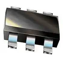
MOSFET, P-CH, 20V, 1.3A, SC-70
- Manufacturer: VISHAY
- Product type: Dual MOSFETs
- Channel Type:P Channel; Drain Source Voltage Vds N Channel:-; Drain Source Voltage Vds P Channel:20V; Continuous Drain Current Id N Channel:-; Continuous Drain Current Id P Channel:1.3A 36
- No. of Pins: 6Pins
- Qualification: -
| Delivery and price | |
|---|---|
| Units per pack | 3000 |
| Price | 0.173 € |
| Current stock | 1000+ |
| Lead time | 30 days |
**Si1967DH**

**==> picture [59 x 48] intentionally omitted <==**

Vishay Siliconix

## **Dual P-Channel 20 V (D-S) MOSFET**

**==> picture [44 x 91] intentionally omitted <==**

|**PRODUCT SUMMARY**|**PRODUCT SUMMARY**|**PRODUCT SUMMARY**|**PRODUCT SUMMARY**|**FEATURES**<br>•<br>**Halogen-free According to IEC 61249-2-21**<br>**Definition**<br>•<br>TrenchFET®Power MOSFET<br>•<br>PWM Optimized<br>•<br>Compliant to RoHS Directive 2002/95/EC|
|---|---|---|---|---|
|**VDS (V)**|**RDS(on) (**Ω**)**|**ID (A)**|**Qg (Typ.)**||
|- 20|0.490 at VGS= - 4.5 V<br>|- 1.3a|1.6 nC||
||0.640 at VGS= - 2.5 V|- 1.2|||
||0.790 at VGS= - 1.8 V|- 1.0|||


## **APPLICATIONS**

**==> picture [493 x 144] intentionally omitted <==**

**----- Start of picture text -----**<br>
SOT-363<br>SC-70 (6-LEADS)  • Load Switch for Portable Devices<br>S1 S2<br>S1 1 6 D1<br>Marking Code<br>G1 2 5 G2 DF XX<br>Lot Traceability G1 G2<br>and Date Code<br>D2 3 4 S2 Part # Code<br>Top View<br>Ordering Information:  Si1967DH-T1-E3 (Lead (Pb)-free) D1 D2<br>Si1967DH-T1-GE3 (Lead (Pb)-free and Halogen-free) P-Channel MOSFET P-Channel MOSFET<br>YY<br>**----- End of picture text -----**<br>


**Ordering Information:** Si1967DH-T1-E3 (Lead (Pb)-free) Si1967DH-T1-GE3 (Lead (Pb)-free and Halogen-free)

|**ABSOLUTE MAXIMUM RATINGS**TA= 25 °C, unless otherwise noted|**ABSOLUTE MAXIMUM RATINGS**TA= 25 °C, unless otherwise noted|**ABSOLUTE MAXIMUM RATINGS**TA= 25 °C, unless otherwise noted|**ABSOLUTE MAXIMUM RATINGS**TA= 25 °C, unless otherwise noted||
|---|---|---|---|---|
|**Parameter**||**Symbol**|**Limit**|**Unit**|
|Drain-Source Voltage||VDS|- 20|V|
|Gate-Source Voltage||VGS|± 8||
|Continuous Drain Current (TJ= 150 °C)|TC= 25 °C|ID|- 1.3a|A|
||TC= 70 °C||- 1.1||
||TA= 25 °C||- 1.0b, c||
||TA= 70 °C||- 0.83b, c||
|Pulsed Drain Current||IDM|- 3||
|Continuous Source-Drain Diode Current|TC= 25 °C|IS|- 1||
||TA= 25 °C||- 0.6b, c||
|Maximum Power Dissipation|TC= 25 °C|PD|1.25|W|
||TC= 70 °C||0.8||
||TA= 25 °C||0.74b, c||
||TA= 70 °C||0.47b, c||
|Operating Junction and Storage Temperature|Range|TJ, Tstg|- 55 to 150|°C|


|**THERMAL RESISTANCE RATINGS**|**THERMAL RESISTANCE RATINGS**|**THERMAL RESISTANCE RATINGS**|**THERMAL RESISTANCE RATINGS**|**THERMAL RESISTANCE RATINGS**|**THERMAL RESISTANCE RATINGS**|
|---|---|---|---|---|---|
|**Parameter**||**Symbol**|**Typical**|**Maximum**|**Unit**|
|Maximum Junction-to-Ambientb, d|t≤5 s|RthJA|130|170|°C/W|
|Maximum Junction-to-Foot (Drain)|Steady State|RthJF|80|100||


Notes:

a. Package limited.

b. Surface mounted on 1" x 1" FR4 board.

c. t = 5 s.

- d. Maximum under steady state conditions is 220 °C/W.

Document Number: 68784 S10-0721-Rev. B, 29-Mar-10

www.vishay.com 1

**Si1967DH**

## Vishay Siliconix

**==> picture [59 x 48] intentionally omitted <==**

|**SPECIFICATIONS**TJ= 25 °C, unless otherwise noted|**SPECIFICATIONS**TJ= 25 °C, unless otherwise noted|**SPECIFICATIONS**TJ= 25 °C, unless otherwise noted|||||
|---|---|---|---|---|---|---|
|**Parameter**|**Symbol**|**Test Conditions**|**Min.**|**Typ.**|**Max.**|**Unit**|
|**Static**|||||||
|Drain-Source Breakdown Voltage|VDS|VGS= 0 V, ID= - 250 µA|- 20|||V|
|VDSTemperature Coefficient|ΔVDS/TJ|ID= - 250 µA||- 20||mV/°C|
|VGS(th)Temperature Coefficient|ΔVGS(th)/TJ|||2|||
|Gate-Source Threshold Voltage|VGS(th)|VDS= VGS, ID= - 250 µA|- 0.4||- 1.0|V|
|Gate-Source Leakage|IGSS|VDS= 0 V, VGS= ± 8 V|||± 100|nA|
|Zero Gate Voltage Drain Current|IDSS|VDS= - 20 V, VGS= 0 V|||- 1|µA|
|||VDS= - 20 V, VGS= 0 V, TJ= 85 °C|||- 10||
|On-State Drain Currenta|ID(on)|VDS≤- 5 V, VGS= - 4.5 V|- 3|||A|
|Drain-Source On-State Resistancea|RDS(on)|VGS=- 4.5 V, ID= - 0.91 A||0.390|0.490|Ω|
|||VGS=- 2.5 V, ID= - 0.8 A||0.500|0.640||
|||VGS=- 1.8 V, ID= - 0.25 A||0.640|0.790||
|Forward Transconductancea|gfs|VDS= - 10 V, ID= - 0.91 A||2||S|
|**Dynamicb**|||||||
|Input Capacitance|Ciss|VDS= - 10 V, VGS= 0 V, f = 1 MHz||110||pF|
|Output Capacitance|Coss|||26|||
|Reverse Transfer Capacitance|Crss|||16|||
|Total Gate Charge|Qg|VDS= - 10 V, VGS= - 8 V, ID= - 1.1 A||2.6|4.0|nC|
|||VDS= - 10 V, VGS= - 4.5 V, ID= - 1.1 A||1.6|2.4||
|Gate-Source Charge|Qgs|||0.36|||
|Gate-Drain Charge|Qgd|||0.33|||
|Gate Resistance|Rg|f = 1 MHz||7.5||Ω|
|Turn-On Delay Time|td(on)|VDD= - 10 V, RL= 12Ω<br>ID ≅- 0.83 A, VGEN= - 4.5 V, Rg= 1Ω||12|20|ns|
|Rise Time|tr|||27|40||
|Turn-Off Delay Time|td(off)|||15|25||
|Fall Time|tf|||10|15||
|Turn-On Delay Time|td(on)|VDD= - 10 V, RL= 12Ω<br>ID ≅- 0.83 A, VGEN= - 8 V, Rg= 1Ω||2|5||
|Rise Time|tr|||12|20||
|Turn-Off Delay Time|td(off)|||12|20||
|Fall Time|tf|||10|15||
|**Drain-Source Body Diode Characteristics**|||||||
|Continuous Source-Drain Diode Current|IS|TC= 25 °C|||- 1.0|A|
|Pulse Diode Forward Currenta|ISM||||- 3.0||
|Body Diode Voltage|VSD|IS= - 0.9 A||- 0.8|- 1.2|V|
|Body Diode Reverse Recovery Time|trr|IF= - 0.83 A, dI/dt = 100 A/µs, TJ= 25 °C||25|50|ns|
|Body Diode Reverse Recovery Charge|Qrr|||15|30|nC|
|Reverse Recovery Fall Time|ta|||12||ns|
|Reverse Recovery Rise Time|tb|||13|||


Notes:

a. Pulse test; pulse width ≤ 300 µs, duty cycle ≤ 2 %

b. Guaranteed by design, not subject to production testing.

_Stresses beyond those listed under “Absolute Maximum Ratings” may cause permanent damage to the device. These are stress ratings only, and functional operation of the device at these or any other conditions beyond those indicated in the operational sections of the specifications is not implied. Exposure to absolute maximum rating conditions for extended periods may affect device reliability._

www.vishay.com 2

Document Number: 68784 S10-0721-Rev. B, 29-Mar-10

**Si1967DH**

Vishay Siliconix

**==> picture [59 x 48] intentionally omitted <==**

## **TYPICAL CHARACTERISTICS** 25 °C, unless otherwise noted

**==> picture [224 x 619] intentionally omitted <==**

**----- Start of picture text -----**<br>
3.0<br>VGS = 5 V thru 2.5 V<br>2.5<br>2.0 VGS = 2 V<br>1.5<br>1.0<br>VGS = 1.5 V<br>0.5<br>VGS = 1 V<br>0.0<br>0.0 0.5 1.0 1.5 2.0 2.5 3.0<br>VDS - Drain-to-Source Voltage (V)<br>Output Characteristics<br>1.2<br>1.0<br>0.8 VGS = 1.8 V<br>0.6 VGS = 2.5 V<br>0.4<br>VGS = 4.5 V<br>0.2<br>0.0<br>0.0 0.5 1.0 1.5 2.0 2.5 3.0<br>ID - Drain Current (A)<br>On-Resistance vs. Drain Current and Gate Voltage<br>8<br>ID = 1 A<br>6<br>VDS = 10 V<br>4<br>VDS = 16 V<br>2<br>0<br>0.0 0.5 1.0 1.5 2.0 2.5 3.0<br>Qg - Total Gate Charge (nC)<br>Gate Charge<br>- Drain Current (A)<br>I D<br>)Ω<br>- On-Resistance (<br>DS(on)<br>R<br>- Gate-to-Source Voltage (V)<br>GS<br>V<br>**----- End of picture text -----**<br>


**==> picture [192 x 9] intentionally omitted <==**

**----- Start of picture text -----**<br>
On-Resistance vs. Drain Current and Gate Voltage<br>**----- End of picture text -----**<br>


**==> picture [217 x 187] intentionally omitted <==**

**----- Start of picture text -----**<br>
1.0<br>0.8<br>0.6<br>0.4<br>TC = 25 °C<br>TC = 125 °C<br>0.2<br>TC = - 55 °C<br>0.0<br>0.0 0.4 0.8 1.2 1.6 2.0<br>VGS - Gate-to-Source Voltage (V)<br>- Drain Current (A)<br>I D<br>**----- End of picture text -----**<br>


**==> picture [93 x 7] intentionally omitted <==**

**----- Start of picture text -----**<br>
Transfer Characteristics<br>**----- End of picture text -----**<br>


**==> picture [223 x 408] intentionally omitted <==**

**----- Start of picture text -----**<br>
200<br>160<br>120 Ciss<br>80<br>Coss<br>40<br>Crss<br>0<br>0 3 6 9 12<br>VDS - Drain-to-Source Voltage (V)<br>Capacitance<br>1.4<br>VGS = 4.5 V, 2.5 V; ID = 0.91 A<br>1.3<br>1.2<br>1.1<br>VGS = 1.8 V; ID = 0.12 A<br>1.0<br>0.9<br>0.8<br>0.7<br>- 50 - 25 0 25 50 75 100 125 150<br>TJ - Junction Temperature (°C)<br>On-Resistance vs. Junction Temperature<br>C - Capacitance (pF)<br>- On-Resistance<br>(Normalized)<br>DS(on)<br>R<br>**----- End of picture text -----**<br>


Document Number: 68784 S10-0721-Rev. B, 29-Mar-10

www.vishay.com

3

**Si1967DH**

## Vishay Siliconix

**==> picture [59 x 48] intentionally omitted <==**

## **TYPICAL CHARACTERISTICS** 25 °C, unless otherwise noted

**==> picture [222 x 184] intentionally omitted <==**

**----- Start of picture text -----**<br>
10<br>TJ = 150 °C TJ = 25 °C<br>1<br>0.1<br>0.0 0.2 0.4 0.6 0.8 1.0 1.2 1.4<br>VSD - Source-to-Drain Voltage (V)<br>- Source Current (A)<br>I S<br>**----- End of picture text -----**<br>


**Source-Drain Diode Forward Voltage**

**==> picture [215 x 187] intentionally omitted <==**

**----- Start of picture text -----**<br>
2.0<br>ID = - 0.91 A<br>1.6<br>1.2<br>0.8 TJ = 125 °C<br>0.4<br>TJ = 25 °C<br>0.0<br>0 1 2 3 4 5<br>VGS - Gate-to-Source Voltage (V)<br>)Ω<br>- On-Resistance (<br>DS(on)<br>R<br>**----- End of picture text -----**<br>


**==> picture [162 x 8] intentionally omitted <==**

**----- Start of picture text -----**<br>
On-Resistance vs. Gate-to-Source Voltage<br>**----- End of picture text -----**<br>


**==> picture [489 x 195] intentionally omitted <==**

**----- Start of picture text -----**<br>
0.80 5<br>0.75<br>4<br>0.70<br>0.65 3<br>ID = 250 µA<br>0.60<br>2<br>0.55<br>0.50<br>1<br>0.45<br>0.40 0<br>- 50 - 25 0 25 50 75 100 125 150 0.01  0.1  1 10  100  600<br>TJ - Temperature (°C) Time (s)<br>Threshold Voltage Single Pulse Power<br>(V) )W<br>(  r<br>e<br>w<br>VGS(th) Po<br>**----- End of picture text -----**<br>


**==> picture [214 x 200] intentionally omitted <==**

**----- Start of picture text -----**<br>
10<br>Limited by RDS(on)*<br>1<br>1 ms<br>10 ms<br>0.1<br>TA = 25 °C 100 ms<br>Single Pulse 1 s, 10 s<br>DC<br>BVDSS Limited<br>0.01<br>0.1 1 10 100<br>VDS - Drain-to-Source Voltage (V)<br>* VGS > minimum VGS at which RDS(on) is specified<br>Safe Operating Area, Junction-to-Ambient<br>Drain Current (A)<br>-<br>ID<br>**----- End of picture text -----**<br>


www.vishay.com 4

Document Number: 68784 S10-0721-Rev. B, 29-Mar-10

**Si1967DH**

Vishay Siliconix

**==> picture [59 x 48] intentionally omitted <==**

## **TYPICAL CHARACTERISTICS** 25 °C, unless otherwise noted

**==> picture [485 x 198] intentionally omitted <==**

**----- Start of picture text -----**<br>
1.6 1.4<br>1.2<br>1.2<br>1.0<br>Package Limited<br>0.8<br>0.8<br>0.6<br>0.4<br>0.4<br>0.2<br>0.0 0.0<br>0 25 50 75 100 125 150 25 50 75 100 125 150<br>TC - Case Temperature (°C) T C  - Case Temperature (°C)<br>Current Derating* Power, Junction-to-Foot<br>Drain Current (A)<br>ID- wer Dissipation (W) Po<br>**----- End of picture text -----**<br>


* The power dissipation PD is based on TJ(max) = 150 °C, using junction-to-case thermal resistance, and is more useful in settling the upper dissipation limit for cases where additional heatsinking is used. It is used to determine the current rating, when this rating falls below the package limit.

Document Number: 68784 S10-0721-Rev. B, 29-Mar-10

www.vishay.com

5

**Si1967DH**

## Vishay Siliconix

**==> picture [59 x 48] intentionally omitted <==**

## **TYPICAL CHARACTERISTICS** 25 °C, unless otherwise noted

**==> picture [470 x 182] intentionally omitted <==**

**----- Start of picture text -----**<br>
2<br>1<br>Duty Cycle = 0.5<br>0.2<br>Notes:<br>0.1<br>0.1 P DM<br>0.05<br>t 1<br>0.02 1. Duty Cycle, D = t 2  t t 1 2<br>2. Per Unit Base = R thJA  = 220 °C/W<br>3. T JM - TA = PDMZthJA [(t)]<br>Single Pulse 4. Surface Mounted<br>0.01<br>10 [-4] 10 [-3] 10 [-2] 10 [-1] 1 10 100 600<br>Square Wave Pulse Duration (s)<br>t n<br>i T i t r e s n a ev  d e n a e p c<br>c e  I m<br>f f E de    la r m e<br>z  h<br>i l a  T<br>m r o<br>N<br>**----- End of picture text -----**<br>


**Normalized Thermal Transient Impedance, Junction-to-Ambient**

**==> picture [470 x 182] intentionally omitted <==**

**----- Start of picture text -----**<br>
2<br>1<br>Duty Cycle = 0.5<br>0.2<br>0.1<br>0.1  0.05<br>0.02<br>Single Pulse<br>0.01<br>10 [-4] 10 [-3] 10 [-2] 10 [-1] 1 10<br>Square Wave Pulse Duration (s)<br>t n<br>i T i t e s n a r ev  d e c n a e p<br>c e  I m<br>f f E de    la m r e<br>z  h<br>i l a  T<br>m r o<br>N<br>**----- End of picture text -----**<br>


**Normalized Thermal Transient Impedance, Junction-to-Foot**

_Vishay Siliconix maintains worldwide manufacturing capability. Products may be manufactured at one of several qualified locations. Reliability data for Silicon Technology and Package Reliability represent a composite of all qualified locations. For related documents such as package/tape drawings, part marking, and reliability data, see www.vishay.com/ppg?68784._

www.vishay.com 6

Document Number: 68784 S10-0721-Rev. B, 29-Mar-10

## ~~a~~ **Package Information Vishay Siliconix**

**==> picture [482 x 192] intentionally omitted <==**

**----- Start of picture text -----**<br>
6 5 4 E1 E oteeee DimAA1 ee Min 0.90– Nom –– Max 1.100.10 0.035 Min – Nom –– ee Max 0.0430.004<br>1 2 3 a A2 0.80 – 1.00 0.031 – 0.039<br>-B- ee b 0.15 – 0.30 0.006 – 0.012<br>ee c 0.10 – 0.25 0.004 – 0.010<br>e b<br>e1 ee D 1.80 2.00 2.20 0.071 0.079 0.087<br>a ee E 1.80 2.10 2.40 0.071 0.083 0.094<br>D -A-<br>- c ee E1 1.15 1.25 1.35 0.045 0.049 0.053<br>a e 0.65BSC 0.026BSC<br>A2 A ee e1 1.20 1.30 1.40 0.047 0.051 0.055<br>ee L 0.10 0.20 0.30 0.004 0.008 0.012<br>We | L ee 7 Nom 7 Nom<br>A1 ECN: S-03946—Rev. B, 09-Jul-01<br>DWG:  5550<br>**----- End of picture text -----**<br>


Document Number: 71154 06-Jul-01

www.vishay.com

**1**

**AN816**

# **Vishay Siliconix**

## **Dual-Channel LITTLE FOOT** ® **6-Pin SC-70 MOSFET Copper Leadframe Version Recommended Pad Pattern and Thermal Performance**

## INTRODUCTION

The new dual 6-pin SC-70 package with a copper leadframe enables improved on-resistance values and enhanced thermal  performance as compared to the existing 3-pin and 6-pin packages with Alloy 42 leadframes. These devices are intended for small  to medium load applications where a miniaturized package is required. Devices in this package come in a range  of on-resistance values, in n-channel and p-channel versions. This technical note discusses pin-outs, package outlines, pad patterns, evaluation board layout, and thermal performance for the dual-channel version.

## PIN-OUT

Figure 1 shows the pin-out description and Pin 1 identification for the dual-channel SC-70 device in the 6-pin configuration. Both n-and p-channel devices are available in this package – the drawing example below illustrates the p-channel device.

**==> picture [113 x 132] intentionally omitted <==**

**----- Start of picture text -----**<br>
SOT-363<br>SC-70 (6-LEADS)<br>S1 1 6 D1<br>G1 2 5 G2<br>D2 3 4 S2<br>t e<br>Top View<br>FIGURE  1.<br>**----- End of picture text -----**<br>


**==> picture [216 x 239] intentionally omitted <==**

**----- Start of picture text -----**<br>
87 (mil)<br>26 (mil)<br>6 5 4<br>96 (mil)<br>71 (mil)<br>aay<br>48 (mil)<br>23 (mil) 61 (mil)<br>1 2 3<br>0.0 (mil)<br>“gon<br>8 (mil)<br>26 (mil)<br>16 (mil)<br>FIGURE  2. SC-70 (6 leads) Dual<br>**----- End of picture text -----**<br>


## EVALUATION BOARD FOR THE DUALCHANNEL SC70-6

The 6-pin SC-70 evaluation board (EVB) shown in Figure 3 measures 0.6 in. by 0.5 in. The copper pad traces are the same as described in the previous section, _Basic Pad Patterns_ . The board allows for examination from the outer pins to the 6-pin DIP connections, permitting test sockets to be used in evaluation testing.

For package dimensions see outline drawing SC-70 (6-Leads) (http://www.vishay.com/doc?71154)

The thermal performance of the dual 6-pin SC-70 has been measured on the EVB, comparing both the copper and Alloy 42 leadframes. This test was then repeated using the 1-inch[2] PCB with dual-side copper coating.

## BASIC PAD PATTERNS

See Application Note 826, _Recommended Minimum Pad Patterns With Outline Drawing Access for Vishay Siliconix MOSFET_ s, (http://www.vishay.com/doc?72286) for the SC-70 6-pin basic pad layout and dimensions. This pad pattern is sufficient for the low-power applications for which this package is intended. Increasing the drain pad pattern (Figure 2) yields a reduction in thermal resistance and is a preferred footprint.

A helpful way of displaying the thermal performance of the 6-pin SC-70 dual copper leadframe is to compare it to the traditional Alloy 42 version.

Document Number:  71405 12-Dec-03

www.vishay.com

**1**

**AN816** ~~CCNISSHA~~ Y **Vishay Siliconix**

**==> picture [117 x 132] intentionally omitted <==**

**----- Start of picture text -----**<br>
Front of Board SC70-6<br>S1 D1<br>G1 G2<br>a \ Le.<br>ei He<br>D2 S2<br>eo e<br>SC70 − 6 DUAL<br>**----- End of picture text -----**<br>


**==> picture [84 x 7] intentionally omitted <==**

**----- Start of picture text -----**<br>
Back of Board SC70-6<br>**----- End of picture text -----**<br>


**==> picture [110 x 18] intentionally omitted <==**

**----- Start of picture text -----**<br>
vishay.com<br>**----- End of picture text -----**<br>


**FIGURE  3.**

## THERMAL PERFORMANCE

## **Junction-to-Foot Thermal Resistance (the Package Performance)**

Thermal performance for the dual SC-70 6-pin package is measured as junction-to-foot thermal resistance, in which the “foot” is the drain lead of the device as it connects with the body. The junction-to-foot thermal resistance for this device is typically 80 . C/W, with a maximum thermal resistance of approximately 100 C/W. This data compares favorably with another compact, dual-channel package – the dual TSOP-6 – which features a typical thermal resistance of 75 C/W and a maximum of 90 C/W.

**==> picture [241 x 104] intentionally omitted <==**

**----- Start of picture text -----**<br>
CP COOPER LEADFRAME<br>Room Ambient 25 C Elevated Ambient 60 C<br>ee ee<br>PD - —,— TJ(max)R JA TA PD oo TJ(max)R JA TA<br>PD - 150224 [o] C [o] 7 C 25W [o] C PD ae 150224 [o] C [o] C 60W [o] C<br>PD 558 mW PD 402 mW<br>**----- End of picture text -----**<br>


Although they are intended for low-power applications, devices in the 6-pin SC-70 dual-channel configuration will handle power dissipation in excess of 0.5 W.

## TESTING

## **Power Dissipation**

The typical R θ JA for the dual-channel 6-pin SC-70 with a copper leadframe is 224 C/W steady-state, compared to 413 C/W for the Alloy 42 version. All figures are based on the 1-inch[2] FR4 test board. The following example shows how the thermal resistance impacts power dissipation for the dual 6-pin SC-70 package at varying ambient temperatures.

## _**Alloy 42 Leadframe**_

|ALLOY 42 LEADFRAME<br>~~CP~~<br>~~ee~~|ALLOY 42 LEADFRAME<br>~~CP~~<br>~~ee~~|
|---|---|
|**Room Ambient 25 C**<br>~~ee~~|**Elevated Ambient 60 C**|
|PD<br>TJ(max)<br>TA<br>R JA<br>PD<br>150oC<br>25oC<br>413oC W<br>PD<br>303 mW<br>~~ee~~<br>= ~~——~~<br>—|PD<br>TJ(max)<br>TA<br>R JA<br>PD<br>150oC<br>60oC<br>413oC W<br>PD<br>218 mW<br>_ ~~——~~<br>-|


To further aid the comparison of copper and Alloy 42 leadframes, Figures 4 and 5 illustrate the dual-channel 6-pin SC-70 thermal performance on two different board sizes and pad patterns. The measured steady-state values of R θ JA for the dual 6-pin SC-70 with varying leadframes are as follows:

|LITTLE FOOT 6-PIN SC-70<br>~~Cd~~<br>~~es~~|LITTLE FOOT 6-PIN SC-70<br>~~Cd~~<br>~~es~~|LITTLE FOOT 6-PIN SC-70<br>~~Cd~~<br>~~es~~|
|---|---|---|
|~~ee~~|**Alloy 42**<br>~~ee~~<br>~~es~~<br>~~ee~~|**Copper**<br>~~ee~~<br>~~ee~~|
|1) Minimum recommended pad pattern on<br>the EVB board (see Figure 3).<br>~~ee~~|518 C/W<br>~~es~~<br>~~ee~~<br>~~ee~~<br>~~ee~~|344 C/W<br>~~ee~~<br>~~ee~~<br>~~ee~~|
|2) Industry standard 1-inch2PCB with<br>maximum copper both sides.<br>~~ee~~|413 C/W<br>~~ee ~~<br>~~ee~~<br>~~ee~~|224 C/W<br> ~~ee~~<br>~~ee~~<br>~~ee~~|


The results indicate that designers can reduce thermal resistance ( θ JA) by 34% simply by using the copper leadframe device as opposed to the Alloy 42 version. In this example, a 174 C/W reduction was achieved without an increase in board area. If an increase in board size is feasible, a further 120 C/W ° reduction can be obtained by utilizing a 1-inch[2] . PCB area.

The Dual copper leadframe versions have the following suffix:

|Dual:<br>Compl.:|Si19xxEDH<br>Si15xxEDH|
|---|---|


Document Number:  71405 12-Dec-03

www.vishay.com

**2**

**AN816**

**==> picture [486 x 272] intentionally omitted <==**

**----- Start of picture text -----**<br>
Vishay Siliconix<br>Vv<br>500 500<br>400 400<br>a =n<br>300 300<br>Alloy<br>H Alloy 42 e  a  42<br>200 200<br>eae Copper Mo<br>100 100<br>WA 2A fl Copper<br>0 A 0<br>10 [-5] 10 [-4] 10 [-3] 10 [-2] 10 [-1] 1 10 100 1000 10 [-5] 10 [-4] 10 [-3] 10 [-2] 10 [-1] 1 10 100 1000<br>Time (Secs) Time (Secs)<br>FIGURE  4. Dual SC70-6 Thermal Performance on EVB FIGURE  5. Dual SC70-6 Comparison on 1-inch [2]  PCB<br>Thermal Resistance (C/W) Thermal Resistance (C/W)<br>**----- End of picture text -----**<br>


## **Vishay Siliconix**

Document Number:  71405 12-Dec-03

www.vishay.com

**3**

**Application Note 826**

Vishay Siliconix

**==> picture [59 x 50] intentionally omitted <==**

## **RECOMMENDED MINIMUM PADS FOR SC-70: 6-Lead**

**==> picture [178 x 217] intentionally omitted <==**

**----- Start of picture text -----**<br>
0.067<br>(1.702)<br>0.016 0.026 0.010<br>(0.406) (0.648) (0.241)<br>0.026 (0.648)<br>0.096 (2.438) 0.045 (1.143)<br>**----- End of picture text -----**<br>


**==> picture [95 x 16] intentionally omitted <==**

**----- Start of picture text -----**<br>
Recommended Minimum Pads<br>Dimensions in Inches/(mm)<br>**----- End of picture text -----**<br>


**==> picture [48 x 6] intentionally omitted <==**

**----- Start of picture text -----**<br>
Return to Index<br>**----- End of picture text -----**<br>


Return to Index

##

www.vishay.com 18

Document Number: 72602 Revision: 21-Jan-08

**Legal Disclaimer Notice** Vishay

www.vishay.com

**==> picture [59 x 48] intentionally omitted <==**

## **Disclaimer**

ALL PRODUCT, PRODUCT SPECIFICATIONS AND DATA ARE SUBJECT TO CHANGE WITHOUT NOTICE TO IMPROVE RELIABILITY, FUNCTION OR DESIGN OR OTHERWISE.

Vishay Intertechnology, Inc., its affiliates, agents, and employees, and all persons acting on its or their behalf (collectively, “Vishay”), disclaim any and all liability for any errors, inaccuracies or incompleteness contained in any datasheet or in any other disclosure relating to any product.

Vishay makes no warranty, representation or guarantee regarding the suitability of the products for any particular purpose or the continuing production of any product.  To the maximum extent permitted by applicable law, Vishay disclaims (i) any and all liability arising out of the application or use of any product, (ii) any and all liability, including without limitation special, consequential or incidental damages, and (iii) any and all implied warranties, including warranties of fitness for particular purpose, non-infringement and merchantability.

Statements regarding the suitability of products for certain types of applications are based on Vishay’s knowledge of typical requirements that are often placed on Vishay products in generic applications.  Such statements are not binding statements about the suitability of products for a particular application.  It is the customer’s responsibility to validate that a particular product with the properties described in the product specification is suitable for use in a particular application. Parameters provided in datasheets and / or specifications may vary in different applications and performance may vary over time.  All operating parameters, including typical parameters, must be validated for each customer application by the customer’s technical experts.  Product specifications do not expand or otherwise modify Vishay’s terms and conditions of purchase, including but not limited to the warranty expressed therein.

Except as expressly indicated in writing, Vishay products are not designed for use in medical, life-saving, or life-sustaining applications or for any other application in which the failure of the Vishay product could result in personal injury or death. Customers using or selling Vishay products not expressly indicated for use in such applications do so at their own risk. Please contact authorized Vishay personnel to obtain written terms and conditions regarding products designed for such applications.

No license, express or implied, by estoppel or otherwise, to any intellectual property rights is granted by this document or by any conduct of Vishay.  Product names and markings noted herein may be trademarks of their respective owners.

_**© 2017 VISHAY INTERTECHNOLOGY, INC. ALL RIGHTS RESERVED**_

Revision: 08-Feb-17

Document Number: 91000

**1**
Updated at June 9, 2026
Vishay is a global leader in the manufacturing of discrete semiconductors and passive electronic components. Renowned for its exceptional quality and engineering expertise, the company produces highly reliable solutions that drive innovation across the industrial, automotive, telecommunications, and consumer electronics markets. From advanced factory automation to vehicle electrification, Vishay components provide the foundational building blocks for modern electronic design. The company's expansive portfolio is heavily focused on efficient power management, signal routing, and energy storage. Within its passive component lineup, Vishay is recognized for its extensive array of high-performance capacitors, including robust aluminium electrolytic, film, and polymer variants, alongside highly efficient power inductors. In the realm of discrete semiconductors, Vishay is a premier manufacturer of single and dual MOSFETs, as well as a vast selection of Schottky, Zener, and fast-recovery rectifier diodes designed for demanding power applications. Furthermore, Vishay delivers industry-leading circuit protection and thermal management solutions. With a broad offering of transient voltage suppressors (TVS diodes) and temperature-sensing NTC thermistors, these components are engineered to safeguard sensitive circuitry against both electrical and thermal overstress. By combining this vital mix of advanced discretes and passives, Vishay enables engineers to develop robust, space-saving, and highly resilient electronic systems.
About Novapart
Novapart is a B2B electronic component broker specialising in stock shortages and cost reduction. We source hard-to-find parts and identify compliant alternatives across a catalogue of 410,000+ components from 500+ manufacturers.
Learn more →Stock Shortage Specialist
When a component is unavailable, discontinued or has an unacceptable lead time, we tap into our network of vetted European and Asian distributors to source what you need — without compromising on quality or traceability.
Request a quote →Compliant Alternatives
We identify pin-to-pin, electrically equivalent substitutes that meet the same certifications (RoHS, AEC-Q100, REACH) as your original specification — validated against datasheets, not just part numbers. Often at a lower cost.
BOM Analysis service →