
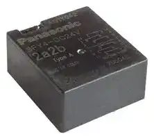


SFY2-DC12V
Safety Relay, 12 VDC, DPST-NO, DPST-NC, SFY Series, Through Hole, 6 A, Solder
- Manufacturer: PANASONIC
- Product type: Safety Relays
- Coil Voltage:12VDC; Contact Configuration:DPST-NO, DPST-NC; Product Range:SF Series; Relay Mounting:Through Hole; Contact Current:6A; Relay Terminals:Solder; Contact Voltage AC N
- SVHC: No SVHC (23-Jan-2024)
- IP Rating: -
- Coil Voltage: 12VDC
- Product Range: SFY Series
- Relay Mounting: Through Hole
- Contact Current: 6A
- Relay Terminals: Solder
- Contact Material: Silver Nickel Alloy
- Approvals & Standards: UL
- Contact Configuration: DPST-NO, DPST-NC
- Contact Voltage AC Nom: 250V
- Contact Voltage DC Nom: 30V
| Delivery and price | |
|---|---|
| Units per pack | 50 |
| Price | 19.66 € |
| Current stock | 25+ |
| Lead time | 30 days |
4-pole (2 Form A 2 Form B, 3 Form A 1 Form B)

## **Compact Relay Family with Forcibly Guided Contacts**

## **FEATURES**

## **1. Forcibly guided contact structure Relay complies with EN 50205, Type A**

Equipped with forcibly guided contact structure that enables detection of contact welding and construction of safety circuit.

## **2. Small size**

## **3. Different contact configurations:**

|Type|L×W×H(mminch)|
|---|---|
|2 Form A 2 Form B,<br>3 Form A 1 Form B|31.0×28.6×14.5<br>1.220×1.126×.571|
|4 Form A 2 Form B,<br>5 Form A 1 Form B|39.0×28.6×14.5<br>1.535×1.126×.571|


## SF-Y RELAYS

## **TYPICAL APPLICATIONS**

**1. Emergency stop switches**

**2. Machine safety engineering**

**3. Safety control units**

**4. Automation technology**

**5. Elevators**

**6. Escalators**

**7. Overcurrent protection with monitor contact**

## **4. Low profile: 14.5 mm .571 inch**

## **5. Insulation according to EN 60664-1:**

Overvoltage category III, Pollution degree 2, 250V AC

6-pole (4 Form A 2 Form B, 5 Form A 1 Form B)

## **RoHS compliant**

**• Reinforced insulation:** Clearance and creepage 5.5 mm .217 inch

(between all contacts and between contact NO4 and coil)

**• Basic insulation:**

Clearance 3 mm .118 inch and creepage 4 mm .157 inch (between all contacts and between contact NC3 and coil)

## **ORDERING INFORMATION**

## **SFY**

Contact arrangement

2: 2 Form A 2 Form B

3: 3 Form A 1 Form B

4: 4 Form A 2 Form B

5: 5 Form A 1 Form B

Nominal coil voltage DC 5, 12, 16, 18, 21, 24V

Notes: Please consult us about other coil voltages. Gold-clad contact type available on request.

ASCTB317E   201512-T

–1–

SFY

## **TYPES**

|**TYPES**|**TYPES**|||
|---|---|---|---|
|Contact arrangement||Nominal coil voltage|Part No.|
|4-pole|2 Form A 2 Form B<br>3 Form A 1 Form B|5 V DC|SFY2-DC5V|
|||12 V DC|SFY2-DC12V|
|||16 V DC|SFY2-DC16V|
|||18 V DC|SFY2-DC18V|
|||21 V DC|SFY2-DC21V|
|||24 V DC|SFY2-DC24V|
|||5 V DC|SFY3-DC5V|
|||12 V DC|SFY3-DC12V|
|||16 V DC|SFY3-DC16V|
|||18 V DC|SFY3-DC18V|
|||21 V DC|SFY3-DC21V|
|||24 V DC|SFY3-DC24V|
|6-pole|4 Form A 2 Form B<br>5 Form A 1 Form B|5 V DC|SFY4-DC5V|
|||12 V DC|SFY4-DC12V|
|||16 V DC|SFY4-DC16V|
|||18 V DC|SFY4-DC18V|
|||21 V DC|SFY4-DC21V|
|||24 V DC|SFY4-DC24V|
|||5 V DC|SFY5-DC5V|
|||12 V DC|SFY5-DC12V|
|||16 V DC|SFY5-DC16V|
|||18 V DC|SFY5-DC18V|
|||21 V DC|SFY5-DC21V|
|||24 V DC|SFY5-DC24V|
|Standard packing: Tube 20 pcs.||||


## **RATING**

## **1. Coil data**

|**RATING**<br>**1. Coil data**|**RATING**<br>**1. Coil data**||||||||
|---|---|---|---|---|---|---|---|---|
|Contact arrangement||Nominal coil<br>voltage|Pick-up voltage<br>(at 20°C68°F)|Drop-out voltage<br>(at 20°C68°F)|Nominal<br>operating current<br>[±10%]<br>(at 20°C68°F)|Coil resistance<br>[±10%]<br>(at 20°C68°F)|Nominal<br>operating power<br>(at 20°C68°F)|Max. applied<br>voltage<br>(at 20°C68°F)|
|4-pole|2 Form A 2 Form B|5V DC|75%V or less of<br>nominal voltage<br>(Initial)|15%V or more of<br>nominal voltage<br>(Initial)|134mA|38Ω|670mW|120%V of<br>nominal voltage|
|||12V DC|||56mA|215Ω|||
|||16V DC|||42mA|380Ω|||
|||18V DC|||37mA|483Ω|||
|||21V DC|||32mA|666Ω|||
|||24V DC|||28mA|864Ω|||
||3 Form A 1 Form B|5V DC|||134mA|38Ω|||
|||12V DC|||56mA|215Ω|||
|||16V DC|||42mA|380Ω|||
|||18V DC|||37mA|483Ω|||
|||21V DC|||32mA|666Ω|||
|||24V DC|||28mA|864Ω|||
|6-pole|4 Form A 2 Form B|5V DC|||134mA|38Ω|||
|||12V DC|||56mA|215Ω|||
|||16V DC|||42mA|380Ω|||
|||18V DC|||37mA|483Ω|||
|||21V DC|||32mA|666Ω|||
|||24V DC|||28mA|864Ω|||
||5 Form A 1 Form B|5V DC|||134mA|38Ω|||
|||12V DC|||56mA|215Ω|||
|||16V DC|||42mA|380Ω|||
|||18V DC|||37mA|483Ω|||
|||21V DC|||32mA|666Ω|||
|||24V DC|||28mA|864Ω|||


ASCTB317E   201512-T

–2–

SFY

## **2. Specifications**

|Characteristics|Item|Item|Specifcations<br>4-pole<br>6-pole|Specifcations<br>4-pole<br>6-pole|
|---|---|---|---|---|
|||||6-pole|
|Contact|Contact arrangement||2 Form A 2 Form B, 3 Form A 1 Form B|4 Form A 2 Form B, 5 Form A 1 Form B|
||Forcibly guided contacts||All contacts: Type A, EN 50205||
||Contact resistance(Initial)||Max. 100 mΩ (Byvoltage drop6 V DC 1A)||
||Contact material||Au-fashed AgNi alloytype||
|Rating|Nominal switchingcapacity (resistive load)||6A 250V AC, 6A 30V DC||
||Max. switching power(resistive load)||1,500VA, 180W||
||Max. switchingvoltage||250V AC, 30V DC||
||Max. switchingcurrent||6 A||
||Min. switchingcapacity (Reference value)*1||10mA 10V DC||
|Electrical<br>characteristics|Insulation resistance(Initial)||Min. 1,000MΩ (at 500V DC)Measurement at same location as “Breakdown voltage” section.||
||Breakdown<br>voltage (Initial)|Between open contacts|1,500 Vrms for 1 min.(Detection current: 10mA)||
|||Between contact sets|4,000 Vrms for 1 min.(Detection current: 10mA)||
|||Between contact and coil|NC3: 2,500 Vrms for 1min; NO4: 4,000 Vrms for 1min(Detection current: 10mA)||
||Coil holdingvoltage*4||Min. 60%V(Initial, at 20°C68°F)||
||Operate time(at 20°C68°F)||Max. 20ms(Nominal coil voltage applied to the coil, excludingcontact bounce time)||
||Release time(at 20°C68°F)||Max. 10ms(Nominal coil voltage applied to the coil, excludingcontact bounce time) (without diode)||
|Mechanical<br>characteristics|Shock<br>resistance|Functional|200 m/s2 (Half-wavepulse of sine wave: 11 ms; detection time: 10μs)||
|||Destructive|1,000 m/s2 (Half-wavepulse of sine wave: 6 ms)||
||Vibration<br>resistance|Functional|10 to 55 Hz at double amplitude of 1.5 mm.059 inch (Detection time: 10μs)||
|||Destructive|10 to 55 Hz at double amplitude of 1.5 mm.059 inch||
|Expected life|Mechanical||Min. 107 (at 180 times/min.)||
||Electrical||250 V AC 6 A resistive load: Min. 105 (at 20 times/min.)||
|Degree ofprotection|||RT III*3||
|Conditions|Conditions for operation, transport and<br>storage*2||Ambient temperature: –40°C to +70°C–40°F to +158°F<br>Humidity: 5 to 85% R.H.(Not freezingand condensingat low temperature)||
||Max. Operatingspeed||20 times/min.(at nominal voltage)||
|Unit weight|||Approx. 19g .67 oz|Approx. 23g .81 oz|


- Notes: *1. This value can change due to the switching frequency, environmental conditions, and desired reliability level, therefore it is recommended to check this with the actual load.

   - *2. The upper limit of the ambient temperature is the maximum temperature that can satisfy the coil temperature rise value. Refer to Usage, transport and storage conditions in NOTES.

   - *3. According to EN 61810-1:2010, table 2. Characteristic is sealed construction with terminals, case and base sealed shut with sealing resin. Construction is designed to prevent seeping of flux when soldering and cleaning fluid when cleaning. Harmful substances on the contacts are removed by gas purging before sealing with.

   - *4. Coil holding voltage is the coil voltage after 100 ms from the applied nominal voltage.

## **Important: Relay characteristics may be influenced by:**

- strong external magnetic fields

- magnetic conductive materials near the relay

- narrow top-to-top mounting (printed surface to printed surface)

## **Insulation**

|**Insulation**|**Insulation**|**Insulation**|||||||||
|---|---|---|---|---|---|---|---|---|---|---|
|2 Form A 2 Form B|||3 Form A 1 Form B|||4 Form A 2 Form B|||5 Form A 1 Form B||
|NC2<br>NC3<br>Coil<br>NO4<br>NO5||2<br>4<br>10<br>6<br>8|NO2<br>NC3<br>Coil<br>NO4<br>NO5||2<br>4<br>10<br>6<br>8|NC2<br>NC3<br>Coil<br>NO4<br>NO5<br>NO6<br>NO1<br><br><br><br>1<br>1||2<br>4<br>10<br>6<br>8<br>14<br>12|NO2<br>NC3<br>Coil<br>NO4<br>NO5<br>NO6<br>NO1|1<br>5<br>7<br>2<br>4<br>10<br>3<br>9<br>6<br>8<br>13<br>14<br>11<br>12|
||||||||3|14|||
||3|||3|4<br>||3|4<br>|||
||1<br>5<br>|2<br>6<br>||1<br>5<br>|2<br>6<br>||1<br>5|2<br>6<br>|||
||||||||||||
||7<br>|8||7<br>|8||7|8|||
||9|10||9|10||9<br>|10<br>|||
||||||||1|12|||
||||||||||||


- = Reinforced insulation: overvoltage category III, pollution degree 2, 250V AC (Clearance and creepage distance is 5.5 mm .217 inch or more between contact sets shown by “ creepage distance even between contact NO4 and coil.)

   - ”. Also, there is 5.5 mm .217 inch or more clearance and

- = Basic insulation: overvoltage category III, pollution degree 3, 250V AC (Between contact NC3 and coil shown by “ ”, the clearance is 3 mm .118 inch or more and the creepage distance is 4 mm .157 inch or more.)

ASCTB317E   201512-T

–3–

SFY

## **Other contact gaps when contacts are welded**

The table below shows the state of the other contacts. In case of form “NO” contact weld the coil applied voltage is 0 V. In case of form “NC” contact weld the coil applied voltage is nominal.

## <2 Form A 2 Form B>

|||State of other contacts|State of other contacts|State of other contacts|State of other contacts|
|---|---|---|---|---|---|
|||3-4(NC)|5-6(NC)|7-8(NO)|9-10(NO)|
|Welded<br>terminal<br>No.|3-4(NC)|||>0.5|>0.5|
||5-6(NC)|||>0.5|>0.5|
||7-8(NO)|>0.5|>0.5|||
||9-10(NO)|>0.5|>0.5|||
|<3 Form A 1 Form B>||||||
|||State of other contacts||||
|||3-4(NC)|5-6(NO)|7-8(NO)|9-10(NO)|
|Welded<br>terminal<br>No.|3-4(NC)||>0.5|>0.5|>0.5|
||5-6(NO)|>0.5||||
||7-8(NO)|>0.5||||
||9-10(NO)|>0.5||||


## <4 Form A 2 Form B>

|||State of other contacts|State of other contacts|State of other contacts|State of other contacts|State of other contacts|State of other contacts|
|---|---|---|---|---|---|---|---|
|||3-4(NC)|5-6(NC)|7-8(NO)|9-10(NO)|11-12(NO)|13-14(NO)|
|Welded<br>terminal<br>No.|3-4(NC)|||>0.5|>0.5|>0.5|>0.5|
||5-6(NC)|||>0.5|>0.5|>0.5|>0.5|
||7-8(NO)|>0.5|>0.5|||||
||9-10(NO)|>0.5|>0.5|||||
||11-12(NO)|>0.5|>0.5|||||
||13-14(NO)|>0.5|>0.5|||||
|<5 Form A 1 Form B>||||||||
|||State of other contacts||||||
|||3-4(NC)|5-6(NO)|7-8(NO)|9-10(NO)|11-12(NO)|13-14(NO)|
|Welded<br>terminal<br>No.|3-4(NC)||>0.5|>0.5|>0.5|>0.5|>0.5|
||5-6(NO)|>0.5||||||
||7-8(NO)|>0.5||||||
||9-10(NO)|>0.5||||||
||11-12(NO)|>0.5||||||
||13-14(NO)|>0.5||||||


>0.5: contact gap is kept at min. 0.5 mm .020 inch

Empty cells: either ON or OFF Note: Contact gaps are shown at the initial state.

If the contact transfer is caused by load switching, it is necessary to check the actual loading.

ASCTB317E   201512-T

–4–

SFY

## **DIMENSIONS** (mm inch)

> The CAD data of the products with a GD **CAD Data** mark can be downloaded from: http://industrial.panasonic.com/ac/e/

## **1. 4-pole (2 Form A 2 Form B, 3 Form A 1 Form B)**

**==> picture [51 x 11] intentionally omitted <==**

**----- Start of picture text -----**<br>
Ga» CAD Data<br>**----- End of picture text -----**<br>


**==> picture [82 x 8] intentionally omitted <==**

**----- Start of picture text -----**<br>
External dimensions<br>**----- End of picture text -----**<br>


**==> picture [303 x 131] intentionally omitted <==**

**----- Start of picture text -----**<br>
28.6 31<br>1.126 1.220<br>14.5<br>.571<br>3.5<br>.138<br>1 (x8) 0.5 (x8) 0.5 (x2)<br>.039 (x8) .019 (x8) | .)0) .020 (x2)<br>2.8 6.25 10.5 6.25 3.3 10.65<br>.110 .246 .413 .246 .130 .419<br>4.3 5.15 4.3<br>.169 .203 .169<br>0.3 .012<br>**----- End of picture text -----**<br>


**==> picture [107 x 24] intentionally omitted <==**

**----- Start of picture text -----**<br>
General tolerance: ±0.3 ±.012<br>Projection mode:<br>**----- End of picture text -----**<br>


**==> picture [363 x 119] intentionally omitted <==**

**----- Start of picture text -----**<br>
Schematic (Bottom view)<br>3 4 3 4<br>5 oT  —— _t____. 6 5 ol_— _ t__, 6<br>= 1 +- 2 1 +~ - 2<br>4.3<br>7 8 7 8 .169<br>9 10 9 10 5.15<br>a ~ .203<br>~<br>(2 Form A 2 Form B) (3 Form A 1 Form B)<br>**----- End of picture text -----**<br>


**==> picture [127 x 9] intentionally omitted <==**

**----- Start of picture text -----**<br>
PC board pattern (Bottom view)<br>**----- End of picture text -----**<br>


**==> picture [176 x 163] intentionally omitted <==**

**----- Start of picture text -----**<br>
6.25 10.5 6.25<br>.246 .413 .246<br>4.3<br>.169<br>5.15<br>.203<br>q © a€ )<br>10.65<br>.419<br>4.3 © ©<br>.169<br>Tolerance: ±0.1 ±.004<br>7.6<br>.299<br>dia., typical value for manual insertion dia., typical value for automatic insertion<br> .055  .063<br>1.4 1.6<br>**----- End of picture text -----**<br>


ASCTB317E   201512-T

–5–

SFY

## **2. 6-pole (4 Form A 2 Form B, 5 Form A 1 Form B)**

**==> picture [50 x 11] intentionally omitted <==**

**----- Start of picture text -----**<br>
GD CAD Data<br>**----- End of picture text -----**<br>


**==> picture [82 x 8] intentionally omitted <==**

**----- Start of picture text -----**<br>
External dimensions<br>**----- End of picture text -----**<br>


**==> picture [329 x 150] intentionally omitted <==**

**----- Start of picture text -----**<br>
28.6 39<br>1.126 1.535<br>14.5<br>.571<br>3.5<br>.138<br>1 (x12) 0.5 (x12) | 0.5 (x2)<br>.039 (x12) .019 (x12) 2) .020 (x2)<br>2.8 6.25 10.5 6.25 3 10.65<br>.110 .246 .413 .246 .118 .419<br>4.3 4.3 5.15 4.3 4.3<br>General tolerance: ±0.3 ±.012 .169 .169 .203 .169 .169<br>Projection mode:<br>0.3 .012<br>**----- End of picture text -----**<br>


**==> picture [191 x 142] intentionally omitted <==**

**----- Start of picture text -----**<br>
Schematic (Bottom view)<br>13 ol L__. 14 13 ol +L. 14<br>3 o—_I — * 4 3 oI * Le 4<br>5 6 5 6<br>1 + 2 1 2<br>A “f l + 4 “T i<br>7 8 7 8<br>9 10 9 10<br>ot re<br>11 12 11 12<br>- _<br>(4 Form A 2 Form B) (5 Form A 1 Form B)<br>**----- End of picture text -----**<br>


**==> picture [176 x 186] intentionally omitted <==**

**----- Start of picture text -----**<br>
PC board pattern (Bottom view)<br>6.25 10.5 6.25<br>.246 .413 .246<br>Pt<br>4.3<br>.169<br>4.3 |  —-4<br>.169<br>5.15<br>.203<br>if tt<br>10.65<br>.419<br>4.3<br>.169<br>4.3<br>.169<br>_ J<br>Tolerance: ±0.1 ±.004<br>7.6<br>.299<br> dia., typical value for manual insertion  dia., typical value for automatic insertion<br> .055  .063<br>1.4 1.6<br>**----- End of picture text -----**<br>


## **SAFETY STANDARDS**

|Certification authority|File No.|Rating|
|---|---|---|
|UL/C-UL|E120782*|6A 250V AC, general use, 100Kops<br>6A 30V DC,general use, 100Kops, B300, R300(pilot duty)|
|TÜV|Cert. no: 968/EZ 535. 00/12|6A 230V AC(cosφ=1.0)70°C158°Fresistive, 6A 24V DC(cosφ=1.0)resistive|


## **NOTES**

## **1. For cautions for use, please read “General Application Guidelines” on page B-1.**

## **2. Coil operating power**

Pure DC current should be applied to the coil. The wave form should be rectangular. If it includes ripple, the ripple factor should be less than 5%. However, check it with the actual circuit since the characteristics may be slightly different.

## **3. Coil connection**

When connecting coils, refer to the wiring diagram to prevent mis-operation or malfunction.

## **4. Soldering**

When using automatic soldering, the following conditions are recommended

1) Preheating: 120°C 248°F, within 120 sec (PC board solder surface) 2) Soldering: 260°C±5°C 500°F±41°F, within 6 sec

ASCTB317E   201512-T

–6–
Updated at April 23, 2026
Panasonic Industry is a global leader in the design and manufacture of high-quality electronic components. Renowned for a commitment to continuous innovation, the company provides the essential building blocks that empower modern engineering. From industrial automation to consumer electronics, Panasonic's components are trusted worldwide for their outstanding reliability, efficiency, and long-term performance. The extensive portfolio is anchored by a massive selection of passive components, featuring an industry-leading range of aluminium electrolytic, film, and polymer capacitors. Alongside these advanced capacitance solutions, engineers rely on Panasonic's robust power inductors and a highly versatile array of electromechanical devices, including solid-state, power, and signal relays engineered to excel in demanding environments. Beyond core passives and switching solutions, the offering encompasses critical circuit protection devices such as TVS varistors and NTC thermistors, as well as sophisticated thermal management materials. Panasonic also delivers precision light and motion sensors, highly reliable batteries, and advanced Bluetooth and WLAN connectivity modules, providing a comprehensive ecosystem of components to support next-generation technological design.
About Novapart
Novapart is a B2B electronic component broker specialising in stock shortages and cost reduction. We source hard-to-find parts and identify compliant alternatives across a catalogue of 410,000+ components from 500+ manufacturers.
Learn more →Stock Shortage Specialist
When a component is unavailable, discontinued or has an unacceptable lead time, we tap into our network of vetted European and Asian distributors to source what you need — without compromising on quality or traceability.
Request a quote →Compliant Alternatives
We identify pin-to-pin, electrically equivalent substitutes that meet the same certifications (RoHS, AEC-Q100, REACH) as your original specification — validated against datasheets, not just part numbers. Often at a lower cost.
BOM Analysis service →