
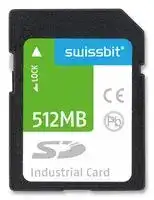


SFSD0512L1BM1TO-I-ME-221-STD
Flash Memory Card, SDHC Card, UHS-1, Class 10, 512 MB, S-450 Series
- Manufacturer: SWISSBIT
- Product type: Flash Memory Cards
- Product Range: S-450 Series
- Memory Capacity: 512MB
- Blank Media Flash Memory Type: SDHC Card, UHS-1, Class 10
| Delivery and price | |
|---|---|
| Units per pack | 50 |
| Price | 24.71 € |
| Current stock | 10+ |
| Lead time | 30 days |
## Product Data Sheet
**Industrial SD / SDHC Memory Card**
**S-450 Series UHS-I Interface, SLC**
Standard and Extended Temperature Grade
Swissbit AG Industriestrasse 4 4. CH-9552 Bronschhofen www.swissbit.com Switzerland industrial@swissbit.com
Revision: 1.21 S-450_data_sheet_SD-LxBM_Rev121
Page 1 of 21
## **Contents**
|**Contents**|**Contents**|
|---|---|
|PRODUCT SUMMARY**....................................................................................................................................................................... 3**||
|1.|ORDERING INFORMATION**...................................................................................................................................................... 4**|
|2.|PRODUCT DESCRIPTION**.......................................................................................................................................................... 5**|
||2.1 PERFORMANCESPECIFICATIONS.................................................................................................................................................. 5|
||2.2 ENVIRONMENTALSPECIFICATIONS............................................................................................................................................... 5|
||2.2.1 Recommended Operating Conditions................................................................................................................ 5|
||2.2.2 Recommended storage conditions................................................................................................................... 6|
||2.2.3 Humidity & EMC................................................................................................................................................... 6|
||2.2.4 Environmental Conditions................................................................................................................................. 6|
||2.3 PHYSICALDIMENSIONS............................................................................................................................................................ 6|
||2.4 RELIABILITY.......................................................................................................................................................................... 7|
|3.|CAPACITY SPECIFICATION**........................................................................................................................................................ 7**|
|4.|CARD PHYSICAL**...................................................................................................................................................................... 8**|
||4.1 PHYSICAL DESCRIPTION............................................................................................................................................................ 8|
|5.|ELECTRICAL INTERFACE**........................................................................................................................................................... 9**|
||5.1 ELECTRICAL DESCRIPTION.......................................................................................................................................................... 9|
||5.2 POWER UP/ POWER DOWN BEAVIOUR AND RESET........................................................................................................................10|
||5.2.1 Power up..............................................................................................................................................................10|
||5.2.2 Power down........................................................................................................................................................10|
||5.2.3 Power drop..........................................................................................................................................................10|
||5.2.4 Operation below minimum voltage................................................................................................................10|
||5.3 DCCHARACTERISTICS..............................................................................................................................................................10|
||5.4 SIGNALLOADING..................................................................................................................................................................10|
||5.5 ACCHARACTERISTICS..............................................................................................................................................................10|
||5.5.1 Default Speed mode (0–25MHz).......................................................................................................................10|
||5.5.2 High Speed mode (0–50MHz)...........................................................................................................................11|
||5.5.3 UHS modes..........................................................................................................................................................11|
|6.|HOST ACCESS SPECIFICATION**.................................................................................................................................................12**|
||6.1 SDANDSPI BUSMODES.......................................................................................................................................................12|
||6.1.1 SD Bus Mode Protocol.........................................................................................................................................12|
||6.1.2 SPI Bus Mode Protocol........................................................................................................................................12|
||6.1.3 Mode Selection....................................................................................................................................................13|
||6.2 CARDREGISTERS...................................................................................................................................................................13|
|7.|PART NUMBER DECODER**.......................................................................................................................................................18**|
||7.1 MANUFACTURER....................................................................................................................................................................18|
||7.2 MEMORYTYPE......................................................................................................................................................................18|
||7.3 PRODUCTTYPE......................................................................................................................................................................18|
||7.4 CAPACITY.............................................................................................................................................................................18|
||7.5 PLATFORM...........................................................................................................................................................................18|
||7.6 GENERATION........................................................................................................................................................................18|
||7.7 MEMORYORGANIZATION.........................................................................................................................................................18|
||7.8 TECHNOLOGY........................................................................................................................................................................18|
||7.9 CHANNELS...........................................................................................................................................................................18|
||7.10 FLASHCODE.......................................................................................................................................................................19|
||7.11 TEMP. OPTION.....................................................................................................................................................................19|
||7.12 DIE CLASSIFICATION.............................................................................................................................................................19|
||7.13 PIN MODE.........................................................................................................................................................................19|
||7.14 CONFIGURATIONXYZ............................................................................................................................................................19|
||7.15 OPTION..............................................................................................................................................................................19|
|8.|SWISSBIT LABEL SPECIFICATION**............................................................................................................................................20**|
||8.1 FRONT SIDE LABEL.................................................................................................................................................................20|
||8.2 BACK SIDE MARKING.............................................................................................................................................................20|
|9.|REVISION HISTORY**.................................................................................................................................................................21**|
|Swissbit AG<br>Revision: 1.21||
|Industriestrasse 4||
|CH-9552 Bronschhofen<br> www.swissbit.com<br> <br>S-450_data_sheet_SD-LxBM_Rev121||
|Switzerland<br> industrial@swissbit.com<br> <br>Page2 of 21||
Revision: 1.21
Page 2 of 21
## **S-450 Series (UHS-I, SLC) Industrial SD / SDHC Memory Card - 512MByte to 32GByte**
## **Product Summary**
- Fully compliant with SD Memory Card specification 3.0
- SD ultra high speed mode, speed class 1 (SDR104)
- SD high speed mode, up to speed class 10
- SD2.0 SDHC backward compliant, default speed and high speed mode
- FAT32 up to 32GB SDHC
- High performance 3.0 specification
- SD burst up to 104MB/s
- SD Normal speed 0…25MHz clock rate
- SD High speed 25…50MHz clock rate
- SD UHS-I speed 0...50MHz (DDR) and 0…208MHz (SDR)
- Up to 90MByte/sec sequential data rate
- Power Supply: (Low-power CMOS technology) `o` 2.7…3.6V normal operating voltage
- Standard SD Memory card form factor
- 32.0mm x 24.0mm x 2.1mm and Write Protect slider
- Optimized FW algorithms especially for high read access and long data retention applications `o` Patented power-off reliability technology
- Wear Leveling technology
- Equal wear leveling of static and dynamic data. The wear leveling assures that dynamic data as well as static data is balanced evenly across the memory. With that the maximum write endurance of the device is guaranteed
- Write Endurance technology
Due to intelligent wear leveling an even use of the entire flash is guaranteed, regardless how much “static” (OS) data is stored.
- Read Disturb Management
The read commands are monitored and the content is refreshed when critical levels have occurred
- Data Care Management
The interruptible background process maintain the user data for Read Disturb effects or Retention degradation due to high temperature effects
- Near miss ECC technology
Minimize the risk of uncorrectable bit failure over the product life time. Each read command analyzes the ECC margin level and refresh data if necessary
- Diagnostic features with Life Time Monitoring tool support
- High reliability
- SLC Flash
- Designed for industrial market especially read intensive application like navigation, infotainment, POS/POI, Medical and general boot medium use case
- The product is optimized for long life cycle that requires good data retention because of high temperature mission profile.
- Intensive write application should use the S-450 Series SLC cards
- Number of card insertions/removals 20,000
- Extended and Industrial Temperature range -25° up to 85°C and -40° up to 85°C, respectively
- SIP (System In Package) process for extreme dust, water and ESD proof
- Selected AEC-Q100 qualification
- Controlled BOM & PCN process
- Manufactured in a TS 16949 certified factory
- Customized options like CID registers, CPRM keys, firmware incl. settings and marking by projects
O87 TALE LE[Teehoo[e]] 8 Joo
Swissbit AG Industriestrasse 4 CH-9552 Bronschhofen Switzerland
Revision: 1.21
www.swissbit.com industrial@swissbit.com
S-450_data_sheet_SD-LxBM_Rev121 Page 3 of 21
## **1. Ordering Information**
## Table 1: Standard Product List
|Capacity|Extended Temperature|Industrial Temperature|
|---|---|---|
||Part Number|Part Number|
|512 MBytes|SFSD0512LgBM1TO-E-ME-2y1-STD|SFSD0512LgBM1TO-I-ME-2y1-STD|
|1 GBytes|SFSD1024LgBM1TO-E-DF-2y1-STD|SFSD1024LgBM1TO-I-DF-2y1-STD|
|2 GBytes|SFSD2048LgBM1TO-E-QG-2y1-STD|SFSD2048LgBM1TO-I-QG-2y1-STD|
|4 GBytes|SFSD4096LgBM1TO-E-ME-2y1-STD|SFSD4096LgBM1TO-I-ME-2y1-STD|
|8 GBytes|SFSD8192LgBM1TO-E-DF-2y1-STD|SFSD8192LgBM1TO-I-DF-2y1-STD|
|16 GBytes|SFSD016GLgBM1TO-E-QG-2y1-STD|SFSD016GLgBM1TO-I-QG-2y1-STD|
|32 GBytes|SFSD032GLgBM1TO-E-NG-2y1-STD|SFSD032GLgBM1TO-I-NG-2y1-STD|
g = product generation and y = firmware revision
Table 2: Available Part Numbers, SLC NAND Flash 24nm
|Capacity|Extended Temperature|Industrial Temperature|
|---|---|---|
||Part Number|Part Number|
|512 MBytes|SFSD0512L1BM1TO-E-ME-221-STD|SFSD0512L1BM1TO-I-ME-221-STD|
|1 GBytes|SFSD1024L1BM1TO-E-DF-221-STD|SFSD1024L1BM1TO-I-DF-221-STD|
|2 GBytes|SFSD2048L1BM1TO-E-QG-221-STD|SFSD2048L1BM1TO-I-QG-221-STD|
|4 GBytes|SFSD4096L1BM1TO-E-ME-221-STD|SFSD4096L1BM1TO-I-ME-221-STD|
|8 GBytes|SFSD8192L1BM1TO-E-DF-221-STD|SFSD8192L1BM1TO-I-DF-221-STD|
|16 GBytes|SFSD016GL1BM1TO-E-QG-221-STD|SFSD016GL1BM1TO-I-QG-221-STD|
|32 GBytes|SFSD032GL1BM1TO-E-NG-221-STD|SFSD032GL1BM1TO-I-NG-221-STD|
Swissbit AG Industriestrasse 4 CH-9552 Bronschhofen Switzerland
Revision: 1.21
www.swissbit.com industrial@swissbit.com
S-450_data_sheet_SD-LxBM_Rev121 Page 4 of 21
## **2. Product Description**
The SD Memory Card is a small form factor non-volatile memory card which provides high capacity data storage. Its aim is to capture, retain and transport data, audio and images, facilitating the transfer of all types of digital information between a large variety of digital systems. The card operates in two basic modes:
- SD/SDHC and UHS-I card modes
- SPI mode
The SD Memory Card also supports SD Default and High Speed mode with up to 50MHz clock frequency as well as UHS-I modes DDR50, SDR12/25/50/104 with up to 208MHz clock frequency. The cards are compliant with
- SD Memory card Specification Part 1, Physical layer Specification V3.01
- SD Memory card Specification Part 2, File System Specification V3.00
- SD Memory card Specification Part 3, Security Specification V3.00
- SD Memory Card Addendum V4.00
## Simplified specifications are available at https://www.sdcard.org/
The SD Card has an internal intelligent controller which manages interface protocols, data storage and retrieval as well as hardware BCH Error Correction Code (ECC), defect handling, diagnostics and clock control. The advanced wear leveling mechanism assures an equal usage of the Flash memory cells to extend the life time.
The hardware BCH-code ECC allows to detect and correct up to 60 defect bits per 1kByte.
The controller performs control read operations and checks the consistence of the data. If an error of some bits is detected, the card refreshes all data in the flash cells to prevent data retention problems.
The card has a power-loss management feature to prevent data corruption after power-down. The cards are RoHS compliant and lead-free.
## **2.1 Performance Specifications**
Table 3: Read/Write Performance
|**2.1 Performance Specifications**<br>Table 3: Read/Write Performance|**2.1 Performance Specifications**<br>Table 3: Read/Write Performance||||
|---|---|---|---|---|
|System Performance(TARGET values)||Typ1 2|Max1|Unit|
|Burst Data transfer Rate(max SD clock 208MHz)|||104|MB/s|
|Sustained Sequential Read|512MB|28|30|MB/s|
||1…2GB|28|34|MB/s|
||4GB|88|90|MB/s|
||8…32GB|88|90|MB/s|
|Sustained Sequential Write|512MB|18|20|MB/s|
||1…2GB|20|24|MB/s|
||4GB|37|40|MB/s|
||8…32GB|73|75|MB/s|
## **2.2 Environmental Specifications**
## 2.2.1 Recommended Operating Conditions
The recommended operating conditions for the S-450 SD Memory Card are provided in Table 4 below.
Table 4: SD Memory Card recommended operating conditions
|Parameter|Min|Typ|Max3|Unit|
|---|---|---|---|---|
|Extended Operating<br>Temperature|-25|25|85|°C|
|Industrial Operating<br>Temperature|-40|25|85|°C|
> 1 All values refer to Toshiba Flash 4Gb or 32Gb
- 2 Sustained Speed measured with USB3.0-SD Memory Card reader in UHS mode. It depends on burst speed, flash number, and file size.
> 3 High Temperature storage without operation reduces the data retention, in operation the data will be refreshed, if data error issues were detected
Swissbit AG Industriestrasse 4 CH-9552 Bronschhofen Switzerland
Revision: 1.21
www.swissbit.com industrial@swissbit.com
S-450_data_sheet_SD-LxBM_Rev121 Page 5 of 21
## 2.2.2 Recommended storage conditions
The recommended storage conditions are listed below in Table 5.
Table 5: SD Memory Card recommended storage conditions
Parameter Min Typ Max[4] Unit Extended Storage Temperature -25 25 100 °C Industrial Operating -40 25 100 °C ~~————~~ Temperature 2.2.3 Humidity & EMC The humidity and EMC conditions are listed below in SD Memory Card recommended storage conditions Table 6.
## Table 6: Humidity & EMC
|Table 6.<br>Table 6: Humidity & EMC||
|---|---|
|Parameter|Condition|
|Humidity (non-condensing)|85% RH @85°C 1000h|
|ESD|up to ±4 kV (contact discharge),<br>according to IEC61000-4-2 and SDA, Human Body Model 150pF/ 330Ohm,<br>on each contact pad, non-operating<br>up to ±15 kV, (air discharge),<br>according to IEC61000-4-2 and SDA, Human Body Model 150pF/ 330Ohm,<br>isolated contact pad area, non-operating|
## 2.2.4 Environmental Conditions
## Table 7: Environmental Conditions
|Parameter|Condition|
|---|---|
|UV light exposure|UV: 254nm, 15Ws/cm<br>2according to ISO7816-1|
|X-Ray|0.1 Gy 70keV to 140KeV (ISO7816-1) according SDA|
|Durability|20,000 mating cycles|
|Drop Test|1.5m free fall|
|Bending / Torque|10N / 0.15Nm ±2.5° max|
|Mechanical Shock|1500G, 0.5ms, half sine wave ±xyz-axis, 4 pulses each<br>non-operating, JESD22B110/B104 Condition B|
|Vibration|50G, p-p, 20..2000Hz, sweep xyz-axis,<br>4 pulses each, non-operating, MIL-STD-883 M2007.3 Condition B|
## **2.3 Physical Dimensions**
The physical dimensions of the S-450 SD Memory Card are listed in the following table.
Table 8: Physical Dimensions
|Table 8: Physical Dimensions|||
|---|---|---|
|Outer Physical Dimensions|Value|Unit|
|Length|32.00±0.1|mm|
|Width|24.00±0.1|mm|
|Thickness|2.10±0.15|mm|
|Weight (typ.)|2|g|
> 4 High Temperature storage without operation reduces the data retention, in operation the data will be refreshed, if data error issues were detected Swissbit AG Industriestrasse 4 CH-9552 Bronschhofen www.swissbit.com Switzerland
Revision: 1.21
www.swissbit.com industrial@swissbit.com
S-450_data_sheet_SD-LxBM_Rev121 Page 6 of 21
## **2.4 Reliability** Table 9: Reliability
|**2.4 Reliability**<br>Table 9: Reliability||
|---|---|
|Parameter|Value5|
|Data Retention at beginning @ 40°C|10 years|
|Data Retention at life end (100k PE cycles) @ 40°C|1 year|
## **3. Capacity specification**
## Table 10: SD Memory Card capacity specification
|Capacity|Sector|Total Addressable Bytes|
|---|---|---|
|512MB|967,680|495,452,160|
|1GB|1,953,792|1,000,341,504|
|2GB|3,938,304|2’016’411,648|
|4GB|7,774,208|3,980,394,496|
|8GB|15,802,368|8,090,812,416|
|16GB|31,834,112|16,299,065,344|
|32GB|62,333,952|31,914,983,424|
> 5 After every power on the card reads the whole flash and performs a data refresh if necessary. So, the data retention can be much longer in most use cases. Swissbit AG Industriestrasse 4 CH-9552 Bronschhofen www.swissbit.com Switzerland
Revision: 1.21
www.swissbit.com industrial@swissbit.com
S-450_data_sheet_SD-LxBM_Rev121 Page 7 of 21
## **4. Card physical**
## **4.1 Physical description**
The SD Memory Card contains a single chip controller and Flash memory module(s). The controller interfaces with a host system allowing data to be written to and read from the Flash memory module(s).
Figure 1: Simplified mechanical dimensions SD Memory Card
Swissbit AG Industriestrasse 4 CH-9552 Bronschhofen Switzerland
Revision: 1.21
www.swissbit.com industrial@swissbit.com
S-450_data_sheet_SD-LxBM_Rev121 Page 8 of 21
## **5. Electrical interface**
## **5.1 Electrical description**
Figure 2: SD Memory Card Shape and Interface (Top View)
– Table 11: Pad Assignemnt SD Mode
|Table 11: Pad Assignemnt|Table 11: Pad Assignemnt–SD Mode|Table 11: Pad Assignemnt–SD Mode|Table 11: Pad Assignemnt–SD Mode|
|---|---|---|---|
|Pin|SD Mode|||
||Name|Type6|Description|
|1|CD/DAT37|I/O/PP8|Card Detect/ Data Line [Bit 3]|
|2|CMD|PP|Command/Response|
|3|VSS1|S|Supply voltage ground|
|4|VDD|S|Supply voltage|
|5|CLK|I|Clock|
|6|VSS2|S|Supply voltage ground|
|7|DAT0|I/O/PP|Data Line [Bit 0]|
|8|DAT19|I/O/PP|Data Line [Bit 1]|
|9|DAT210|I/O/PP|Data Line [Bit 2]|
– Table 12: Pad Assignment SPI Mode
|Table 12: Pad Assignment|Table 12: Pad Assignment–SPI Mode|Table 12: Pad Assignment–SPI Mode|Table 12: Pad Assignment–SPI Mode|
|---|---|---|---|
|Pin|SPI Mode|||
||Name|Type6|Description|
|1|CS|I8|Chip Select (neg true)|
|2|DI|I|Data In|
|3|VSS|S|Supply voltage ground|
|4|VDD|S|Supply voltage|
|5|SCLK|I|Clock|
|6|VSS2|S|Supply voltage ground|
|7|DO|O/PP|Data Out|
|8|RSV|||
|9|RSV|||
> 6 S: power supply; I: input; O: output using push-pull drivers; PP: I/O using push-pull drivers
> 7 The extended DAT lines (DAT1-DAT3) are input on power up. They start to operate as DAT lines after SET_BUS_WIDTH command. The Host shall keep its own DAT1-DAT3 lines in input mode, as well, while they are not used.
> 8 At power up this line has a 50kOhm pull up enabled in the card. This resistor serves two functions Card detection and Mode Selection. For Mode Selection, the host can drive the line high or let it be pulled high to select SD mode. If the host wants to select SPI mode it should drive the line low. For Card detection, the host detects that the line is pulled high. This pull-up should be disconnected by the user, during regular data transfer, with SET_CLR_CARD_DETECT (ACMD42) command
> 9 DAT1 line may be used as Interrupt Output (from the Card) in SDIO mode during all the times that it is not in use for data transfer operations (refer to "SDIO Card Specification" for further details).
> 10 DAT2 line may be used as Read Wait signal in SDIO mode (refer to "SDIO Card Specification" for further details).
Swissbit AG Industriestrasse 4 CH-9552 Bronschhofen Switzerland
Revision: 1.21
www.swissbit.com industrial@swissbit.com
S-450_data_sheet_SD-LxBM_Rev121 Page 9 of 21
## **5.2 Power up / Power down beaviour and reset**
## 5.2.1 Power up
When the voltage is ramped up the controller is ready (internal reset pin released) if the voltage reaches 1.65V. The host can start with communication 1ms after 2.7V is reached according the SDA soecification. That should perform 74 clock cycles and start with the sequence CMD0, CMD8, ACMD41 until card is ready as described in the SD specification 3.01.
## 5.2.2 Power down
When the power falls below 2.6V the controller stopps the communication to the flash, but enables the flash to finish a started flash program operation (if voltage drop is not fast).
After next initialization the controller checks the last written data for consistency and refreshs the data. Either the new or the old data (if the write operation could not be finished) are available.
## 5.2.3 Power drop
If the voltage drops below 2.6V and rises again, the card performes a reset. The card must be initialized like after a power on.
## 5.2.4 Operation below minimum voltage
If the card initialization is perfomed below the specified voltage of 2.7V, the card may be detected as 1MB card with no usefull data. In this case the host should power off and on the card and start initialization above 2.7V.
## **5.3 DC characteristics**
Measurements are at Recommended Operating Conditions unless otherwise specified.
Table 13: DC Characteristics
|Table 13: DC Characteristics|Table 13: DC Characteristics||||||
|---|---|---|---|---|---|---|
|Symbol<br>~~TT~~|Parameter<br>~~TT~~|Min<br>~~TT~~|Typ<br>~~TT~~|Max<br>~~TT~~|Unit<br>~~TT~~|Notes<br>~~TT~~|
|IDD<br>~~OO~~|Operating Current Read<br>~~OO~~|~~OO~~|60<br>~~OO~~|120<br>~~OO~~|mA<br>~~OO~~|@ 25°C<br>~~OO~~|
|IDD<br>~~OO~~|Operating Current Write<br>~~OO~~|~~OO~~|70<br>~~OO~~|120<br>~~OO~~|mA<br>~~OO~~|@ 25°C<br>~~OO~~|
|IDD<br>~~OO~~|Background read and refresh11<br>~~OO~~|~~OO~~|80<br>~~OO~~|120<br>~~OO~~|mA<br>~~OO~~|@ 25°C<br>~~OO~~|
|IDD<br>~~a~~|Pre-initialization Standby Current<br>~~GO~~|~~GO~~|5<br>~~GO~~|15<br>~~GO~~|mA<br>~~GO~~|@ 25°C<br>~~GO~~|
|IDD<br>~~a~~|Post-initialization StandbyCurrent12<br>~~GO~~|~~GO~~|2<br>~~GO~~|9<br>~~GO~~|mA<br>~~GO~~|@ 25°C<br>~~GO~~|
|IDD<br>~~a~~|Post-initialization StandbyCurrent12<br>~~GO~~|~~GO~~|5<br>~~GO~~|15<br>~~GO~~|mA<br>~~GO~~|@ 85°C<br>~~GO~~|
|ILI<br>~~a~~|Input Leakage Current<br>~~GO~~|-2<br>~~GO~~|~~GO~~|2<br>~~GO~~|µA<br>~~GO~~|without pull up R<br>~~GO~~|
|ILO<br>~~CC~~|Output Leakage Current<br>~~CC~~|-2<br>~~CC~~|~~CC~~|2<br>~~CC~~|µA<br>~~CC~~|without pull up R<br>~~CC~~|
## **5.4 Signal Loading**
According to SD specification
## **5.5 AC characteristics**
## 5.5.1 Default Speed mode (0–25MHz)
According to SD specification
> 11 The card can perform auto data read of the whole card to check for ECC errors and performs data refresh
> 12 Before auto read the idle current is larger than the typical idle current after auto read
www.swissbit.com
Swissbit AG Industriestrasse 4 CH-9552 Bronschhofen Switzerland
Revision: 1.21
S-450_data_sheet_SD-LxBM_Rev121 Page 10 of 21
industrial@swissbit.com
## 5.5.2 High Speed mode (0–50MHz)
According to SD specification
## 5.5.3 UHS modes
UHS modes were driven with a signal level of 1.8V. The cards support following UHS-I modes:
- Table 15: Supported UHS I modes
|Table 15: Supported UHS-I modes|I modes||
|---|---|---|
|Mode|Max. Burst MB/s|Max. Clock frequencyMHz|
|SDR12|12.5|25|
|SDR25|25|50|
|SDR50|50|100|
|SDR104|104|208|
|DDR50|50|50(risingand fallingedge)|
According to SD specification
Swissbit AG Industriestrasse 4 CH-9552 Bronschhofen Switzerland
Revision: 1.21
www.swissbit.com industrial@swissbit.com
S-450_data_sheet_SD-LxBM_Rev121 Page 11 of 21
## **6. Host access Specification**
The following chapters summarize how the host accesses the card:
- Chapter 6.1 summarizes the SD and SPI buses.
- Chapter 6.2 summarizes the registers.
## **6.1 SD and SPI Bus Modes**
The card supports SD and the SPI Bus modes. Application can chose either one of the modes. Mode selection is transparent to the host. The card automatically detects the mode of the reset command and will expect all further communication to be in the same communication mode. The SD mode uses a 4-bit high performance data transfer, and the SPI mode provides compatible interface to MMC host systems with little redesign, but with a lower performance.
## 6.1.1 SD Bus Mode Protocol
The SD Bus mode has a single master (host) and multiple slaves (cards) synchronous topology. Clock, power, and ground signals are common to all cards. After power up, the SD Bus mode uses DAT0 only; after initialization, the host can change the cards’ bus width from 1 bit (DAT0) to 4 bits (DAT0-DAT3). In high speed mode, only one card can be connected to the bus.
Communication over the SD bus is based on command and data bit streams which are initiated by a start bit and terminated by a stop bit.
- Command: a command is a token which starts an operation. A command is sent from the host either to a single card (addressed command) or to all connected cards (broadcast command). A command is transferred serially on the CMD line.
- Response: a response is a token which is sent from an addressed card, or (synchronously) from all connected cards, to the host as an answer to a previously received command. A response is transferred serially on the CMD line.
- Data: data can be transferred from the card to the host or vice versa. Data is transferred via the data lines.
## 6.1.2 SPI Bus Mode Protocol
The Serial Parallel Interface (SPI) Bus is a general purpose synchronous serial interface. The SPI mode consists of a secondary communication protocol. The interface is selected during the first reset command after power up (CMD0) and it cannot be changed once the card is powered on.
While the SD channel is based on command and data bit streams which are initiated by a start bit and terminated by a stop bit, the SPI channel is byte oriented. Every command or data block is built of 8-bit bytes and is byte aligned to the CS signal.
The card identification and addressing methods are replaced by a hardware Chip Select (CS) signal. There are no broadcast commands. For every command, a card (slave) is selected by asserting (active low) the CS signal.
The CS signal must be continuously active for the duration of the SPI transaction (command, response and data). The only exception occurs during card programming, when the host can de-assert the CS signal without affecting the programming process.
The bidirectional CMD and DAT lines are replaced by unidirectional dataIn and dataOut signals.
Table 16: SPI Bus Signals
|Signal|Description|
|---|---|
|/CS|Host to card chipselect|
|CLK|Host to card clock signal|
|Data In|Host to card data signal|
|Data Out|Card to host data signal|
|Vdd,Vss|Power andground|
Swissbit AG Industriestrasse 4 CH-9552 Bronschhofen Switzerland
Revision: 1.21
www.swissbit.com industrial@swissbit.com
S-450_data_sheet_SD-LxBM_Rev121 Page 12 of 21
## 6.1.3 Mode Selection
The SD Memory Card wakes up in the SD mode. It will enter SPI mode if the CS signal is asserted (negative) during the reception of the reset command (CMD0) and the card is in idle_state. If the card recognizes that the SD mode is required it will not respond to the command and remain in the SD mode.
If SPI mode is required the card will switch to SPI and respond with the SPI mode R1 response. The only way to return to the SD mode is by entering the power cycle. In SPI mode the SD Memory Card protocol state machine is not observed. All the SD Memory Card commands supported in SPI mode are always available.
During the initialization sequence, if the host gets Illegal Command indication for ACMD41 sent to the card, it may assume that the card is Multimedia Card. In that case it should re-start the card as Multimedia Card using CMD0 and CMD1.
## **6.2 Card Registers**
The SD Memory Card has the following registers.
Table 17: SD Memory Card registers
|Register name|Bit width|Description|Function|
|---|---|---|---|
|CID|128|Card Identification<br>information|This register contains the card identification information<br>used duringthe Card Identificationphase.|
|OCR|32|Operation Conditions<br>Registers|This register describes the operating voltage range and<br>contains the status bit in thepower supply.|
|CSD|128|Card specific information|This register provides information on how to access the card<br>content. Some fields of this register are writeable by<br>PROGRAM_CSD(CMD27).|
|SCR|64|SD Memory Card’s Special<br>features|This register provides information on special features.|
|RCA13|16|Relative Card Address|This register carries the card address is SD Card mode.|
|SSR|512|SD Status|information about the card proprietary features and vendor<br>specific life time information|
Table 18: CID register
|Table 18: CID register||||
|---|---|---|---|
|Register name|Bit Width|Description|Function|
|MID|8|Manufacture ID|0x5d|
|OID|16|OEM/Application ID|0x5342|
|PNM|40|Product Name|(“LgBM1”)<br>g=generation|
|PRV|8|Product Revision|0xgg|
|PSN|32|Product Serial Number|xxxxxxxx|
|—|4|Reserved|0x0|
|MDT|12|Manufacture Date|0xyym|
|CRC|7|Check sum of CID contents|chksum|
|—|1|Not used; always=1|1|
> 13 RCA register is not available in SPI mode
Swissbit AG Industriestrasse 4 CH-9552 Bronschhofen Switzerland
Revision: 1.21
www.swissbit.com industrial@swissbit.com
S-450_data_sheet_SD-LxBM_Rev121 Page 13 of 21
Table 19: OCR register
|~~a~~|~~ee~~|~~ee~~|~~ee~~|~~ee~~||
|---|---|---|---|---|---|
|OCR bit positon<br>~~a~~|VDD voltage<br>windows<br>~~ee~~|Typ. value<br>~~ee~~|OCR bit<br>position<br>~~ee~~|VDD voltage window<br>~~ee~~|Typ. value|
|0-3<br>~~a~~<br>~~Ca~~|Reserved<br>~~ee~~<br>~~Ca~~|0<br>~~ee~~<br>~~a~~|15<br>~~ee~~|2.7-2.8<br>~~ee~~|1|
|4<br>~~Ca~~<br>~~I~~|1.6-1.7<br>~~Ca~~<br>~~I~~|0<br>~~a~~<br>~~I~~|16<br>~~I~~|2.8-2.9<br>~~I~~|1<br>~~I~~|
|5<br>~~I~~<br>~~a~~|1.7-1.8<br>~~I~~<br>~~a~~|0<br>~~I~~<br>~~a~~<br>~~a~~|17<br>~~I~~<br>~~a~~<br>~~a~~|2.9-3.0<br>~~I~~<br>~~a~~<br>~~a~~|1<br>~~I~~<br>~~a~~<br>~~a~~|
|6<br>~~a~~<br>~~I~~|1.8-1.9<br>~~a~~<br>~~I~~|0<br>~~a~~<br>~~a~~<br>~~I~~|18<br>~~a~~<br>~~a~~<br>~~I~~|3.0-3.1<br>~~a~~<br>~~a~~<br>~~I~~|1<br>~~a~~<br>~~a~~<br>~~I~~|
|7<br>~~I~~<br>~~a~~|1.9-2.0<br>~~I~~<br>~~a~~|0<br>~~I~~<br>~~a~~<br>~~OO~~|19<br>~~I~~<br>~~a~~<br>~~OO~~|3.1-3.2<br>~~I~~<br>~~a~~<br>~~OO~~|1<br>~~I~~<br>~~a~~<br>~~OO~~|
|8<br>~~a~~<br>~~|~~<br>~~a~~|2.0-2.1<br>~~a~~<br>~~|~~<br>~~a~~|0<br>~~a~~<br>~~OO~~<br>~~|~~<br>~~Oa~~|20<br>~~a~~<br>~~OO~~<br>~~|~~|3.2-3.3<br>~~a~~<br>~~OO~~<br>~~|~~|1<br>~~a~~<br>~~OO~~<br>~~|~~|
|9<br>~~|~~<br>~~a~~<br>~~a~~|2.1-2.2<br>~~|~~<br>~~a~~<br>~~a~~|0<br>~~|~~<br>~~a~~<br>~~Oa~~|21<br>~~|~~<br>~~a~~|3.3-3.4<br>~~|~~<br>~~a~~|1<br>~~|~~<br>~~a~~|
|10<br>~~a~~|2.2-2.3<br>~~a~~|0<br>~~Oa~~|22|3.4-3.5|1|
|11<br>~~a~~<br>|2.3-2.4<br>~~a~~<br>~~ae~~|0<br>~~ee~~|23<br>~~ee~~|3.5-3.6<br>~~ee~~|1|
|12<br>~~a~~|2.4-2.5<br>~~aae~~|0<br>~~ee~~|24<br>~~ee~~|Switching to 1.8V<br>accepted<br>~~ee~~|1|
|13<br><br>~~a~~|2.5-2.6<br>~~ae~~<br>~~a~~|0<br>~~ee~~|25-29<br>~~ee~~|Reserved<br>~~ee~~||
|14<br>~~OO~~|2.6-2.7<br>~~OO~~|0<br>~~OO~~|30<br>~~OO~~|Card Capacity Status (CCS)<br>~~OO~~|*14<br>~~OO~~|
|~~OO~~<br>~~sO~~|~~OO~~<br>~~sO ~~|~~OO~~<br> ~~OO~~|31<br>~~OO~~<br>~~OO~~|0=busy; 1=ready<br>~~OO~~<br>~~OO~~|*15<br>~~OO~~<br>~~OO~~|
> 14 This bit is valid only when the card power up status bit is set
> 15 This bit is set to LOW if the card has not finished the power up routine
Swissbit AG Industriestrasse 4 CH-9552 Bronschhofen Switzerland
Revision: 1.21
www.swissbit.com industrial@swissbit.com
S-450_data_sheet_SD-LxBM_Rev121 Page 14 of 21
## Table 20: CSD register
|Table 20: CSD register<br>~~ee~~|~~es~~|~~ee~~||SUIISSDIt|
|---|---|---|---|---|
|Register Name<br>~~ee~~|Bits<br>~~es~~|Bit Width<br>~~ee~~|Description|Typ. Value<br>SDHC|
|CSD_STRUCTURE<br>~~ee ~~|127:126<br> ~~es ~~|2<br> ~~ee~~|CSD structure|01|
|—<br>~~OO~~|125:120<br>~~OO~~|6<br>~~OO~~|Reserved<br>~~OO~~|00000<br>~~OO~~|
|TAAC<br>~~TT~~|119:112<br>~~TT~~|8<br>~~TT~~|Data read access time 1<br>~~TT~~|00001110<br>~~TT~~|
|NSAC<br>~~TT~~<br>~~ee~~<br>~~To~~|111:104<br>~~TT~~<br>~~ee~~|8<br>~~TT~~<br>~~ee~~|Data read access time 2 (CLK cycle)<br>~~TT~~<br>~~ee~~|00000000<br>~~TT~~<br>~~ee~~<br>~~ee~~|
|TRAN_SPEED<br>~~ee~~<br>~~To~~|103:96<br>~~ee~~|8<br>~~ee~~|Data transfer rate<br>~~ee~~|00110010 Default speed<br>00101011 SDR 104<br>or other values<br>~~ee~~<br>~~ee~~|
|CCC<br>~~ee ~~<br>~~To~~|95:84<br> ~~ee~~|12<br>~~ee~~|Card command classes<br>~~ee~~|010110110101<br>~~ee~~<br>~~ee~~|
|READ_BL_LEN<br>~~To~~<br>~~TT~~|83:80<br>~~TT~~|4<br>~~TT~~|Read data block length<br>~~TT~~|1001<br>~~ee~~<br>~~TT~~|
|READ_BL_PARTIAL<br>~~OO~~|79<br>~~OO~~|1<br>~~OO~~|Partial blocks for read allowed<br>~~OO~~|0<br>~~OO~~|
|WRITE_BLK_MISALIGN<br>~~TP~~|78<br>~~TP~~|1<br>~~TP~~|Write block misalignment<br>~~TP~~|0<br>~~TP~~|
|READ_BLK_MISALIGN<br>~~TP~~|77<br>~~TP~~|1<br>~~TP~~|Read block misalignment<br>~~TP~~|0<br>~~TP~~|
|DSR_IMP<br>~~I~~|76<br>~~I~~|1<br>~~I~~|DSR implemented<br>~~I~~|0<br>~~I~~|
|—<br>~~TP~~|75:70<br>~~TP~~|6<br>~~TP~~|Reserved<br>~~TP~~|000000<br>~~TP~~|
|C_SIZE<br>~~TP~~|69:48<br>~~TP~~|22<br>~~TP~~|Device size<br>~~TP~~|xxx16<br>~~TP~~|
|—<br>~~I~~|47<br>~~I~~|1<br>~~I~~|Reserved<br>~~I~~|0<br>~~I~~|
|ERASE_BLK_EN<br>~~OO~~<br>~~To~~|46<br>~~OO~~|1<br>~~OO~~|Erase single block enable<br>~~OO~~|1<br>~~OO~~|
|SECTOR_SIZE<br>~~To~~|45:39|7|Erase sector size|1111111|
|WP_GRP_SIZE<br>~~To~~|38:32|7|Write protect group size|0000000|
|WP_GRP_ENABLE<br>~~TT~~<br>~~To~~|31<br>~~TT~~|1<br>~~TT~~|Write protect group enable<br>~~TT~~|0<br>~~TT~~|
|—<br>~~To~~|30:29|2|Reserved|00|
|R2W_FACTOR<br>~~To~~|28:26|3|Write speed factor|010|
|WRITE_BL_LEN<br>~~TT~~|25:22<br>~~TT~~|4<br>~~TT~~|Write data block length<br>~~TT~~|100116<br>~~TT~~|
|WRITE_BL_PARTIAL<br>~~OO~~<br>~~To~~|21<br>~~OO~~|1<br>~~OO~~|Partial blocks for write allowed<br>~~OO~~|0<br>~~OO~~|
|—<br>~~To~~|20:16|5|Reserved|00000|
|FILE_FORMAT_GRP<br>~~To~~<br>~~TT~~|15<br>~~TT~~|1<br>~~TT~~|File format group<br>~~TT~~|0 W(1)<br>~~TT~~|
|COPY<br>~~OO~~|14<br>~~OO~~|1<br>~~OO~~|Copy flag<br>~~OO~~|0 W(1)<br>~~OO~~|
|PERM_WRITE_PROTECT<br>~~TP~~|13<br>~~TP~~|1<br>~~TP~~|Permanent write protection<br>~~TP~~|0 W(1)<br>~~TP~~|
|TMP_WRITE_PROTECT<br>~~nT~~|12<br>~~nT~~|1<br>~~nT~~|Temporary write protection<br>~~nT~~|0 W<br>~~nT~~|
|FILE_FORMAT<br>~~TT~~|11:10<br>~~TT~~|2<br>~~TT~~|File format<br>~~TT~~|00 W(1)<br>~~TT~~|
|—<br>~~OO~~<br>~~To~~|9:8<br>~~OO~~<br>|2<br>~~OO~~<br>|Reserved<br>~~OO~~<br>|00 W<br>~~OO~~<br>|
|CRC<br>~~To~~|7:1<br>|7<br>|Checksum of CSD contents<br>|xxxxxxx W<br>|
|—<br>~~ToI~~|0<br>~~I~~|1<br>~~I~~|Always=1<br>~~I~~|1<br>~~I~~|
Memory capacity = (C_SIZE+1) * 512kByte
W value can be changed with CMD27 (PROGRAM_CSD)
W(1) value can be changed ONCE with CMD27 (PROGRAM_CSD)
> 16 Drive size and block sizes vary with card capacity
Swissbit AG Industriestrasse 4 CH-9552 Bronschhofen Switzerland
Revision: 1.21
www.swissbit.com
S-450_data_sheet_SD-LxBM_Rev121 Page 15 of 21
industrial@swissbit.com
Table 21: SCR register
**==> picture [504 x 223] intentionally omitted <==**
**----- Start of picture text -----**<br>
|||||||||
|---|---|---|---|---|---|---|---|
|Table 21: SCR register|
|Or|Field|Bits|Bit Width|Or|typ Value|F Nn”.|remark|
|OG|SCR_STRUCTURE|63:60|4|0000|SCR 1.01…2.00|
|Wo|SD_SPEC|59:56|4|J|0010|SD 2.0 or 3.0|
|SG|DATA_STAT_AFTER_ERASE|55|1|1|data are 0xFF after erase|
|SD_SECURITY|54:52|3|011|2.00 (SDHC)|
|TF|oe|
|OG|SD_BUS_WIDTHS|51:48|4|0101|1 or 4 bit|
|Wo|SD_SPEC3|47|1|1|yes||SD3.0|
|TF|EX_SECURITY|46:43|4|Joe|0000|no extended security|
|Reserved|42:34|9|0|0|
|OG|
|J|CMD_SUPPORT|33:32|2|11|CMD23 and CMD20 supported|
|Reserved|31:0|32|0|0|
|TT|So||
|Table 22: RCA register|
|Field|Bits|Bit width|
|RCA|16|0x0000|[17]|
**----- End of picture text -----**<br>
> 17 After initialization the card can change the RCA register
Swissbit AG Industriestrasse 4 CH-9552 Bronschhofen Switzerland
Revision: 1.21
www.swissbit.com industrial@swissbit.com
S-450_data_sheet_SD-LxBM_Rev121 Page 16 of 21
Table 23: SSR register
|Table 23: SSR register|||||
|---|---|---|---|---|
|Field<br>~~a~~|Bits|Bit Width|Bit Width<br>typ Value|remark|
|Data bus width<br>~~eG~~|511:510<br>~~eG~~|2<br>~~eG~~|0x218<br>~~eG~~|4 bit width<br>~~eG~~|
|Secured mode<br>~~a~~|509:509<br>~~a~~|1<br>~~a~~|0x0<br>~~a~~|not secured<br>~~a~~|
|Reserved for security<br>~~a~~<br>~~a~~|508:502<br>~~a~~<br>~~a~~|7<br>~~a~~<br>~~a~~|0x00<br>~~a~~<br>~~a~~|-<br>~~a~~<br>~~a~~|
|Reserved<br>~~a~~<br>~~a~~|501:496<br>~~a~~<br>~~a~~|6<br>~~a~~<br>~~a~~|0x00<br>~~a~~<br>~~a~~|-<br>~~a~~<br>~~a~~|
|SD card type|495:480<br>~~ee~~|16<br>~~ee~~|0x0000<br>~~ee~~|Regular SD<br>~~ee~~|
|Size protected area<br>~~ee~~|479:448<br>~~ee~~<br>~~ee~~|32<br>~~ee~~<br>~~ee~~|0x03000000<br>0x04000000<br>0x05000000<br>~~ee~~<br>~~ee~~|48MB<br>64MB<br>80MB<br>~~ee~~<br>~~ee~~|
|Speed class<br>~~eG~~<br>~~a~~|447:440<br>~~ee ~~<br>~~eG~~<br>|8<br> ~~ee~~<br>~~eG~~<br>|0x04<br>~~ee~~<br>~~eG~~<br>|Class 10<br>~~ee~~<br>~~eG~~<br>|
|Move performance<br>~~a~~|439:432<br>|8<br>|0x05<br>0x00<br>|5 MB/s<br>sequential write<br>|
|Allocation unit size<br>~~aa~~|431:428<br>~~a~~|4<br>~~a~~|0x8<br>~~a~~|2 MiB<br>~~a~~|
|Reserved<br>~~a~~<br>~~a~~|427:424<br>~~a~~<br>~~a~~|4<br>~~a~~<br>~~a~~|0x0<br>~~a~~<br>~~a~~|~~a~~<br>~~a~~|
|Erase unit size<br>~~a~~<br>~~a~~|423:408<br>~~a~~<br>~~a~~|16<br>~~a~~<br>~~a~~|0x0001<br>~~a~~<br>~~a~~|1 AU<br>~~a~~<br>~~a~~|
|Erase unit timeout<br>~~a~~|407:402<br>~~a~~|6<br>~~a~~|0x10<br>~~a~~|16 seconds<br>~~a~~|
|Erase unit offset<br>~~a~~<br>~~a~~|401:400<br>~~a~~<br>~~a~~|2<br>~~a~~<br>~~a~~|0x1<br>~~a~~<br>~~a~~|1 seconds<br>~~a~~<br>~~a~~|
|UHS mode Speed Grade<br>~~a~~<br>~~a~~|399:396<br>~~a~~<br>~~a~~|4<br>~~a~~<br>~~a~~|0x1<br>~~a~~<br>~~a~~|10MB/s and above<br>~~a~~<br>~~a~~|
|Allocation unit size in UHS mode<br>~~eG~~|395:392<br>~~eG~~|4<br>~~eG~~|0x8<br>~~eG~~|2 MiB<br>~~eG~~|
|Reserved<br>~~a~~|391:312<br>~~a~~|80<br>~~a~~|~~a~~|~~a~~|
|Data structure version identifier, currently 1<br>~~a~~<br>~~a~~|311:304<br>~~a~~<br>~~a~~|8<br>~~a~~<br>~~a~~|0x01<br>~~a~~<br>~~a~~|version 1<br>~~a~~<br>~~a~~|
|Number of manufacturer marked defect blocks<br>~~a~~<br>~~a~~|303:288<br>~~a~~<br>~~a~~|16<br>~~a~~<br>~~a~~|0x0046<br>~~a~~<br>~~a~~|70 initial BB<br>~~a~~<br>~~a~~|
|Number of initial spare blocks (worst chip)<br>~~a~~|287:272<br>~~a~~|16<br>~~a~~|0x00b9<br>~~a~~|185 spare blocks<br>~~a~~|
|Number of initial spare blocks (sum over all chips)<br>~~a~~<br>~~a~~|271:256<br>~~a~~<br>~~a~~|16<br>~~a~~<br>~~a~~|0x033e<br>~~a~~<br>~~a~~|830 spare blocks<br>~~a~~<br>~~a~~|
|Percentage of remaining spare blocks (worst chip)<br>~~a~~<br>~~a~~|255:248<br>~~a~~<br>~~a~~|8<br>~~a~~<br>~~a~~|0x6418<br>~~a~~<br>~~a~~|100%<br>~~a~~<br>~~a~~|
|Percentage of remaining spare blocks (all chips)<br>~~eG~~<br>~~a~~|247:240<br>~~eG~~|8<br>~~eG~~|0x6418<br>~~eG~~|100%<br>~~eG~~|
|Number of uncorrectable ECC errors (not including ECC<br>errors during startup)<br>~~a~~<br>~~**a**~~|239:224|16|0x000018|0 uncorrectable errors|
|Number of correctable ECC errors (not including ECC<br>errors during startup)<br>~~a~~<br>~~**a**~~|223:192|32|0x0045074b18|4523851 correctable ECC<br>errors|
|Lowest wear level class<br>~~**a**~~|191:176|16|0x000018|0|
|Highest wear level class<br>~~a~~<br>~~a~~|175:160<br>~~a~~|16<br>~~a~~|0x000018<br>~~a~~|0<br>~~a~~|
|Wear level threshold<br>~~a~~<br>~~a~~|159:144|16|0x03ff|1024 block erases per WL<br>class|
|Total number of block erases<br>~~a~~<br>~~a~~|143:96|48|0x00…22307218|224026 block erase<br>commands|
|Number of flash blocks, in units of 256 blocks<br>~~a~~<br>~~a~~|95:80|16|0x0040|16384 flash blocks|
|Maximum flash block erase count target, in wear level<br>class units<br>~~es~~|79:64<br>~~es~~|16<br>~~es~~|0x00xx<br>~~es~~|Flash endurance xx WL<br>classes<br>~~es~~|
|Power on count<br>~~a~~|63:32<br>~~a~~|32<br>~~a~~|0x0000000318<br>~~a~~|3x power on<br>~~a~~<br>~~FrNn—”—__~~|
|Firmware version<br>~~She~~|31:0<br>~~She~~|32<br>~~She~~|0xYYMMDDXX<br>~~She~~|Firmware Version<br>~~She~~<br>~~FrNn—”—__~~|
Bit 311:0 are vendor specific, example values in the table
> 18 Value change in operation
Swissbit AG Industriestrasse 4 CH-9552 Bronschhofen Switzerland
Revision: 1.21
www.swissbit.com industrial@swissbit.com
S-450_data_sheet_SD-LxBM_Rev121 Page 17 of 21
**7. Part Number Decoder** S F SD 016G L 1 B M 1 TO - I - Q G - 221 - STD 1 2 3 4 5 6 7 8 9 10 11 12 13 14 15 Manuf. Option Memory Type. Configuration Product Type Manuf. Code: Flash Mode Density Manuf. Code: Flash Package Platform Temp. Option Product Generation Flash vendor Code Memory Organization Channels ~~TITEL~~ Technology **7.1 Manufacturer** Swissbit code S **7.2 Memory Type**
|Swissbit code|S|
|---|---|
|||
|Flash|F|
## **7.3 Product Type**
SD Memory Card SD 256 MByte 0256 512 MByte 0512 1 GByte 1024 2 GByte 2048 4 GByte 4096 8 GByte 8192 16 GByte 016G 32 GByte 032G ~~a~~ SD Memory Card L 1 Generation 2 x8 B SD Memory Card controller S-4xx Platform M 1 Flash Channel 1
## **7.4 Capacity**
## **7.5 Platform**
## **7.6 Generation**
## **7.7 Memory Organization**
## **7.8 Technology**
## **7.9 Channels**
Swissbit AG Industriestrasse 4 CH-9552 Bronschhofen Switzerland
Revision: 1.21
www.swissbit.com
S-450_data_sheet_SD-LxBM_Rev121 Page 18 of 21
industrial@swissbit.com
## **7.10 Flash Code**
## **7.11 Temp. Option**
Toshiba TO Extended Temp. Range - ° ° E 25 C to 85 C Industrial Temp. Range - ° ° I ~~——~~ 40 C to 85 C
**7.12 DIE Classification** S-450 SLC MONO (single die package) M DDP (dual die package) D QDP (quad die package) Q ~~=——=~~ ODP (octal die package) N **7.13 PIN Mode** Single nCE & R/nB E Dual nCE & Dual R/nB F ~~—=~~ Quad nCE & Quad R/nB G **7.14 Configuration XYZ** X Configuration Configuration X default, non UHS 1 UHS-I 2 ~~—~~ Y FW Revision FW Revision Y Version 1 1 Version 2 2 ~~—~~ Z optional Optional Z ~~TT~~ optional 1 **7.15 Option** Swissbit / Standard STD
Swissbit AG Industriestrasse 4 CH-9552 Bronschhofen Switzerland
Revision: 1.21
www.swissbit.com
S-450_data_sheet_SD-LxBM_Rev121 Page 19 of 21
industrial@swissbit.com
## **8. Swissbit Label specification**
## **8.1 Front side label**
512MB SD
1GB SD
2GB SD
**==> picture [45 x 9] intentionally omitted <==**
**----- Start of picture text -----**<br>
4GB SDHC<br>**----- End of picture text -----**<br>
8GB SDHC 16GB SDHC
**==> picture [49 x 9] intentionally omitted <==**
**----- Start of picture text -----**<br>
32GB SDHC<br>**----- End of picture text -----**<br>
## **8.2 Back side marking**
SWISSBIT SFSDXXXL1BM1 PartTO-X-XX-221-XXX number 5013-6131210x Calendar week and year – Lot code Made in Germany CE WEEE
Example of the back side laser marking
Swissbit AG Industriestrasse 4 CH-9552 Bronschhofen Switzerland
Revision: 1.21
www.swissbit.com industrial@swissbit.com
S-450_data_sheet_SD-LxBM_Rev121
Page 20 of 21
## **9. Revision History**
Table 24: Document Revision History
|Date|Revision|Description|Revision details|
|---|---|---|---|
|January 27, 2015|0.90|Initial preliminary release with target values||
|February 17, 2015|0.91|labels corrected||
|May 18, 2015|1.00|Added new preferred parts|Doc. req no. 0555|
|June 11, 2015|1.01|Adjusted performance values|Doc. req. no. 0575|
|November 10, 2015|1.10|standby currents, refresh current reduced, PE cycles corrected|Doc. req. no. 1157|
|July 4, 2016|1.20|Updated Chapter 4, 5, 6, feature icons and removed RoHs/WEEE decl.|Doc. req. no. 1157|
|August 25, 2017|1.21|Formal layout changes|Doc. req. no. 1829|
## Disclaimer:
No part of this document may be copied or reproduced in any form or by any means, or transferred to any third party, without the prior written consent of an authorized representative of Swissbit AG (“SWISSBIT”). The information in this document is subject to change without notice. SWISSBIT assumes no responsibility for any errors or omissions that may appear in this document, and disclaims responsibility for any consequences resulting from the use of the information set forth herein. SWISSBIT makes no commitments to update or to keep current information contained in this document. The products listed in this document are not suitable for use in applications such as, but not limited to, aircraft control systems, aerospace equipment, submarine cables, nuclear reactor control systems and life support systems. Moreover, SWISSBIT does not recommend or approve the use of any of its products in life support devices or systems or in any application where failure could result in injury or death. If a customer wishes to use SWISSBIT products in applications not intended by SWISSBIT, said customer must contact an authorized SWISSBIT representative to determine SWISSBIT willingness to support a given application. The information set forth in this document does not convey any license under the copyrights, patent rights, trademarks or other intellectual property rights claimed and owned by SWISSBIT. The information set forth in this document is considered to be “Proprietary” and “Confidential” property owned by SWISSBIT.
ALL PRODUCTS SOLD BY SWISSBIT ARE COVERED BY THE PROVISIONS APPEARING IN SWISSBIT’S TERMS AND CONDITIONS OF SALE ONLY, INCLUDING THE LIMITATIONS OF LIABILITY, WARRANTY AND INFRINGEMENT PROVISIONS. SWISSBIT MAKES NO WARRANTIES OF ANY KIND, EXPRESS, STATUTORY, IMPLIED OR OTHERWISE, REGARDING INFORMATION SET FORTH HEREIN OR REGARDING THE FREEDOM OF THE DESCRIBED PRODUCTS FROM INTELLECTUAL PROPERTY INFRINGEMENT, AND EXPRESSLY DISCLAIMS ANY SUCH WARRANTIES INCLUDING WITHOUT LIMITATION ANY EXPRESS, STATUTORY OR IMPLIED WARRANTIES OF MERCHANTABILITY OR FITNESS FOR A PARTICULAR PURPOSE.
©2017 SWISSBIT AG All rights reserved.
Swissbit AG Industriestrasse 4 CH-9552 Bronschhofen Switzerland
Revision: 1.21
www.swissbit.com industrial@swissbit.com
S-450_data_sheet_SD-LxBM_Rev121
Page 21 of 21
Updated at February 9, 2023
Swissbit is a premier independent European manufacturer specializing in industrial-grade storage and embedded IoT solutions. Founded in 2001, the company is globally recognized for engineering highly reliable products designed to meet the rigorous demands of the industrial, automotive, telecommunications, and medical sectors. With manufacturing operations rooted in Germany, Swissbit delivers exceptional quality, long-term component availability, and custom optimization for mission-critical applications. The core of the company's offering centers on advanced semiconductor memory solutions, with a strong emphasis on high-performance flash memory cards. These robust storage options, which include industrial SD cards, microSD memory cards, and CompactFlash, are specifically engineered to provide secure, reliable data retention in extreme operating environments. Swissbit's flash memory products integrate sophisticated wear-leveling and error-correction technologies to guarantee maximum endurance and data integrity over extended product lifecycles. Beyond portable flash memory cards, Swissbit's comprehensive storage ecosystem encompasses managed NAND BGAs, USB flash drives, and a wide array of solid-state drives across multiple interfaces. By combining cutting-edge packaging expertise with hardware-based security features, Swissbit empowers design engineers to reliably store and protect sensitive data across the entire spectrum of modern connected devices.
About Novapart
Novapart is a B2B electronic component broker specialising in stock shortages and cost reduction. We source hard-to-find parts and identify compliant alternatives across a catalogue of 540,000+ components from 500+ manufacturers.
Learn more →Stock Shortage Specialist
When a component is unavailable, discontinued or has an unacceptable lead time, we tap into our network of vetted European and Asian distributors to source what you need — without compromising on quality or traceability.
Request a quote →Compliant Alternatives
We identify pin-to-pin, electrically equivalent substitutes that meet the same certifications (RoHS, AEC-Q100, REACH) as your original specification — validated against datasheets, not just part numbers. Often at a lower cost.
BOM Analysis service →