


SFR9024TM
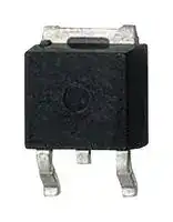
Power MOSFET, P Channel, 60 V, 7.8 A, 0.28 ohm, TO-252 (DPAK), Surface Mount
- Manufacturer: ONSEMI
- Product type: Single MOSFETs
- Transistor Polarity:P Channel; Continuous Drain Current Id:-7.8A; Drain Source Voltage Vds:-60V; On Resistance Rds(on):0.28ohm; Rds(on) Test Voltage Vgs:-10V; Threshold Voltage Vgs:-4V; Power Dissip
- No. of Pins: 3Pins
- Channel Type: P Channel
- Product Range: -
- Qualification: -
- Power Dissipation: 32W
- Transistor Mounting: Surface Mount
- Rds(on) Test Voltage: 10V
- Transistor Case Style: TO-252 (DPAK)
- Drain Source Voltage Vds: 60V
- Operating Temperature Max: 150°C
- Continuous Drain Current Id: 7.8A
- Drain Source On State Resistance: 0.28ohm
- Gate Source Threshold Voltage Max: 4V
| Delivery and price | |
|---|---|
| Units per pack | 2500 |
| Price | 0.209 € |
| Current stock | 10+ |
| Lead time | 30 days |
## **Advanced  Power  MOSFET**

## **SFR/U9024**

## **FEATURES**

- n Avalanche  Rugged  Technology

- n Rugged  Gate  Oxide  Technology

- n Lower  Input  Capacitance

- n Improved  Gate  Charge

- n Extended  Safe  Operating  Area

- n Lower  Leakage  Current  :  10 µA (Max.)  @  VDS = -60V

- n Lower  RDS(ON) :  0.206 Ω (Typ.)

**==> picture [93 x 145] intentionally omitted <==**

**----- Start of picture text -----**<br>
BVDSS =  -60 V<br>R =  0.28 Ω<br>DS(on)<br>ID =  -7.8 A<br>D-PAK I-PAK<br>2<br>1 1<br>3 23<br>1. Gate  2. Drain  3. Source<br>**----- End of picture text -----**<br>


## **Absolute  Maximum  Ratings**

|**Symbol**|**Characteristic**|**Value**|**Units**|
|---|---|---|---|
|**Symbol**<br>VDSS|Drain-to-Source Voltage|-60|V|
|ID|Continuous  Drain  Current  (TC=25<br>oC)<br>Continuous  Drain  Current  (TC=100<br>oC)|-7.8<br>-5.5|A|
|IDM|Drain  Current-Pulsed<br>O1|31|A|
|VGS|Gate-to-Source  Voltage|±30|V|
|EAS|Single  Pulsed  Avalanche  Energy<br>O<br>2|155|mJ|
|IAR|Avalanche  Current<br>O1|-7.8|A|
|EAR|Repetitive  Avalanche  Energy<br>O1|3.2|mJ|
|dv/dt|Peak  Diode  Recovery dv/dt<br>O<br>3|-5.5|V/ns|
|PD|Total  Power  Dissipation(TA=25<br>oC)<br>*|2.5|W|
||Total  Power  Dissipation  (TC=25<br>oC)<br>Linear Derating Factor|32<br>0.26|W<br>W/<br>oC|
|TJ, TSTG<br>TL|Operating  Junction  and<br>Storage  Temperature  Range<br>Maximum  Lead  Temp.  for  Soldering<br>Purposes,  1/8” from  case  for  5-seconds|- 55  to  +150<br>300|oC|


## **Thermal  Resistance**

|RθJC<br>**Symbol**|Junction-to-Case<br>**Characteristic**|--<br>**Typ.**|3.91<br>**Max.**|oC/W<br>**Units**|
|---|---|---|---|---|
|RθJA|Junction-to-Ambient<br>*|--|50||
|RθJA|Junction-to-Ambient|--|110||


* When  mounted  on  the  minimum  pad  size  recommended (PCB  Mount).

Rev. C

**P-CHANNEL POWER MOSFET**

## **SFR/U9024**

## **Electrical Characteristics** (TC=25[o] C  unless  otherwise  specified)

|**Electri**|**cal Characteristics**(TC=25oC|unle|ss  ot|herwi|se  sp|ecified)|
|---|---|---|---|---|---|---|
|**Symbol**|**Characteristic**|**Min.**|**Typ.**|**Max. **|**Units**|**Test  Condition**|
|BVDSS|Drain-Source  Breakdown  Voltage|-60|--|--|V|VGS=0V,ID=-250µA|
|∆BV/∆TJ|<br>Breakdown  Voltage  Temp. Coeff.|--|-0.04|--|V/<br>oC|ID=-250µA**_See Fig 7_**|
|VGS(th)|Gate  Threshold  Voltage|-2.0|--|-4.0|V|VDS=-5V,ID=-250µA|
|IGSS|Gate-Source  Leakage ,  Forward|--|--|-100|nA|VGS=-20V|
||<br>Gate-Source  Leakage ,  Reverse|--|--|100||VGS=20V|
|IDSS|Drain-to-Source  Leakage  Current|--|--|-10|µA|VDS=-60V|
|||--|--|-100||VDS=-48V,TC=125<br>oC|
|RDS(on)|Static  Drain-Source<br>On-State  Resistance|--|--|0.28|Ω|VGS=-10V,ID=-3.9A<br>O<br>4|
|gfs|Forward  Transconductance|--|3.7|--|S|VDS=-30V,ID=-3.9A<br>O<br>4|
|Ciss<br>Coss|Input  Capacitance<br>Output  Capacitance|--<br>--|140<br>465|600<br>215|pF|VGS=0V,VDS=-25V,f =1MHz<br>**_See Fig 5_**|
|Crss|Reverse  Transfer  Capacitance|--|40|60|||
|td(on)|Turn-On  Delay  Time|--|11|30|ns|VDD=-30V,ID=-9.7A,<br>RG=18<br>**_See Fig 13_**<br>Ω<br>O<br>5<br>O<br>4|
|tr|Rise  Time|--|21|50|||
|td(off)|Turn-Off  Delay  Time|--|29|65|||
|tf|Fall  Time|--|20|50|||
|Qg|Total  Gate  Charge|--|15|19|nC|VDS=-48V,VGS=-10V,<br>ID=-9.7A<br>**_See Fig 6 & Fig 12_**<br>O<br>5<br>O<br>4|
|Qgs|Gate-Source  Charge|--|2.9|--|||
|Qgd|Gate-Drain(“Miller”) Charge|--|6.0|--|||


## **Source-Drain  Diode  Ratings  and  Characteristics**

|**Symbol**|**Characteristic**|**Min.**|**Typ.**|**Max. **|**Units**|**Test  Condition**|
|---|---|---|---|---|---|---|
|IS|Continuous  Source  Current|--|--|-7.8|A|Integral reverse pn-diode<br>in the MOSFET|
|ISM|Pulsed-Source  Current<br>O1|--|--|-31|||
|VSD|Diode  Forward  Voltage<br>O<br>4|--|--|-3.8|V|TJ=25<br>oC,IS=-7.8A,VGS=0V|
|trr|Reverse  Recovery  Time|--|80|--|ns|TJ=25<br>oC,IF=-9.7A<br>diF/dt=100A/µs<br>O<br>4|
|Qrr|Reverse  Recovery  Charge|--|0.22|--|µC||


## **Notes ;**

O[1] Repetitive Rating : Pulse Width Limited by Maximum Junction Temperature O2 L=3.0mH, IAS=-7.8A, VDD=-25V, RG=27Ω*, Starting TJ =25[o] C O3 ISD      _< -9.7A, di/dt _< 250A/µs, VDD _< BVDSS , Starting TJ =25[o] C O4 Pulse Test : Pulse Width = 250µs, Duty Cycle    2%_< O5 Essentially Independent of Operating Temperature

**SFR/U9024**

## **P-CHANNEL POWER MOSFET**

**Fig 1.  Output Characteristics**

**==> picture [196 x 147] intentionally omitted <==**

**----- Start of picture text -----**<br>
                     VGS<br>Top  :          - 15 V<br>                   - 10 V<br>                  - 8.0 V<br>10 [1]                   - 7.0 V<br>                  - 6.0 V<br>                  - 5.5 V<br>                  - 5.0 V<br>Bottom  :   -  4.5 V<br>10 [0]<br>@ Notes :<br>  1. 250  µ s Pulse Test<br>  2. TC = 25 oC<br>10 [-1]<br>10 [-1] 10 [0] 10 [1]<br>-VDS , Drain-Source Voltage  [V]<br> , Drain Current  [A]-ID<br>**----- End of picture text -----**<br>


**Fig 2.  Transfer Characteristics**

**==> picture [202 x 147] intentionally omitted <==**

**----- Start of picture text -----**<br>
10 [1]<br>150 oC<br>10 [0]<br>25 oC @ Notes :<br>  1. VGS = 0 V<br>  2. VDS = -30 V<br>- 55 oC   3. 250  µ s Pulse Test<br>10 [-1]<br>2 4 6 8 10<br>-VGS , Gate-Source Voltage  [V]<br> , Drain Current  [A]-ID<br>**----- End of picture text -----**<br>


**Fig 3.  On-Resistance vs. Drain Current**

**Fig 4.  Source-Drain Diode Forward Voltage**

**==> picture [431 x 340] intentionally omitted <==**

**----- Start of picture text -----**<br>
0.40<br>0.35<br>10 [[1]]<br>0.30<br>VGS = -10 V<br>0.25<br>10 [[0]]<br>0.20<br>150 oCoCC<br>@ Notes :<br>0.15 VGS = -20 V @ Note : TJ = 25  [o] C 25 oCoCC   1. V  2. 250 GS = 0 V  2. 250 GS = 0 V µ s Pulse Test<br>0.10 10 [[-1]]<br>0 5 10 15 20 25 30 35 40 0.5 1.0 1.5 2.0 2.5 3.0 3.5<br>-ID , Drain Current  [A] -VSD , Source-Drain Voltage  [V]SD , Source-Drain Voltage  [V] , Source-Drain Voltage  [V]<br>Fig 5.  Capacitance vs. Drain-Source Voltage Fig 6.  Gate Charge vs. Gate-Source Voltage<br>800<br>Ciss= Cgs+ Cgd ( Cds= shorted )<br>Coss= Cds+ Cgd 10 VDS = -12 V<br>600 C iss Crss= Cgd VDSV = -48 VDS = -30 V<br>C oss<br>400<br>@ Notes : 5<br>  1. VGS = 0 V<br>  2. f = 1 MHz<br>200 C rss<br>@ Notes : ID =-9.7 A<br>0 0<br>10 [0] 10 [1] 0 4 8 12 16<br>-VDS , Drain-Source Voltage [V] QG , Total Gate Charge  [nC]<br>]<br>Ω<br> , [<br>DS(on)<br>R<br>Drain-Source On-Resistance<br> , Reverse Drain Current  [A]<br>DR<br>-I<br>Capacitance  [pF]<br> , Gate-Source Voltage  [V]<br>GS<br>-V<br>**----- End of picture text -----**<br>


**==> picture [203 x 141] intentionally omitted <==**

**----- Start of picture text -----**<br>
10 [[1]]<br>10 [[0]]<br>150 oCoCC<br>@ Notes :<br>GS = 0 V = 0 V<br>25 oCoCC   1. V  2. 250 GS = 0 V  2. 250 GS = 0 V µ s Pulse Test<br>10 [[-1]]<br>0.5 1.0 1.5 2.0 2.5 3.0 3.5<br>-VSD , Source-Drain Voltage  [V]SD , Source-Drain Voltage  [V] , Source-Drain Voltage  [V]<br> , Reverse Drain Current  [A]<br>DR<br>-I<br>**----- End of picture text -----**<br>


**P-CHANNEL POWER MOSFET**

## **SFR/U9024**

**Fig 8.  On-Resistance vs. Temperature**

**==> picture [432 x 160] intentionally omitted <==**

**----- Start of picture text -----**<br>
Fig 7.  Breakdown Voltage vs. Temperature Fig 8.  On-Resistance vs. Temperature<br>1.2 2.5<br>2.0<br>1.1<br>1.5<br>1.0<br>1.0<br>0.9 @ Notes : @ Notes :<br>  1. V  2. IGSD = -250  = 0 V µ A 0.5   1. V  2. IGSD = -4.9 A = -10 V<br>0.8 0.0<br>-75 -50 -25 0 25 50 75 100 125 150 175 -75 -50 -25 0 25 50 75 100 125 150 175 200<br>TJ , Junction Temperature  [ [o] C] TJ , Junction Temperature  [ [o] C]<br> , (Normalized)  , (Normalized)<br>-BVDSS RDS(on)<br>Drain-Source On-Resistance<br>Drain-Source Breakdown Voltage<br>**----- End of picture text -----**<br>


**Fig 9.  Max. Safe Operating Area**

**Fig 10.  Max. Drain Current vs. Case Temperature**

**==> picture [425 x 335] intentionally omitted <==**

**----- Start of picture text -----**<br>
8<br>Operation in This Area<br>10 [2] is Limited by R DS(on)<br>6<br>0.1 ms<br>10 [1] 1 ms<br>4<br>10 ms<br>DC<br>@ Notes :<br>10 [0]   1. TC = 25  [o] C<br>  2. TJ = 150  [o] C 2<br>  3. Single Pulse<br>10 [-1] 0<br>10 [0] 10 [1] 10 [2] 25 50 75 100 125 150<br>-VDS , Drain-Source Voltage  [V] Tc , Case Temperature  [ [o] C]<br>Fig 11.  Thermal Response<br>D=0.5<br>@ Notes :<br>10 [0] 0.2   1. Z θ JC (t)=3.91 o C/W Max.<br>  2. Duty Factor, D=t1 /t2<br>0.1   3. TJM -TC =PDM *Z θ JC (t)<br>0.05 P.DM<br>0.02<br>10 [-1] 0.01 t1.t2.<br>single pulse<br>10 [-5] 10 [-4] 10 [-3] 10 [-2] 10 [-1] 10 [0] 10 [1]<br>t1 , Square Wave Pulse Duration  [sec]<br> , Drain Current  [A]-ID<br> , Drain Current  [A]-ID<br>(t) ,  Thermal Response<br>Z JC θ<br>**----- End of picture text -----**<br>


**SFR/U9024**

## **P-CHANNEL POWER MOSFET**

**Fig 12.  Gate Charge Test Circuit  &  Waveform**

**==> picture [385 x 177] intentionally omitted <==**

**----- Start of picture text -----**<br>
“ Current Regulator ”<br>Same Type VGS<br>50K Ω as DUT<br>Qg<br>12V 200nF<br>300nF -10V<br>VDS<br>VGS Qgs Qgd<br>DUT<br>-3mA<br>R1 R2<br>Charge<br>Current Sampling (IG) Current Sampling (ID)<br>Resistor Resistor<br>**----- End of picture text -----**<br>


**Fig 13.  Resistive Switching Test Circuit  &  Waveforms**

**==> picture [439 x 290] intentionally omitted <==**

**----- Start of picture text -----**<br>
RL<br>Vout td(on) t on tr td(off) t off tf<br>Vin VDD<br>( 0.5 rated VDS ) Vin<br>RG 10%<br>DUT<br>-10V<br>90%<br>Vout<br>Fig 14.  Unclamped Inductive Switching Test Circuit  &  Waveforms<br>VDS LL EAS = ----12 LL IAS2 --------------------BVBVDSS -- VDSS DD<br>Vary tp to obtain ID t p Time<br>required peak ID<br>VDD VDS (t)<br>RG C VDD ID (t)<br>DUT<br>-10V IAS<br>t p BVDSS<br>**----- End of picture text -----**<br>


**P-CHANNEL POWER MOSFET**

## **SFR/U9024**

## **Fig 15.  Peak Diode Recovery dv/dt Test Circuit  &  Waveforms**

**==> picture [310 x 465] intentionally omitted <==**

**----- Start of picture text -----**<br>
+<br>VDS<br>DUT<br>--<br>I S<br>L<br>Driver<br>VGS<br>RG Compliment of DUT(N-Channel) VDD<br>VGS • dv/dt controlled by “RG”<br>• IS controlled by Duty Factor “D”<br>Gate Pulse Width<br>VGS D = --------------------------Gate Pulse Period 10V<br>( Driver )<br>Body Diode Reverse Current<br>I S IRM<br>( DUT )<br>di/dt<br>IFM , Body Diode Forward Current<br>Vf<br>VDS<br>( DUT )<br>Body Diode VDD<br>Forward Voltage Drop<br>Body Diode Recovery dv/dt<br>**----- End of picture text -----**<br>


**==> picture [64 x 7] intentionally omitted <==**

**----- Start of picture text -----**<br>
TRADEMARKS<br>**----- End of picture text -----**<br>


**==> picture [439 x 623] intentionally omitted <==**

**----- Start of picture text -----**<br>
The following are registered and unregistered trademarks Fairchild Semiconductor owns or is authorized to use and is<br>not intended to be an exhaustive list of all such trademarks.<br>ACEx™ FACT™ ImpliedDisconnect™ PACMAN™ SPM™<br>ActiveArray™ FACT Quiet Series™ ISOPLANAR™ POP™ Stealth™<br>Bottomless™ FAST® LittlkeFET™ Power247™ SuperSOT™-3<br>CoolFET™ FASTr™ MicroFET™ PowerTrench® SuperSOT™-6<br>CROSSVOLT™ FRFET™ MicroPak™ QFET™ SuperSOT ™-8<br>DOME™ GlobalOptoisolator™ MICROWIRE™ qas™ SyncFET™<br>EcoSPARK™ GTOo™ MSX™ QT Optoelectronics™ TinyLogic™<br>E?CMOS™ HiSeC™ MSXPro™ Quiet Series™ TruTranslation™<br>EnSigna™ 2co™ OCX™ RapidConfigure™ UHC™<br>Across the board. Around the world.™ OCXPro™ RapidConnect™ UltraFET®<br>The Power Franchise™ OPTOLOGIC® SILENT SWITCHER® VCX™<br>Programmable Active Droop™ OPTOPLANAR™ SMART START™<br>DISCLAIMER<br>FAIRCHILD SEMICONDUCTOR RESERVES THE RIGHT TO MAKE CHANGES WITHOUT FURTHER<br>NOTICE TOANY PRODUCTS HEREIN TO IMPROVE RELIABILITY, FUNCTION OR DESIGN. FAIRCHILD<br>DOES NOTASSUMEANY LIABILITY ARISING OUT OF THE APPLICATION OR USE OF ANY PRODUCT<br>OR CIRCUIT DESCRIBED HEREIN; NEITHER DOES IT CONVEY ANY LICENSE UNDER ITS PATENT<br>RIGHTS, NOR THE RIGHTS OF OTHERS.<br>LIFE SUPPORT POLICY<br>FAIRCHILD’S PRODUCTS ARE NOT AUTHORIZED FOR USE AS CRITICAL COMPONENTS IN LIFE SUPPORT<br>DEVICES OR SYSTEMS WITHOUT THE EXPRESS WRITTENAPPROVAL OF FAIRCHILD SEMICONDUCTOR CORPORATION.<br>As used herein:<br>1. Life support devices or systems are devices or 2. A critical component is any component of a life<br>systems which, (a) are intended for surgical implant into support device or system whose failure to perform can<br>the body, or (b) support or sustain life, or (c) whose be reasonably expected to cause the failure of the life<br>failure to perform when properly used in accordance support device or system, or to affect its safety or<br>with instructions for use provided in the labeling, can be effectiveness.<br>reasonably expected to result in significant injury to the<br>user.<br>PRODUCT STATUS DEFINITIONS<br>Definition of Terms<br>Advance Information Formative or This datasheet contains the design specifications for<br>In Design product development. Specifications may change in<br>any manner without notice.<br>Preliminary First Production This datasheet contains preliminary data, and<br>supplementary data will be published at a later date.<br>Fairchild Semiconductor reserves the right to make<br>changes at any time without notice in order to improve<br>design.<br>No Identification Needed Full Production This datasheet contains final specifications. Fairchild<br>Semiconductor reserves the right to make changes at<br>any time without notice in order to improve design.<br>Obsolete Not In Production This datasheet contains specifications on a product<br>that has been discontinued by Fairchild semiconductor.<br>The datasheet is printed for reference information only.<br>Rev. I1<br>**----- End of picture text -----**<br>
Updated at March 10, 2026
onsemi is a premier global supplier of intelligent power and sensing technologies, driving disruptive innovations across the automotive, industrial, and cloud infrastructure markets. Recognized for their commitment to sustainability and reliable supply chains, the company accelerates advancements in vehicle electrification, industrial automation, and 5G networks by solving the industry's most complex design challenges. At the core of their portfolio is an industry-leading selection of discrete semiconductors. This extensive range features thousands of high-performance bipolar transistors, single and dual MOSFETs, and a comprehensive array of diodes, including Zener, Schottky, and fast-recovery rectifiers. Engineered for superior thermal performance and energy efficiency, these foundational components are critical for demanding power conversion, switching, and signal conditioning applications. Beyond essential discretes, onsemi provides a robust suite of advanced power management and circuit protection solutions. Their lineup includes intelligent power modules, single IGBTs, and transient voltage suppression (TVS) diodes designed to safeguard sensitive circuitry. Complimented by integrated passive filters, AC/DC LED driver ICs, and specialized sub-2.4GHz RF transceivers, onsemi equips engineers with the scalable, high-quality technologies needed to build a cleaner, smarter, and more connected world.
About Novapart
Novapart is a B2B electronic component broker specialising in stock shortages and cost reduction. We source hard-to-find parts and identify compliant alternatives across a catalogue of 410,000+ components from 500+ manufacturers.
Learn more →Stock Shortage Specialist
When a component is unavailable, discontinued or has an unacceptable lead time, we tap into our network of vetted European and Asian distributors to source what you need — without compromising on quality or traceability.
Request a quote →Compliant Alternatives
We identify pin-to-pin, electrically equivalent substitutes that meet the same certifications (RoHS, AEC-Q100, REACH) as your original specification — validated against datasheets, not just part numbers. Often at a lower cost.
BOM Analysis service →