


SFH9154
Power MOSFET, P Channel, 150 V, 18 A, 0.2 ohm, TO-3P, Through Hole
- Manufacturer: ONSEMI
- Product type: Single MOSFETs
- Transistor Polarity:P Channel; Continuous Drain Current Id:-18A; Drain Source Voltage Vds:-150V; On Resistance Rds(on):0.2ohm; Rds(on) Test Voltage Vgs:-10V; Threshold Voltage Vgs:-4V; Power Dissipa
- No. of Pins: 3Pins
- Channel Type: P Channel
- Product Range: -
- Qualification: -
- Power Dissipation: 204W
- Transistor Mounting: Through Hole
- Rds(on) Test Voltage: 10V
- Transistor Case Style: TO-3P
- Drain Source Voltage Vds: 150V
- Operating Temperature Max: 150°C
- Continuous Drain Current Id: 18A
- Drain Source On State Resistance: 0.2ohm
- Gate Source Threshold Voltage Max: 4V
| Delivery and price | |
|---|---|
| Units per pack | 450 |
| Price | 0.87 € |
| Current stock | 10+ |
| Lead time | 30 days |
**SFH9154**
## **Advanced Power MOSFET**
## **FEATURES**
- I Avalanche Rugged Technology I Rugged Gate Oxide Technology I Lower Input Capacitance I Improved Gate Charge I Extended Safe Operating Area I 150oC Operating Temperature I Lower Leakage Current : 10 µA (Max.) @ VDS = -150V I Lower RDS(ON) : 0.140 Ω (Typ.)
|BVDSS = -150 V|
|---|
|RDS(on)= 0.2Ω|
|ID = -18 A|
||
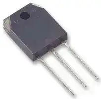
|**TO-3P**|
|**2**<br>**1**|
|**3**|
|**1.Gate 2. Drain 3. Source**|
## **Absolute Maximum Ratings**
|**Symbol**<br>a|**Characteristic**|**Value**|**Units**|
|---|---|---|---|
|VDSS<br>a|Drain-to-Source Voltage<br>|-150|V|
|ID<br> <br>a|Continuous Drain Current (TC=25<br>oC)<br> pT|-18|A|
||Continuous Drain Current (TC=100<br>oC)<br>pO|-11.5||
|IDM<br>a|Drain Current-Pulsed①<br>pO|-72|A|
|VGS<br>a<br>a|Gate-to-Source Voltage<br>pO|±30|V|
|EAS<br>a|Single Pulsed Avalanche Energy②|1215|mJ|
|IAR<br>a|Avalanche Current①|-18|A|
|EAR<br>a|Repetitive Avalanche Energy①<br> ee|20.4<br>ee|mJ<br>ee|
|dv/dt|Peak Diode Recovery dv/dt<br>③|-5.0|V/ns|
|PD|Total Power Dissipation (TC=25<br>oC)<br>Linear Derating Factor|204<br>1.63|W<br>W/<br>oC|
|TJ, TSTG<br>TL|Operating Junction and<br>Storage Temperature Range<br>Maximum Lead Temp. for Soldering<br>Purposes, 1/8"from case for 5-seconds|- 55 to +150<br>300|oC|
## **Thermal Resistance**
|RθJC<br>**Symbol**|Junction-to-Case<br>**Characteristic**|--<br>**Typ.**|0.61<br>**Max.**|oC/W<br>**Units**|
|---|---|---|---|---|
|RθCS|Case-to-Sink|0.24|--||
|RθJA|Junction-to-Ambient|--|40||
1
**P-CHANNEL POWER MOSFET**
**SFH9154**
**Electrical Characteristics** (TC=25℃ unless otherwise specified)
|**Symbol**<br>aDR|**Characteristic**<br>DR|**Min.**<br>ee|**Typ.**<br>ee|**Max. **|**Units**|**Test Condition**|
|---|---|---|---|---|---|---|
|BVDSS<br>aDR<br>OO<br>a|Drain-Source Breakdown Voltage<br>DR<br>OO<br>ee|-150<br>ee<br>OO<br>ee|--<br>ee<br>OO<br>ee|--<br>OO|V<br>OO|VGS=0V,ID=-250μA<br>OO|
|ΔBV/ΔTJ<br>a|Drain-Source Breakdown Voltage<br>Breakdown Voltage Temp. Coeff.<br>ee|--<br>ee|-0.16<br>ee|--|V/℃|ID=-250μA**_See Fig 7_**|
|VGS(th)<br>a<br>a|Gate Threshold Voltage<br>ee <br>sO|-2.0<br> ee <br>sO<br>ee|--<br> ee<br>sO<br>ee|-4.0<br>sO<br>e|V<br>sO<br>ee|VDS=-5V,ID=-250μA<br>sO|
|IGSS<br>e<br>p|Gate-Source Leakage , Forward<br>ee<br>po|--<br>e<br>ee<br>o|--<br>e<br>ee<br>o|-100<br>e<br>e|nA<br>ee<br>ee<br>Pp<br>~~ee~~|VGS=-30V<br>e<br>Pp|
||Gate-Source Leakage , Forward<br>Gate-Source Leakage , Reverse<br>ee<br>po|--<br>e<br>ee<br>o<br>~~ee~~|--<br>e<br>ee<br>o<br>~~ee~~|100<br>e<br>e<br>~~ee~~||VGS=30V<br>e<br>Pp<br>eee|
|IDSS<br>p<br>~~ee~~|Drain-to-Source Leakage Current<br>po<br>~~ee~~|--<br>ee<br>o<br>~~ee~~<br>~~ee~~|--<br>ee <br>o<br>~~ee~~<br>~~ee~~|-10<br> e<br>~~ee~~<br>~~ee~~|μA<br>ee<br>Pp<br>~~ee~~<br>~~ee~~|VDS=-150V<br>Pp<br>~~ee~~<br>eee|
|||--<br>~~ee~~<br>~~ee~~|--<br>~~ee~~<br>~~ee~~|-100<br>~~ee~~<br>~~ee~~||VDS=-120V,TC=125℃<br>~~ee~~<br>eee|
|RDS(on)|Static Drain-Source<br>On-State Resistance|--<br>~~ee~~|0.14 0.2<br>~~ee~~|0.14 0.2<br>~~ee~~|Ω<br>~~ee~~|VGS=-10V,ID=-9.0A④<br> eee|
|gfs<br>a<br>a|Forward Transconductance<br>|--<br>eeee<br>|11<br>ee<br>|--<br>ee<br>|Ω|VDS=-40V,ID=-9.0A<br>④|
|Ciss<br>Coss<br>aee<br>aee<br>a|Input Capacitance<br>Output Capacitance<br>ee<br>ee<br>|--<br>--<br>ee<br>eeee<br>ee<br>eeeee<br>|400<br>2290<br>ee<br>ee<br>ee<br>eee<br>|3000<br>600<br>ee<br>ee<br>ee<br>eee<br>|pF<br>eee|VGS=0V,VDS=-25V,f =1MHz<br>**_See Fig 5_**|
|Crss<br>aDe|Reverse Transfer Capacitance<br>De|--<br>eeeee<br>De|200<br>eee<br>De|300<br>eee<br>De|||
|td(on)<br>a|Turn-On Delay Time|--|20|45|ns|VDD=-75V,ID=-18A,<br>RG=6.2Ω<br>**_See Fig 13_**④⑤|
|tr<br>aDe|Rise Time<br>De|--<br>De|40<br>De|90<br>De|||
|td(off)<br>aDe|Turn-Off Delay Time<br>De|--<br>De|80<br>De|170<br>De|||
|tf<br>De<br>a|Fall Time<br>De|--<br>De<br>ee|40<br>De|90<br>De|||
|Qg<br>a<br>a|Total Gate Charge<br>ee|--<br>ee<br>ee|100<br>ee|130|nC|VDS=-120V,VGS=-10V,<br>ID=-18A<br>**_See Fig 6 & Fig 12_**④⑤|
|Qgs<br>a|Gate-Source Charge|--<br>ee|20|--|||
|Qgd<br>~~a~~|Gate-Drain("Miller") Charge|--|40|--|||
## **Source-Drain Diode Ratings and Characteristics**
|**Symbol**|**Characteristic**|**Min.**|**Typ.**|**Max. **|**Units**|**Test Condition**|
|---|---|---|---|---|---|---|
|IS|Continuous Source Current|--|--|-18|A|Integral reverse pn-diode<br>in the MOSFET|
|ISM|Pulsed-Source Current①|--|--|-72|||
|VSD|Diode Forward Voltage④|--|--|-5.0|V|TJ=25℃,IS=-18A,VGS=0V|
|trr|Reverse Recovery Time|--|200|--|ns|TJ=25℃,IF=-18A<br>diF/dt=100A/μs④|
|Qrr|Reverse Recovery Charge|--|1.5|--|μC||
## **Notes ;**
- ① Repetitive Rating : Pulse Width Limited by Maximum Junction Temperature
- ② L=5mH, IAS=-18A, VDD=-50V, RG=27Ω, Starting TJ =25℃
- ③ ISD≤-18A, di/dt≤450A/μs, VDD≤BVDSS , Starting TJ =25℃
- ④ Pulse Test : Pulse Width = 250μs, Duty Cycle ≤ 2%
- ⑤ Essentially Independent of Operating Temperature
2
**P-CHANNEL POWER MOSFET**
**SFH9154**
**==> picture [113 x 9] intentionally omitted <==**
**----- Start of picture text -----**<br>
Fig 1. Output Characteristics<br>**----- End of picture text -----**<br>
**==> picture [119 x 9] intentionally omitted <==**
**----- Start of picture text -----**<br>
Fig 2. Transfer Characteristics<br>**----- End of picture text -----**<br>
**==> picture [428 x 518] intentionally omitted <==**
**----- Start of picture text -----**<br>
-VGS 10 [2]<br>Top : 15 V @ Notes :<br>10 [2] 10 V 8.0 V 7.0 V 1. 250 2. TC = 25 µ s Pulse TestoC ——<br> 6.0 V<br> 5.5 V<br> 5.0 V 10 [1]<br>Bottom : 4.5 V<br>10 [1]<br>150 oC @ Notes :<br>10 [0] 1. VGS = 0 V<br>25 oC 2. VDS = 40 V<br> 3. 250 µ s Pulse Test<br>- 55 oC<br>10 [0] 10 [-1]<br>10 [-1] Pam 10 [0] 10 [1] 0 y 2 4 e 6 8 10<br>-VDS , Drain-Source Voltage [V] -VGS , Gate-Source Voltage [V]<br>Fig 3. On-Resistance vs. Drain Current Fig 4. Source-Drain Diode Forward Voltage<br>0.24<br>10 [2]<br>0.20<br>VGS = -10 V 10 [1]<br>0.16<br>| ee<br>VGS = -20 V<br>10 [0]<br>0.12 @ Notes :<br>A | | 150 oC 1. VGS = 0 V<br>@ Note : TJ = 25 [o] C 25 oC 2. 250 µ s Pulse Test<br>0.08 10 [-1]<br>0 15 30 45 60 75 90 0.5 1.0 1.5 2.0 2.5 3.0 3.5 4.0 4.5<br>-ID , Drain Current [A] -VSD , Source-Drain Voltage [V]<br>Fig 5. Capacitance vs. Drain-Source Voltage Fig 6. Gate Charge vs. Gate-Source Voltage<br>5000 15<br>Ciss= Cgs+ Cgd ( Cds= shorted )<br>Coss= Cds+ Cgd<br>4000 C iss Crss= Cgd VDS = -30 V<br>10 VDS = -75 V<br>3000 VDS = -120 V<br>C oss fe e S<br>2000<br>C rss @ Notes : 5<br> 1. VGS = 0 V<br>1000 2. f = 1 MHz<br>@ Notes : ID = -18 A<br>0 0<br>10 [0] 10 [1] 0 20 40 60 80 100<br>-VDS , Drain-Source Voltage [V] QG , Total Gate Charge [nC]<br> , Drain Current [A]-ID , Drain Current [A]-ID<br>]<br> Ω<br> , [<br>DS(on)<br>R<br> , Reverse Drain Current [A]<br>DR<br>Drain-Source On-Resistance<br>-I<br>Capacitance [pF]<br> , Gate-Source Voltage [V]<br>GS<br>-V<br>**----- End of picture text -----**<br>
3
**P-CHANNEL POWER MOSFET**
**SFH9154**
**==> picture [438 x 531] intentionally omitted <==**
**----- Start of picture text -----**<br>
Fig 7. Breakdown Voltage vs. Temperature Fig 8. On-Resistance vs. Temperature<br>1.2 2.0<br>1.1 1.6<br>1.0<br>1.2<br>0.9 @ Notes : @ Notes :<br> 1. VGS = 0 V 0.8 1. Vgs = -10V<br> 2. ID = 250 µ A 2. Id = -9A<br>0.8<br>-75 -50 -25 0 25 50 75 100 125 150 175 -75 -50 -25 0 25 50 75 100 125 150 175<br>TJ , Junction Temperature [ [o] C] TJ , Junction Temperature [ [o] C]<br>Fig 9. Max. Safe Operating Area Fig 10. Max. Drain Current vs. Case Temperature<br>10 [3] 20<br>Operation in This Area<br>is Limited by R DS(on)<br>10 [2] 15<br>0.1 ms<br>1 ms<br>10 ms<br>10 [1] DC 10<br>@ Notes :<br> 1. TC = 25 [o] C<br>10 [0] 2. TJ = 150 [o] C 5<br> 3. Single Pulse<br>10 [-1] 0<br>10 [0] 10 [1] 10 [2] 25 50 75 100 125 150<br>Fa m e Pa<br>-VDS , Drain-Source Voltage [V] Tc , Case Temperature [ [o] C]<br>Fig 11. Thermal Response<br>10 [0]<br>e D=0.5 ee<br>ae<br>0.2<br>@ Notes :<br>10 [-1] Se 0.1 1. Z θ JC(t) = 0.61 oC/W Max.<br>0.05 2. Duty Factor, D = t1/t2<br>0.02 3. TJM-TC = PDM*Z θ JC(t)<br>10 [-2] Z 0.01 F single pulse = wa PDM t1 fr a<br>t2<br>10 20 [-5] 10 [-4] eee 10 [-3] 10 [-2] eee 10 [-1] 10 [0] 10 [1]<br>t1 , Square Wave Pulse Duration [sec]<br> , (Normalized)<br> , (Normalized)<br>DSS<br>DS(on)<br>R<br>-BV<br>Drain-Source Breakdown Voltage Drain-Source On-Resistance<br> , Drain Current [A]-ID , Drain Current [A]D<br>-I<br>(t) , Thermal Response<br>ZJC θ<br>**----- End of picture text -----**<br>
4
**P-CHANNEL POWER MOSFET**
**SFH9154**
**Fig 12. Gate Charge Test Circuit & Waveform**
**==> picture [439 x 515] intentionally omitted <==**
**----- Start of picture text -----**<br>
* Current Regulator ”<br>Same Type VGS<br>50K Ω as DUT<br>Qg<br>12V 200nF<br>300nF -10V<br>VDS<br>VGS Qgs Qgd<br>DUT<br>-3mA<br>+ —> R1 R2 (<br>a<br>Charge<br>Current Sampling (IG) Current Sampling (ID)<br>Resistor Resistor<br>Fig 13. Resistive Switching Test Circuit & Waveforms<br>RL<br>Vout a td(on) t on tr AS td(off) t off tf<br>Vin VDD<br>( 0.5 rated VDS ) Vin<br>RG 10%<br>DUT<br>-10V<br>90%<br>_ Vout<br>Fig 14. Unclamped Inductive Switching Test Circuit & Waveforms<br>VDS LL EAS = ----12 LL IAS2 --------------------BVBVDSS -- VDSS DD<br>Vary tp to obtain ID t p Time<br>required peak ID<br>VDD VDS (t)<br>RG C VDD ID (t)<br>DUT<br>-10V IAS<br>t p BVDSS<br>**----- End of picture text -----**<br>
5
**P-CHANNEL POWER MOSFET**
**SFH9154**
**Fig 15. Peak Diode Recovery dv/dt Test Circuit & Waveforms**
**==> picture [309 x 450] intentionally omitted <==**
**----- Start of picture text -----**<br>
+<br>VDS<br>DUT<br>--<br>I S<br>L<br>Driver<br>VGS<br>RG Compliment of DUT(N-Channel) VDD<br>VGS • dv/dt controlled by 밨 G<br>• IS controlled by Duty Factor “D”<br>Gate Pulse Width<br>VGS D = --------------------------Gate Pulse Period 10V<br>( Driver )<br>a es<br>Body Diode Reverse Current<br>I S IRM<br>( DUT )<br>di/dt<br>SK<br>IFM , Body Diode Forward Current<br>Vf<br>VDS<br>( DUT )<br>Body Diode VDD<br>Forward Voltage Drop<br>Body Diode Recovery dv/dt<br>**----- End of picture text -----**<br>
6
Updated at March 10, 2026
onsemi is a premier global supplier of intelligent power and sensing technologies, driving disruptive innovations across the automotive, industrial, and cloud infrastructure markets. Recognized for their commitment to sustainability and reliable supply chains, the company accelerates advancements in vehicle electrification, industrial automation, and 5G networks by solving the industry's most complex design challenges. At the core of their portfolio is an industry-leading selection of discrete semiconductors. This extensive range features thousands of high-performance bipolar transistors, single and dual MOSFETs, and a comprehensive array of diodes, including Zener, Schottky, and fast-recovery rectifiers. Engineered for superior thermal performance and energy efficiency, these foundational components are critical for demanding power conversion, switching, and signal conditioning applications. Beyond essential discretes, onsemi provides a robust suite of advanced power management and circuit protection solutions. Their lineup includes intelligent power modules, single IGBTs, and transient voltage suppression (TVS) diodes designed to safeguard sensitive circuitry. Complimented by integrated passive filters, AC/DC LED driver ICs, and specialized sub-2.4GHz RF transceivers, onsemi equips engineers with the scalable, high-quality technologies needed to build a cleaner, smarter, and more connected world.
About Novapart
Novapart is a B2B electronic component broker specialising in stock shortages and cost reduction. We source hard-to-find parts and identify compliant alternatives across a catalogue of 410,000+ components from 500+ manufacturers.
Learn more →Stock Shortage Specialist
When a component is unavailable, discontinued or has an unacceptable lead time, we tap into our network of vetted European and Asian distributors to source what you need — without compromising on quality or traceability.
Request a quote →Compliant Alternatives
We identify pin-to-pin, electrically equivalent substitutes that meet the same certifications (RoHS, AEC-Q100, REACH) as your original specification — validated against datasheets, not just part numbers. Often at a lower cost.
BOM Analysis service →