
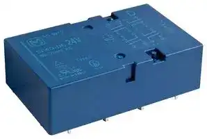


SF4D-DC5V
Safety Relay, 5 VDC, 4PST-NO, 4PST-NC, SF Series, Through Hole, 6 A, Solder
- Manufacturer: PANASONIC
- Product type: Safety Relays
- Coil Voltage:5VDC; Contact Configuration:4PST-NO, 4PST-NC; Product Range:SF Series; Relay Mounting:Through Hole; Contact Current:6A; Relay Terminals:Solder; Contact Voltage AC No
- SVHC: No SVHC (23-Jan-2024)
- IP Rating: -
- Coil Voltage: 5VDC
- Product Range: SF Series
- Relay Mounting: Through Hole
- Contact Current: 6A
- Relay Terminals: Solder
- Contact Material: Silver Tin Oxide
- Approvals & Standards: CSA, UL
- Contact Configuration: 4PST-NO, 4PST-NC
- Contact Voltage AC Nom: 250V
- Contact Voltage DC Nom: 30V
| Delivery and price | |
|---|---|
| Units per pack | 20 |
| Price | 26.55 € |
| Current stock | 200+ |
| Lead time | 30 days |
## **Flat type safety relays (double contact)**

## SF RELAYS Double contact type

## **FEATURES**

2 Form A 2 Form B

4 Form A 4 Form B

## **RoHS compliant** [

## **1. High contact reliability**

High contact reliability is achieved through the use of a double contact.

## **2. Forced operation contacts**

N.O. and N.C. side contacts are connected through a card so that one interacts with the other in movement. In case of a contact welding, the other keeps a min. 0.5mm .020inch contact gap.

## **3. Independent operation contacts (4 Form A  4 Form B)**

There are 4 points of forced operation contacts.

Each pair of contacts is free from the main armature and is independent from each other. So if a N.O. pair of contacts are welded, the other 3 N.O. contacts are not effected (operate properly) That enables to plan a circuit to detect welding or go back to the beginning condition.

## **4. Separated chamber structure**

N.O. and N.C. side contacts are put in each own space surrounded with a card and a body-separater. That prevents short circuit between contacts, which is caused by their springs welding or damaged.

## **5. High breakdown voltage**

High breakdown voltage 2,500 Vrms between contacts and coil.

## **6. High sensitivity**

Realizes thin shape and high sensitivity (500 mW nominal operating power) by utilizing high-efficiency polarized magnetic circuit with 4-gap balanced armature.

**7. Complies with safety standards** Standard products are UL, CSA, TÜV and SEV certified. Conform to European standards. TÜV certified. Complies with SUVA European standard.

## **TYPICAL APPLICATIONS**

**1. Industrial equipment such as presses and machine tools 2. Elevators and other kinds of hoisting mechanisms, conveyor equipment.**

## **ORDERING INFORMATION**

**SF D** Contact arrangement 2: 2 Form A 2 Form B 4: 4 Form A 4 Form B Nominal coil voltage DC 5, 12, 24, 48, 60V —___T J Note: Certified by UL, CSA, TÜV and SEV

## **TYPES**

> Contact arrangement ~~|tC~~ Nominal coil voltage Part No. ~~|~~ 5V DC SF2D-DC5V ~~Po~~ 12V DC SF2D-DC12V

> 2 Form A 2 Form B ~~|~~ —“‘CsisSCisCS 24V DC SF2D-DC24V ~~|~~ t—“;‘S:sSCsisCS 48V DC SF2D-DC48V 60V DC SF2D-DC60V ~~| Pe~~ 5V DC SF4D-DC5V ~~|~~ —“‘CsisSCisCS 12V DC SF4D-DC12V

> 4 Form A 4 Form B ~~|~~ t—“;‘S:sSCsisCS 24V DC SF4D-DC24V 48V DC SF4D-DC48V ~~| PO~~ 60V DC SF4D-DC60V

Standard packing: Carton: 20 pcs.; Case: 200 pcs.

ASCTB120E  201408-T

–1–

SF Double contact type

## **RATING**

## **1. Coil data**

|**RATING**<br>**1. Coil data**|**RATING**<br>**1. Coil data**|||||||||||
|---|---|---|---|---|---|---|---|---|---|---|---|
|Contact<br>arrangement||Nominal coil<br>voltage|Pick-up voltage<br>(at 20°C68°F)||Drop-out voltage<br>(at 20°C68°F)||Nominal coil current<br>[±10%]<br>(at 20°C68°F)|Coil resistance<br>[±10%]<br>(at 20°C68°F)||Nominal operating<br>power<br>(at 20°C68°F)|Max. applied<br>voltage<br>(at 20°C68°F)|
|2 Form A 2 Form B||5V DC|75%V or less of<br>nominal voltage<br>(Initial)||10%V or more of<br>nominal voltage<br>(Initial)||100mA|50Ω||500mW|120%V of<br>nominal voltage|
|||12V DC|||||41.7mA|288Ω||||
|||24V DC|||||20.8mA|1,152Ω||||
|||48V DC|||||10.4mA|4,608Ω||||
|||60V DC|||||8.3mA|7,200Ω||||
|4 Form A 4 Form B||5V DC|75%V or less of<br>nominal voltage<br>(Initial)||15%V or more of<br>nominal voltage<br>(Initial)||100mA|50Ω||500mW||
|||12V DC|||||41.7mA|288Ω||||
|||24V DC|||||20.8mA|1,152Ω||||
|||48V DC|||||10.4mA|4,608Ω||||
|||60V DC|||||8.3mA|7,200Ω||||
|**2. Specifcations**||||||||||||
|Characteristics|Item||||||Specifcations|||||
|Contact|Arrangement|||||2 Form A 2 Form B|||4 Form A 4 Form B|||
||Contact resistance(Initial)|||||Max. 30 mΩ (Byvoltage drop6 V DC 1A)||||||
||Contact material|||||Au-fashed AgSnO2type||||||
|Rating|Nominal switchingcapacity (resistive load)|||||6A 250V AC, 6A 30V DC||||||
||Max. switching power(resistive load)|||||1,500VA 180W||||||
||Max. switchingvoltage|||||440V AC, 30V DC||||||
||Max. switchingcurrent|||||6A||||||
||Nominal operating power|||||500mW||||||
||Min. switchingcapacity (Reference value)*1|||||100mA 5V DC||||||
|Electrical<br>characteristics|Insulation resistance(Initial)|||||Min. 1,000MΩ (at 500V DC)Measurement at same location as “Breakdown voltage” section.||||||
||Breakdown voltage<br>(Initial)|||Between open contacts||1,300 Vrms for 1min.(Detection current: 10mA)||||||
|||||Between contact sets||2,500 Vrms for 1min.(Detection current: 10mA)||||||
|||||Between contact and coil||2,500 Vrms for 1min.(Detection current: 10mA)||||||
||Temperature rise (coil) (at 20° 68°F)|||||Max. 45°C113°F<br>(Byresistive method, nominal voltage applied to the coil; contact carryingcurrent: 6A)||||||
||Operate time|||||Max. 30ms(Nominal voltage applied to the coil, excludingcontact bounce time.)||||||
||Release time|||||Max. 15ms (Nominal voltage applied to the coil, excluding contact bounce time.)<br>(without diode)||||||
|Mechanical<br>characteristics|Shock resistance|||Functional||Min. 294 m/s2 (Half-wavepulse of sine wave: 11 ms; detection time: 10μs)||||||
|||||Destructive||Min. 980 m/s2 (Half-wavepulse of sine wave: 6 ms)||||||
||Vibration resistance|||Functional||10 to 55 Hz at double amplitude of 2 mm(Detection time: 10μs)||||||
|||||Destructive||10 to 55 Hz at double amplitude of 2 mm||||||
|Expected life|Mechanical|||||Min. 107 (at 180 times/min.)||||||
||Electrical|||||Min. 105 (at 20 times/min.)||||||
|Conditions|Conditions for operation, transport and storage*2|||||Ambient temperature: –40°C to +70°C–40°F to +158°F<br>Humidity: 5 to 85% R.H.(Not freezingand condensingat low temperature)||||||
||Max. Operatingspeed|||||180 times/min.||||||
|Unit weight||||||Approx. 38g 1.34oz|||Approx. 47g 1.66oz|||


Notes: *1. This value can change due to the switching frequency, environmental conditions and desired reliability level, therefore it is recommended to check this with the actual load.

*2. The upper limit of the ambient temperature is the maximum temperature that can satisfy the coil temperature rise value. Refer to Usage, transport and storage conditions in NOTES.

ASCTB120E  201408-T

–2–

SF Double contact type

## **REFERENCE DATA**

1. Operate/release time (without diode) Tested sample: SF2D-DC24V (2 Form A 2 Form B) Quantity: n = 20

2. Temperature rise Tested sample: SF4D-DC24V (4 Form A 4 Form B) Quantity: n = 6 Coil applied voltage: 100%V, 120%V Contact carry current: 6A

3. Ambient temperature characteristics Tested sample: SF4D-DC24V (4 Form A 4 Form B) Quantity: n = 6

**==> picture [507 x 133] intentionally omitted <==**

**----- Start of picture text -----**<br>
50 30 100<br>40 P| | fd [i 25 Pt Inside the coil | tt || | 50 Lt<br>20 Drop-out voltage<br>30 BGRaEE Seecan Soh +|<br>-40 -20 0 Pick-up voltage<br>Operate time 15 ett aneoe 20 40 60 80<br>| 2010 SS Release time SSa= MMin.Mxx ax.ax. P= 105 Pitt Contact Ty—| pataPear 4 || -50 Ambienttemperature, °C<br>Min.<br>0 70 ~ 80 90 100 110 — 120 130 0 PEt] 100 rT fT 110 tt 120 rTCEP PT -100 Eee<br>Coil applied voltage, %V Coil applied voltage, %V<br>C° Rate of change, %<br>Temperature rise,<br>Operate/release time, ms<br>**----- End of picture text -----**<br>


## **DIMENSIONS** (mm inch)

> The CAD data of the products with a au=» **CAD Data** mark can be downloaded from: http://industrial.panasonic.com/ac/e/

## **1. 2 Form A 2 Form B**

## External dimensions

**==> picture [293 x 148] intentionally omitted <==**

**----- Start of picture text -----**<br>
GD CAD Data<br>16±0.5<br>.630±.020<br>U p |]<br>0.5<br>.020<br>.0391.0 TT .2005.08 .500 12.7 w .500 12.7 T 12.7 .500 1.0.039 my .1183.0± | 0.5±.020<br>53.3±0.5<br>_ 2.098±.020 ——— 0.48<br>.0120.30 5 6 7 8 .019<br>25.0<br>.984 re| 1 CJ 0  C 1 4 LL<br>7.62 12.7<br>.300 .500<br>Feo a 2 |<br>Oo o a a<br>9 10 11 12<br>**----- End of picture text -----**<br>


General tolerance: ±0.3 ±.012

Schematic (Bottom view) 5 6 7 8 1 ~~‘~~ 2 +3 U8 9 10 11 12 rrara PC board pattern (Bottom view) 10-1.4 dia. holes 2.54 10-.055 dia. holes .100 2.54 .100 ~~SUSE[TTTuEEEUTEEEEEETtT ety ty eye et ty VSDye LATPEREEEEEEEESCSYT TTT [YT TT TETeeeTey ey ey yt yy REE EEE EEE EEL [YT ATT IT TALTTT TATE TAY LP iyt ttt yet ete ty | LTT PTT Ty ere yyy Pte yy LPT ttt tT tity et ye ey yy et~~ LETT TT PEPE Tr ~~[Pretty)]~~ Tolerance: ±0.1 ±.004

**==> picture [502 x 205] intentionally omitted <==**

**----- Start of picture text -----**<br>
2. 4 Form A 4 Form B<br>GD CAD Data External dimensions Schematic (Bottom view)<br>13 14 15 16<br>16±0.5 1<br>.630±.020<br>5 6 7 8<br>a 0.5 e 9 10 e 11 12<br>.020 2<br>.0391.0 Ety 5.08.200 S 12.7 .500 oo? 12.7 .500 12.7 .500 ai e 1.0.039 .1183.0±0.5±.020 a 29 17 18 e 19 ce 20<br>53.3±0.5 0.48<br>x 2.098±.020 —— .019<br>1.29933±±0.5.020 0.30.012 | 1 i 135 146 157 168 .3007.62 PC board pattern (Bottom view)2.54.100 18-.055 dia. holes18-1.4 dia. holes18-1.4 dia. holes<br>7.62 0.48 12.7 2.54<br>.300 .019 .500 .100<br>o 2 = 9 10 11 12 7.62 LPTEERytEEEtttEERytEEEtttytEEEtttEEEtttttt yEEEet eee eee et eee eee<br>17 18 19 20 .300<br>CoC | Pe uRUn EREDSUEUR<br>j—___—_—_J) LTT ty yy ete e yyy eye eye<br>Lotti titi titty ty<br>eT Sree Sree<br>General tolerance: ±0.3 ±.012<br>**----- End of picture text -----**<br>


**==> picture [144 x 106] intentionally omitted <==**

**----- Start of picture text -----**<br>
2.54.100.100 18-.055 dia. holes18-1.4 dia. holes18-1.4 dia. holes<br>2.54<br>.100 LPTEERytEEEtttEERytEEEtttytEEEtttEEEtttttt yEEEet eee eee |<br>Pe uRUn EREDSUEUR<br>LTT ty yy ete e yyy eye eye yyy<br>Lotti titi titty ty tte<br>eT Sree Sree cr<br>EEEEEEEEEEEEEELE<br>COR Cer Fercee<br>LETY  TTT yer Pry tT ter)<br>Tolerance: ±0.1 ±.004<br>**----- End of picture text -----**<br>


ASCTB120E  201408-T

–3–

SF Double contact type

## **SAFETY STANDARDS**

|**SAFETY STANDARDS**|**SAFETY STANDARDS**|||||
|---|---|---|---|---|---|
|UL/C-UL(Recognized)||TÜV(Certifed)||SEV||
|File No.|Contact rating|File No.|Rating|File No.|Contact rating|
|E120782*<br> <br>|6A 250V AC<br>6A 24V DC<br>96<br>96|8 EZ 116.03/10 (SF2D)<br>8 EZ 116.02/09(SF4D)|3A 24V DC<br>6A 250V AC<br>|12.0520|6A 24V DC<br>6A 250V AC|


* CSA standard: Certified by C-UL

## **SAFETY STRUCTURE OF SF RELAYS**

This SF relay design ensures that subsequent operations shut down and can automatically return to a safe state when the SF relay suffers overloading and other circuit abnormalities

(unforeseen externally caused circuit or device breakdowns, end of life incidents, and noise, surge, and environmental influences) owing to contact welding, spring fusion or, in the worst-case

scenario, relay breakdown (coil rupture, faulty operation, faulty return, and fatigue and breakage of the operating spring and return spring), and even in the event of end of life.

||||Structure|Structure|Operation|
|---|---|---|---|---|---|
|1. Forced operation method<br>(2 Form A 2 Form B,<br>4 Form A 4 Form B types)|The two co<br>of each co||||Even when one contact is welded closed, the other<br>maintains a gap of greater than 0.5 mm.020 inch.<br>In the diagram on the left, the lower contact “b” have<br>welded but the upper contact “a” maintain at a gap of<br>greater than 0.5 mm.020 inch.<br>Subsequent contact movement is suspended and the<br>weld can be detected|
|||||||
|2. Independent operation method<br>(4 Form A 4 Form B type)|None of four contacts are held in position by the armature. Even though one<br>of the external N.O. contacts has welded, the other three contacts have<br>returned owingto the de-energizingof the coil.<br>Return<br>Return<br>External NO<br>contact weld<br>Return||||Enables design of safety circuits that allow weld<br>detection and return at an early stage.<br>As shown at the top right of the diagram on the left, if<br>the external N.O. contact welds, a 0.5 mm.020 inch<br>gap is maintained.<br>Each of the other contacts returns to N.O. because<br>the coil is no longer energized.|
|3. Separate chamber method<br>(2 Form A 2 Form B,<br>4 Form A 4 Form B types)|In independent chambers, the contacts “a” a<br>case separator or bythe card itself.<br>Case separator<br>C<br>1|||nd “b” are kept apart by a body/<br>ard<br>Contact a<br>Body<br>separator<br>Contact b<br>2|Prevents shorting and fusing of springs and spring<br>failure owing to short-circuit current.<br>As shown on the diagram on the left, even if the<br>operating springs numbered 1 and 2 there is no<br>shorting between “a” and “b” contacts.|
|4. 2 Form A 2 Form B contact<br>4 Form A 4 Form B contact|Structure with independent COM contact of<br>4 Form A 4 Form B contacts.|||2 Form A 2 Form B and|Independent COM enables differing pole circuit<br>confgurations. This makes it possible to design<br>various kinds of control circuits and safetycircuits.|


ASCTB120E  201408-T

–4–

SF Double contact type

## **THE OPERATION OF SF RELAYS (when contacts are welded)**

**SF relays work to maintain a normal operating state even when the contact welding occur by overloading or short-circuit currents. It is easy to make weld detection circuits and safety circuits in the design to ensure safety even if contacts weld.**

## **1) 2 Form A 2 Form B type**

## Form “b” Contact Weld

If the form “b” contact (No. 1 and 3) welds, the armature becomes non-operational, the contact gaps at the three form “a” contacts are maintained at greater than 0.5 mm .020 inch. Reliable isolation is thus ensured.

**==> picture [507 x 114] intentionally omitted <==**

**----- Start of picture text -----**<br>
No.4 No.1 No.4 No.1<br>Example: If the No. 1 contact welds<br>Each of the three form “a” contacts (No. 2 and 4)<br>maintain a gap of greater than 0.5 mm .020 inch.<br>No.3 No.2 No.3 No.2<br>Non-energized Energized (when No. 1 contact is welded)<br>**----- End of picture text -----**<br>


Form “a” Contact Weld

When the form “a” contacts (No. 2 or 4) weld, the armature remains in a non-returned state and the contact gap at the two form “b” contact is maintained at greater than 0.5 mm .020 inch. Reliable isolation is thus ensured.

**==> picture [526 x 114] intentionally omitted <==**

**----- Start of picture text -----**<br>
No.4 No.1 No.4 No.1<br>Example: If the No. 2 contact welds.<br>The two form “b” contact (No. 1 or 3) maintains a gap of<br>greater than 0.5 mm .020 inch.<br>No.3 No.2 No.3 No.2<br>Energized Non-energized (when No. 2 contact is welded)<br>**----- End of picture text -----**<br>


Contact Operation Table

**==> picture [157 x 114] intentionally omitted <==**

**----- Start of picture text -----**<br>
No.4 No.1<br>No.3 No.2<br>Contact No. No.1 No.2 No.3 No.4<br>Terminal No. 11–12 7–8 5–6 9–10<br>**----- End of picture text -----**<br>


The table below shows the state of the other contacts when the current through the welded form “a” contact is 0 V and the rated voltage is applied through the form “b” contact.

|||State of other contacts|State of other contacts|State of other contacts|State of other contacts||
|---|---|---|---|---|---|---|
|Welded<br>terminal<br>No.|1|<br>1<br>2<br>3<br>4<br>>0.5<br>>0.5||||>0.5: contact gap is kept at<br>min. 0.5 mm.020 inch<br>Empty cells: either closed or open|
||2|>0.5||>0.5|||
||3||>0.5||>0.5||
||4|>0.5||>0.5|||


* Contact gaps are shown at the initial state. If the contacts change state owing to loading/breaking it is necessary to check the actual loading.

ASCTB120E  201408-T

–5–

SF Double contact type

## **2) 4 Form A 4 Form B type**

## Internal Contacts Weld

When internal contacts (No. 2, No. 3, No. 6 or No. 7) are welded, the armature becomes non-operational and the four form “a” contact gaps are maintained at 0.5 mm .020inch or greater. Reliable cut-off is thus ensured.

**==> picture [521 x 114] intentionally omitted <==**

**----- Start of picture text -----**<br>
No.8 No.1 No.8 No.1<br>No.7 No.2 No.7 No.2<br>Example: If the No. 2 contact welds.<br>Each of the four form “a” contacts (No. 1, 3, 5, and 7)<br>No.6 No.3 No.6 No.3 maintains a gap of greater than 0.5 mm .020 inch.<br>No.5 No.4 No.5 No.4<br>Non-energized Energized (when no. 2 contact is welded)<br>**----- End of picture text -----**<br>


## External Contacts Weld

When external contacts (No. 1, No. 4, No. 5 or No. 8) are welded, gaps of 0.5 mm .020inch and greater are maintained between adjacent contacts and other contacts operate normally by the coil being non-energized.

**==> picture [524 x 168] intentionally omitted <==**

**----- Start of picture text -----**<br>
No.8 No.1 No.8 No.1<br>No.7 No.2 No.7 No.2 Example 1: If the No. 1 contact welds.<br>The adjacent No. 2 contact maintains a gap of greater<br>than 0.5 mm .020 inch. The other contacts, because<br>the coil is not energized, return to their normal return<br>No.6 No.3 No.6 No.3 state; each of form “a” contacts (No. 3, 5, and 7)<br>maintains a contact gap of greater than 0.5 mm<br>No.5 No.4 No.5 No.4 .020 inch; each of the form “b” contacts (No. 4, 6, and<br>8) return to a closed state.<br>Energized Non-energized (when no. 1 contact is welded)<br>Example 2: Weld<br>If external connections are made in series.<br>Even if one of the contacts welds, the other contacts  Energized<br>operate independently and the contact gaps are<br>Contact gap<br>maintained at greater than 0.5 mm .020 inch. min 0.5 mm .020 inch<br>Non-energized<br>**----- End of picture text -----**<br>


## Contact Operation Table

**==> picture [158 x 114] intentionally omitted <==**

**----- Start of picture text -----**<br>
No.8 No.1<br>No.7 No.2<br>No.6 No.3<br>No.5 No.4<br>Contact No. No.1 No.2 No.3 No.4 No.5 No.6 No.7 No.8<br>Terminal No. 20–19 12–11 8–7 16–15 13–14 5–6 9–10 17–18<br>**----- End of picture text -----**<br>


The table below shows the state of the other contacts when the current through the welded form “a” contact is 0 V and the rated voltage is applied through the form “b” contact.

|||1|2<br>>0.5|3<br>>0.|4<br>5<br>≠|5<br>>0.5|6<br>≠|7<br>>0.5|8<br>≠|
|---|---|---|---|---|---|---|---|---|---|
|Welded<br>terminal<br>No.|2<br>3|>0.5|>0.5|>0.|5<br>>0.5|>0.5|>0.5|>0.5|>0.5|
||4|≠|>0.5|>0.|5|≠|>0.5|≠|>0.5|
||5|>0.5|≠|>0.|5<br>≠||>0.5|>0.5|≠|
||6|>0.5||>0.|5|>0.5||>0.5||
||7||>0.5||>0.5||>0.5||>0.5|
||8|>0.5|>0.5|≠|>0.5|≠|>0.5|>0.5||


* Contact gaps are shown at the initial state. If the contacts change state owing to loading/breaking it is necessary to check the actual loading.

## **NOTES**

**1. For cautions for use, please read “General Application Guidelines”.**

ASCTB120E  201408-T

–6–
Updated at April 23, 2026
Panasonic Industry is a global leader in the design and manufacture of high-quality electronic components. Renowned for a commitment to continuous innovation, the company provides the essential building blocks that empower modern engineering. From industrial automation to consumer electronics, Panasonic's components are trusted worldwide for their outstanding reliability, efficiency, and long-term performance. The extensive portfolio is anchored by a massive selection of passive components, featuring an industry-leading range of aluminium electrolytic, film, and polymer capacitors. Alongside these advanced capacitance solutions, engineers rely on Panasonic's robust power inductors and a highly versatile array of electromechanical devices, including solid-state, power, and signal relays engineered to excel in demanding environments. Beyond core passives and switching solutions, the offering encompasses critical circuit protection devices such as TVS varistors and NTC thermistors, as well as sophisticated thermal management materials. Panasonic also delivers precision light and motion sensors, highly reliable batteries, and advanced Bluetooth and WLAN connectivity modules, providing a comprehensive ecosystem of components to support next-generation technological design.
About Novapart
Novapart is a B2B electronic component broker specialising in stock shortages and cost reduction. We source hard-to-find parts and identify compliant alternatives across a catalogue of 410,000+ components from 500+ manufacturers.
Learn more →Stock Shortage Specialist
When a component is unavailable, discontinued or has an unacceptable lead time, we tap into our network of vetted European and Asian distributors to source what you need — without compromising on quality or traceability.
Request a quote →Compliant Alternatives
We identify pin-to-pin, electrically equivalent substitutes that meet the same certifications (RoHS, AEC-Q100, REACH) as your original specification — validated against datasheets, not just part numbers. Often at a lower cost.
BOM Analysis service →