


SD2941-10W
RF FET Transistor, 130 V, 20 A, 389 W, 175 MHz, M174
- Manufacturer: STMICROELECTRONICS
- Product type: RF FETs
- Drain Source Voltage Vds:130V; Continuous Drain Current Id:20A; Power Dissipation Pd:389W; Operating Frequency Min:-; Operating Frequency Max:175MHz; RF Transistor Case:M174; No. of Pin
- MSL: MSL 2 - 1 year
- SVHC: No SVHC (25-Jun-2025)
- No. of Pins: 4Pins
- Channel Type: N Channel
- Product Range: -
- Power Dissipation: 389W
- Transistor Mounting: Flange
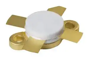
- Transistor Case Style: M174
- Operating Frequency Max: 175MHz
- Operating Frequency Min: -
- Drain Source Voltage Vds: 130V
- Operating Temperature Max: 200°C
- Continuous Drain Current Id: 20A
| Delivery and price | |
|---|---|
| Units per pack | 50 |
| Price | 47.6 € |
| Current stock | 500+ |
| Lead time | 7 days |
## **SD2941-10**

## HF/VHF/UHF RF power N-channel MOSFETs

**Datasheet** - **production data**

## **Features**

- Gold metallization

- Excellent thermal stability

- Common source configuration

- POUT = 175 W min. with 15 dB gain @ 175 MHz, 50 V

**==> picture [84 x 10] intentionally omitted <==**

**----- Start of picture text -----**<br>
M174 Epoxy sealed<br>**----- End of picture text -----**<br>


- POUT = 135 W typ. with 14 dB gain @ 123 MHz, 28 V

- Low R DS(on)

- Thermally enhanced packaging for lower junction temperatures

## **Figure 1. Pin connection**

1. Drain 4 1 2. Source 3. Gate 4. Source 3 2

- In compliance with the 2002/95/EC1 European directive

## **Description**

The SD2941-10 is a gold metalized N-channel MOS field-effect RF power transistor, intended for use in 28 V to 50 V dc large signal applications up to 230 MHz. It offers 25% lower R than the DS(on) industry standard, with 20% higher PSAT than ST's SD2931-10 device. The SD2941-10 is housed in the low thermal M174 non-pedestal package, offering 25% lower thermal resistance than the industry standard, thus rendering it the "best-in-class" transistor for ISM applications, where reliability and ruggedness are critical factor.

**Table 1. Device summary**

|**Order code**|**Marking**|**Base qty.**|**Package**|**Packaging(1)**|
|---|---|---|---|---|
|SD2941-10W|SD2941-10(1)|25 pcs|M174|Plastic tray|


1. For more details please refer to _Chapter 7: Marking, packing and shipping specifications_ .

1/17

August 2015 DocID11815 Rev 6

This is information on a product in full production.

_www.st.com_

**Contents**

**SD2941-10**

## **Contents**

|**1**|**Electrical data  . . . . . . . . . . . . . . . . . . . . . . . . . . . . . . . . . . . . . . . . . . . . . . 3**|
|---|---|
||1.1<br>Maximum rating  . . . . . . . . . . . . . . . . . . . . . . . . . . . . . . . . . . . . . . . . . . . . . 3|
|**2**|**Electrical characteristics  . . . . . . . . . . . . . . . . . . . . . . . . . . . . . . . . . . . . . 4**|
|**3**|**Impedance  . . . . . . . . . . . . . . . . . . . . . . . . . . . . . . . . . . . . . . . . . . . . . . . . . 6**|
|**4**|**Typical performance     . . . . . . . . . . . . . . . . . . . . . . . . . . . . . . . . . . . . . . . 7**|
|**5**|**Test circuit . . . . . . . . . . . . . . . . . . . . . . . . . . . . . . . . . . . . . . . . . . . . . . . . 10**|
|**6**|**Package information . . . . . . . . . . . . . . . . . . . . . . . . . . . . . . . . . . . . . . . . 13**|
|**7**|**Marking, packing and shipping specifications . . . . . . . . . . . . . . . . . . . 15**|
|**8**|**Revision history  . . . . . . . . . . . . . . . . . . . . . . . . . . . . . . . . . . . . . . . . . . . 16**|


2/17

DocID11815 Rev 6

**SD2941-10**

**Electrical data**

## **1 Electrical data**

## **1.1 Maximum rating**

## (TCASE = 25 ° C)

**Table 2. Absolute maximum rating**

|**Symbol**|**Parameter**|**Value**|**Unit**|
|---|---|---|---|
|V(BR)DSS<br>(1)|Drain source voltage|130|V|
|VDGR<br>(1)|Drain-gate voltage (RGS= 1MΩ)|130|V|
|VGS|Gate-source voltage|±40|V|
|ID|Drain current|20|A|
|PDISS|Power dissipation|389|W|
|TJ|Max. operating junction temperature|200|°C|
|TSTG|Storage temperature|-65 to +150|°C|


1. TJ = 150 °C

**Table 3. Thermal data**

||**Table 3. Thermal data**|||
|---|---|---|---|
|**Symbol**|**Parameter**|**Value**|**Unit**|
|RthJC|Junction to case thermal resistance|0.45|°C/W|


3/17

DocID11815 Rev 6

**SD2941-10**

**Electrical characteristics**

## **2 Electrical characteristics**

## (TCASE = 25 ° C)

**Table 4. Static**

||**Table 4. Static**|||||
|---|---|---|---|---|---|
|**Symbol**|**Test conditions**|**Min.**|**Typ.**|**Max.**|**Unit**|
|V(BR)DSS<br>(1)|VGS= 0 V<br>IDS= 100 mA|130|||V|
|IDSS|VGS= 0 V<br>VDS= 50 V|||50|mA|
|IGSS|VGS= 20 V<br>VDS= 0 V|||250|nA|
|VGS(Q)<br>(2)|VDS= 10 V<br>ID= 250 mA||||V|
|VDS(ON)|VGS= 10 V<br> ID= 10 A|||2.0|V|
|GFS|VDS= 10 V<br>ID= 5 A|5|6||mho|
|CISS|VGS= 0 V<br>VDS= 50 V<br>f = 1 MHz||415||pF|
|COSS|VGS= 0 V<br>VDS= 50 V<br> f = 1 MHz||236||pF|
|CRSS|VGS= 0 V<br>VDS= 50 V<br> f = 1 MHz||17||pF|


1. TJ = 150 ° C

2. VGS(Q) sorted with alpha/numeric code marked on unit.

**Table 5. Dynamic**

|**Symbol**|**Test conditions**|**Min.**|**Typ.**|**Max.**|**Unit**|
|---|---|---|---|---|---|
|POUT|VDD= 28 V IDQ= 250 mA f = 123 MHz||135|-|W|
||VDD= 50 V IDQ= 250 mA f = 175 MHz|175|200|||
|GPS|VDD= 28 V IDQ= 250 mA<br>POUT =135 W f = 123 MHz||14||dB|
||VDD= 50 V IDQ= 250 mA<br>POUT =175 W f = 175 MHz|14|15.8|||
|hD|VDD= 28 V IDQ= 250 mA POUT= 135 W f = 123 MHz||65||%|
||VDD= 50 V IDQ= 250 mA POUT= 175 W f = 175MHz|55|65|||
|Load<br>Mismatch|VDD= 50 V IDQ= 250 mA<br>POUT =175 W f = 175MHz<br>All phase angles|10:1|||VSWR|
||VDD= 28 V IDQ= 250 mA<br>POUT =135 W f = 123 MHz<br>All phase angles|25:1||||


4/17

DocID11815 Rev 6

**SD2941-10**

**Electrical characteristics**

**Table 6. VGS sorts**

|**Symbol**|**Value**|**Symbol**|**Value**|**Symbol**|**Value**|
|---|---|---|---|---|---|
|AA|1.5 - 1.6|E|2.4 - 2.5|P|3.3 - 3.4|
|BB|1.6 - 1.7|F|2.5 - 2.6|Q|3.4 - 3.5|
|CC|1.7 - 1.8|G|2.6 - 2.7|R|3.5 - 3.6|
|DD|1.8 - 1.9|H|2.7 - 2.8|S|3.6 - 3.7|
|EE|1.9 - 2.0|J|2.8 - 2.9|T|3.7 - 3.8|
|A|2.0 - 2.1|K|2.9 - 3.0|U|3.8 - 3.9|
|B|2.1 - 2.2|L|3.0 - 3.1|V|3.9 - 4.0|
|C|2.2 - 2.3|M|3.1 - 3.2|||
|D|2.3 - 2.4|N|3.2 - 3.3|||


5/17

DocID11815 Rev 6

**SD2941-10**

**Impedance**

## **3 Impedance**

## **Figure 2. Impedance data schematic**

**==> picture [230 x 139] intentionally omitted <==**

**----- Start of picture text -----**<br>
D<br>ZDL<br>Typical Input Typical Drain<br>Impedance Load Impedance<br>G<br>Zin<br>S<br>**----- End of picture text -----**<br>


**Table 7. Impedance data @ 28 V**

|**f**|**ZIN (**Ω**)**|**ZDL (100W)(**Ω**)**|**ZDL (140W)(**Ω**)**|
|---|---|---|---|
|123 MHz|1.2 - j 3.3|2.0 + j 1.4|2.0 + j 0.73|


**Table 8. Impedance data @ 50 V**

|**f**|**ZIN (**Ω**)**|**ZDL (**Ω**)**|
|---|---|---|
|30 MHz|1.7 - j 5.7|6.8 + j 0.9|
|175 MHz|1.2 - j 2.0|2.0 + j 2.4|


6/17

DocID11815 Rev 6

**SD2941-10**

**Typical performance**

## **4 Typical performance**

**Figure 3. Capacitance vs drain voltage**

## **Figure 4. Drain current vs gate voltage**

**==> picture [462 x 205] intentionally omitted <==**

**----- Start of picture text -----**<br>
10000<br>20<br>Tc=-20 °C<br>f =1MHz Tc=+25 °C<br>15<br>1000<br>Ciss<br>Coss 10 Tc=+80 °C<br>100 VDS = 10 V<br>5<br>Crss<br>10<br>0<br>0 10 20 30 40 50<br>2 2.5 3 3.5 4 4.5 5 5.5 6<br>VDS, DRAIN-SOURCE VOLTAGE (V)<br>VGS, GATE-SOURCE VOLTAGE (V)<br>C, CAPACITANCE (pF) ID, DRAIN CURRENT (A)<br>**----- End of picture text -----**<br>


**Figure 5. Maximum thermal resistance vs case temperature**

**Figure 6. Safe operating area**

**==> picture [462 x 205] intentionally omitted <==**

**----- Start of picture text -----**<br>
0.6 100<br>0.56<br>0.52<br>10<br>(1)<br>0.48<br>0.44<br>25 35 45 55 65 75 85 1<br>Tc, CASE TEMPERATURE (°C) 1 10 100 1000<br>Vds(V)<br>(1) Current in this area may be limited by Rds(on)<br>Ids(A)<br>RTH(j-c) (°C/W)<br>**----- End of picture text -----**<br>


7/17

DocID11815 Rev 6

**Typical performance**

**SD2941-10**

## **Figure 7. Power gain vs output power**

## **Figure 8. Efficiency vs output power**

**==> picture [462 x 219] intentionally omitted <==**

**----- Start of picture text -----**<br>
22 80<br>21<br>70<br>20 175 MHz<br>60<br>19 100 MHz<br>50<br>18<br>100 MHz<br>17 40<br>16<br>30<br>15 175 MHz<br>20<br>14<br>13 Vdd = 50V 10 Vdd = 50V<br>Idq = 250mA Idq = 250mA<br>12 0<br>0 25 50 75 100 125 150 175 200 225 250 275 0 25 50 75 100 125 150 175 200 225 250 275<br>Pout (W) Pout (W)<br>Gain (dB) Nd (%)<br>**----- End of picture text -----**<br>


**Figure 9. Input return loss vs output power**

**Figure 10. Gain and efficiency vs output power @ 28V and 100W load line**

**==> picture [462 x 219] intentionally omitted <==**

**----- Start of picture text -----**<br>
24 20 100<br>18 90<br>20<br>175 MHz 16 80<br>14 70<br>16<br>12 60<br>12 10 50<br>8 40<br>100 MHz<br>8<br>6 30<br>Gain Efficiency<br>4 20<br>4<br>Vdd = 50V 2 Freq = 123 MHz 10<br>Idq = 250mA Idq = 250mA<br>0 0 0<br>0 25 50 75 100 125 150 175 200 225 250 275 0 20 40 60 80 100 120 140 160<br>Pout (W) Output Power (W)<br>RTL (dB) Gain (dB)<br>Efficiency (%)<br>**----- End of picture text -----**<br>


8/17

DocID11815 Rev 6

**SD2941-10**

**Typical performance**

**Figure 11. Gain and efficiency vs output power @ 28V and 140W load line**

**==> picture [201 x 172] intentionally omitted <==**

**----- Start of picture text -----**<br>
20 100<br>18 90<br>16 80<br>14 70<br>12 60<br>10 50<br>8 40<br>6 30<br>Gain Efficiency<br>4 20<br>2 Freq = 123 MHz 10<br>Idq = 250mA<br>0 0<br>0 20 40 60 80 100 120 140 160<br>Output Power (W)<br>Gain (dB)<br>Efficiency (%)<br>**----- End of picture text -----**<br>


9/17

DocID11815 Rev 6

**SD2941-10**

**Test circuit**

## **5 Test circuit**

## **Figure 12. 30 MHz test circuit schematic (engineering test circuit)**

**==> picture [395 x 209] intentionally omitted <==**

_Note:_

_All dimension are in inches._

**Table 9. 30 MHz test circuit component part list**

||**Table 9. 30 MHz test circuit componentpart list**|
|---|---|
|**Symbol**|**Description**|
|T2|1:4 transformer, 25 Ω semi-rigid coax.141 OD 6” Long|
|FB1|Toroid X 2, 0.5” OD.312” ID 850µ 2 turns|
|FB2, FB3|VK200|
|FB4|Shield bead, 1” OD 0.5” ID 850µ 3 Turns|
|L1|1/4 Wave Choke, 50W Semi-rigid coax.141 OD 12” Long|
|PCB|0.62” woven fiberglass, 1 oz. copper, 2 sides,εr = 2.55|
|R1, R3|470 Ω 1 W chip resistor|
|R2|360 Ω 1/2 W resistor|
|R4|20 KΩ 10 turn potentiometer|
|R5|560 Ω 1 W resistor|
|C1, C11|470 pF ATC chip cap|
|C2|43 pF ATC chip cap|
|C3, C8, C9|Arco 404, 12-65 pF|
|C4|Arco 423, 16-100 pF|
|C5|120 pF ATC chip cap|
|C6|0.01μF ATC chip cap|
|C7|30 pF ATC chip cap|


10/17

DocID11815 Rev 6

**SD2941-10**

**Test circuit**

**Table 9. 30 MHz test circuit component part list (continued)**

|**Symbol**|**Description**|
|---|---|
|C10<br>91 pF|ATC chip cap|
|C12, C15<br>1200|pF ATC chip cap|
|C13, C14,C16, C17 0.01|mF / 500 V chip cap|
|C18<br>10 m|F 63 V electrolytic capacitor|


## **Figure 13. 175 MHz test circuit photomaster**

**==> picture [375 x 242] intentionally omitted <==**

**----- Start of picture text -----**<br>
6.4 inches<br>4 inches<br>**----- End of picture text -----**<br>


11/17

DocID11815 Rev 6

**SD2941-10**

**Test circuit**

**==> picture [145 x 11] intentionally omitted <==**

**----- Start of picture text -----**<br>
Figure 14. 175 MHz test circuit<br>**----- End of picture text -----**<br>


**==> picture [436 x 224] intentionally omitted <==**

12/17

DocID11815 Rev 6

**SD2941-10**

**Package information**

## **6 Package information**

In order to meet environmental requirements, ST offers these devices in different grades of ECOPACK[®] packages, depending on their level of environmental compliance. ECOPACK[®] specifications, grade definitions and product status are available at: _www.st.com_ . ECOPACK[®] is an ST trademark.

## **Figure 15. M174 package dimensions**

**==> picture [254 x 283] intentionally omitted <==**

13/17

DocID11815 Rev 6

**Package information**

**SD2941-10**

**Table 10. M174 (.500 DIA 4/L N/HERM W/FLG)**

||**Table 10. M174(.500 DIA 4/L**|**Table 10. M174(.500 DIA 4/L**|**Table 10. M174(.500 DIA 4/L**|**N/HERM W/FLG)**|**N/HERM W/FLG)**|**N/HERM W/FLG)**|
|---|---|---|---|---|---|---|
|**DIM.**|**mm.**|||**inch**|||
||**min.**|**typ.**|**max**|**min.**|**typ.**|**max**|
|A|5.56||5.584|0.219||0.230|
|B||3.18|||0.125||
|C|6.22||6.48|0.245||0.255|
|D|18.28||18.54|0.720||0.730|
|E||3.18|||0.125||
|F|24.64||24.89|0.970||0.980|
|G|12.57||12.83|0.495||0.505|
|H|0.08||0.18|0.003||0.007|
|I|2.11||3.00|0.083||0.118|
|J|3.81||4.45|0.150||0.175|
|K|||7.11|||0.280|
|L|25.53||26.67|1.005||1.050|
|M|3.05||3.30|0.120||0.130|


14/17

DocID11815 Rev 6

**SD2941-10**

**Marking, packing and shipping specifications**

## **7 Marking, packing and shipping specifications**

**Table 11. Packing and shipping specifications**

|**Order code**|**Packaging**|**Pcs per**<br>**tray**|**Dry pack**<br>**humidity**|**VGScode**|**Lot code**|
|---|---|---|---|---|---|
|SD2941-10W|Plastic tray|25|< 10%|Not mixed|Not mixed|


## **Figure 16. Marking layout**

**==> picture [244 x 244] intentionally omitted <==**

**----- Start of picture text -----**<br>
SD2941-10<br>**----- End of picture text -----**<br>


**Table 12. Marking specifications**

||**Table 12. Marking specifications**|
|---|---|
|**Symbol**|**Description**|
|W|Wafer process code|
|X|VGSsort|
|CZ|Assembly plant|
|xxx|Last 3 digit of diffusion lot|
|VY|Diffusion plant|
|MAR|Country of origin|
|CZ|Test and finishing plant|
|y|Assembly year|
|yy|Assembly week|


15/17

DocID11815 Rev 6

**SD2941-10**

**Revision history**

## **8 Revision history**

**Table 13. Document revision history**

|||**Table 13. Document revision history**|
|---|---|---|
|**Date**|**Revision**|**Changes**|
|15-Nov-2005|1|Initial release|
|06-Apr-2006|2|Complete version|
|13-Apr-2006|3|VDS(ON)updated|
|19-Oct-2011|4|Inserted_Section 7: Marking, packing and shipping specifications_.<br>Minor text changes in the title and description on the coverpage.|
|04-Aug-2014|5|Added performances at 28 V.|
|14-Aug-2015|6|Updated_Table 2.: Absolute maximum rating_.<br>Minor text changes.|


16/17

DocID11815 Rev 6

**SD2941-10**

## **IMPORTANT NOTICE – PLEASE READ CAREFULLY**

STMicroelectronics NV and its subsidiaries (“ST”) reserve the right to make changes, corrections, enhancements, modifications, and improvements to ST products and/or to this document at any time without notice. Purchasers should obtain the latest relevant information on ST products before placing orders. ST products are sold pursuant to ST’s terms and conditions of sale in place at the time of order acknowledgement.

Purchasers are solely responsible for the choice, selection, and use of ST products and ST assumes no liability for application assistance or the design of Purchasers’ products.

No license, express or implied, to any intellectual property right is granted by ST herein.

Resale of ST products with provisions different from the information set forth herein shall void any warranty granted by ST for such product.

ST and the ST logo are trademarks of ST. All other product or service names are the property of their respective owners.

Information in this document supersedes and replaces information previously supplied in any prior versions of this document.

© 2015 STMicroelectronics – All rights reserved

17/17

DocID11815 Rev 6
Updated at March 21, 2026
STMicroelectronics is a global leader in the semiconductor industry, recognized for developing highly integrated, energy-efficient solutions that power modern electronics. With a strong focus on innovation, ST provides a comprehensive portfolio of microelectronics that address the demanding requirements of industrial, automotive, communications, and consumer applications. Our extensive selection of STMicroelectronics components is built around a robust lineup of discrete semiconductors and circuit protection devices. We offer a wide variety of single MOSFETs, Schottky diodes, and fast and ultrafast recovery rectifier diodes, designed to deliver exceptional efficiency and thermal performance in power management and conversion systems. For robust circuit protection, our inventory features hundreds of transient voltage suppressors and TVS diodes that safeguard sensitive electronic components against destructive voltage spikes. In addition to core power discretes like TRIACs, SCRs, bipolar transistors, and single IGBTs, our STMicroelectronics range includes specialized integrated passive filters and MEMS sensors. Furthermore, ST offers advanced integrated passive devices, such as baluns and RF filters, which utilize high-quality monolithic RF IPD processes on glass or high-resistance silicon substrates. These components provide competitive cost structures, reduced power losses, and simplified RFIC-to-antenna matching, ensuring optimal system performance and delivering the reliability required for next-generation wireless and power designs.
About Novapart
Novapart is a B2B electronic component broker specialising in stock shortages and cost reduction. We source hard-to-find parts and identify compliant alternatives across a catalogue of 540,000+ components from 500+ manufacturers.
Learn more →Stock Shortage Specialist
When a component is unavailable, discontinued or has an unacceptable lead time, we tap into our network of vetted European and Asian distributors to source what you need — without compromising on quality or traceability.
Request a quote →Compliant Alternatives
We identify pin-to-pin, electrically equivalent substitutes that meet the same certifications (RoHS, AEC-Q100, REACH) as your original specification — validated against datasheets, not just part numbers. Often at a lower cost.
BOM Analysis service →