
Image not available
Illustrative purposes only

SCM0100200
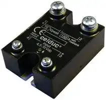
MOSFET Relay, DC, 200 V, 100 A, Hockey Puck, Panel Mount
⚠️ Reference pricing provided. In case of supply shortages, we will connect you with our trusted procurement partners to ensure your project's continuity.
- Manufacturer: CELDUC
- Product type: MOSFET Solid State Relays
- Contact Configuration:-; Load Current:100A; Relay Terminals:Screw; Load Voltage Max:200VDC; On State Resistance Max:0.022ohm; Isolation Voltage:4kV; Forward Current If:42mA; Product Ran
- SVHC: Lead (27-Jun-2024)
- Load Type: DC
- Contact Form: -
- Load Current: 100A
- Product Range: SCM Series
- Relay Mounting: Panel Mount
- Relay Terminals: Screw
- Load Voltage Max: 200V
- Isolation Voltage: 4kV
- Forward Current If: 42mA
- I/O Capacitance Typ: -
- On State Resistance Max: 0.022ohm
- MOSFET Relay Package Style: Hockey Puck
- Off State Leakage Current Max: -
| Delivery and price | |
|---|---|
| Units per pack | 1 |
| Price | 226.6 € |
| Current stock | 10+ |
| Lead time | 30 days |
Datasheet

**S/CON/SCM0100200/F/19/12/14** **Page 1/5 GB** ## MOSFET BASED DC SOLID STATE RELAY ## SCM0100200 - Latest MOSFET technology generation. - Ultra low on-state resistance. - New innovative isolated driver ensuring fast power transistor turn on and off therefore low power transient. - Ultra low output leakage current - Low control current consumption > Control voltage range 4.5-32VDC Max. output peak 200VDC voltage Nom. load current 100ADC with heatsink - Triggered control input to avoid linear control risks - Low conducted and radiated disturbances **==> picture [508 x 290] intentionally omitted <==** **----- Start of picture text -----**<br> Control input In & case / Out Dimensions<br>Load voltage range Load current range voltage range Insulation Connections (WxHxD) Weight<br>Depends on protection clamping voltage (with heatsink)0 to 100A 4.5-32VDC 4kV M3 round tabs M5 round tabs 44.5 x 58.2 x 27 (mm) 100g<br>HIGH SIDE WIRING DIAGRAM LOW SIDE WIRING DIAGRAM<br>Fig. 1 Fig. 2<br>(Load connected to “-“) (Load connected to “+”)<br>PowerDC+ ControlSupply- + DC Mains - T ‘. J poweri]Supply<br>Please consult us Please consult us<br>to select the right to select the<br>la =| protective C1 lV aN control right protective<br>| i. components C1, °F ve On-Of f components C1,<br>D1 & D2. D1 & D2.<br>l c Tee (eeD1 eTy The red paths aru D4D Gi The red paths<br>On -O ff AV 000°" (C1/D1/D2) must gb2 (2) 6) (C1/D1/D2) must<br>control | © oh or be as short as or @) | be as short as<br>", ><br>possible ! possible !<br>w s <a<br>if if<br>Fig. 3 INTERNAL DIAGRAM<br>**----- End of picture text -----**<br> Fig. 3 ## _Proud to serve you_ **==> picture [231 x 53] intentionally omitted <==** **----- Start of picture text -----**<br> celduc®<br>**----- End of picture text -----**<br> Data given at Tambient=40°C and subject to modification without previous notice **r e l a i s** **celduc® r e l a i s** **S/CON/SCM0100200/F/19/12/14** **Page 2/5 GB** ||||CONTROL INPUT CHARACTERISTICS|CONTROL INPUT CHARACTERISTICS|CONTROL INPUT CHARACTERISTICS| |---|---|---|---|---|---| ||||||| ||||||| ||||||| |INPUT CIRCUIT|CHARACTERISTIC|LABEL|VALUE||INFO.| ||Control voltage range|Uc|4.5 – 32VDC||| ||Current consumption|Ic|25 – 42mADC for control voltage range||See fig. 5| ||Typical turn on voltage|Ucontyp|4.3V||| ||Min. releasing voltage|Ucoffmin|1VDC||| ||Typical releasing voltage|Ucofftyp|3.5V||| ||Max. input voltage|Ucmax|32VDC||| ||Max. reverse voltage|-Ucmax|32VDC||| ||Max. reverse leakage current|-Icmax|100µA||| ||Input impedance|Re|Current limitation||See fig. 5| ||||||| ||||POWER OUTPUT CHARACTERISTICS||| ||||||| ||||||| ||||||| |POWER CIRCUIT|CHARACTERISTIC|LABEL|VALUE||INFO.| ||Mains voltage range|Ue|Depends on protection clamping voltage (D1)||| ||Non-repetitive peak voltage|Utp|200V||| ||Overvoltage protection|D1|Not integrated<br>A voltage clamping mean must be connected across the<br>terminals 1 & 2 (see fig 1 & 2)||See Instruction<br>sheet for selective<br>the right<br>protective<br>components| ||Reverse voltage (internal diode)|-Ut|1,6V||@Ie=-100A<br>@Uc=0| ||Max. repetitive avalanche current|Iep|100A||Pulse width<br>limited by Tj<br>max| ||Max. single pulse avalanche energy|Eep|750mJ||@Ut=50V<br>@Ie=Iep| ||Max. repetitive pulse avalanche<br>energy|Eep|58mJ||@Ie=56A| ||Maximum nominal currents|Ie|Resistive|Motor|See fig. 7<br>Values with<br>heatsink| ||||100A|Please consult us|| ||Non-repetitive peak overload<br>current|Iepeak|380A||See fig. 8| ||Min. load current|Iemin|0mA||| ||Max. leakage current|Ielk|250µADC||@Utp @Tjmax| ||Max. on-state resistance|RDSon|22m||@Iemax @Tjmax| ||Typ. output capacitance|Cout|1.5nF||| ||Junction/case thermal resistance<br>per power element|Rthjc|0.4K/W||Total = 2<br>power<br>elements| ||Built-in heatsink thermal<br>resistance verticallymounted|Rthra|8K/W||@Tra=60°C| ||Heatsink thermal time constant|Tthra|10min||@Tra=60°C| ||Control inputs/power outputs<br>insulation voltage|Uimp|4kV||| ||Inputs/case insulation voltage|Uimp|4kV||| ||Outputs/case insulation voltage|Uimp|4kV||| ||Isolation resistance|Rio|1G||| ||Isolation capacitance|Cio|<8pF||| ||Maximum junction temperature|Tjmax|175°C||| ||Storage ambient temperature|Tstg|-40->+100°C||| ||Operating ambient temperature|Tamb|-40->+90°C||See fig. 7| ||Max. case temperature|Tc|100°C||| **celduc® r e l a i s** **S/CON/SCM0100200/F/19/12/14** **Page 3/5 GB** ## TIME CHARACTERISTICS **==> picture [516 x 133] intentionally omitted <==** **----- Start of picture text -----**<br> Fig. 4 TIME DIAGRAMS<br>**----- End of picture text -----**<br> |Fig. 4|TIME DIAGRAMS|TIME DIAGRAMS|TIME DIAGRAMS|TIME DIAGRAMS|TIME DIAGRAMS|TIME DIAGRAMS|TIME DIAGRAMS|TIME DIAGRAMS|TIME DIAGRAMS|TIME DIAGRAMS|TIME DIAGRAMS| |---|---|---|---|---|---|---|---|---|---|---|---| ||||||||||||| ||||||||||||| ||||||||||||| ||||||||||||| ||||||||||||| ||||||||||||| ||||||||||||| |TIME CHARACT.|CHARACTERISTIC||||LABEL|VALUE|||||INFO.| ||Turn on time||||ton|10µs (1.2µs typical)|||||| ||Turn on delay||||tdon|600µs (500µs typical)|||||| ||Turn off time||||toff|10µs (1µs typical)|||||| ||Turn off delay||||tdoff|100µs (60µs typical)|||||| ||Max. On-Off frequency||||F(on-off)|700Hz|||||| ||||||||||||| |||||||GENERAL INFORMATION|||||| ||||||||||||| ||||||||||||| ||||||||||||| |CONNEC-<br>TIONS|Connections|||||Power|||Control||| ||Screwdriver advised|||||Philips™ NR2|||Philips™ NR1||| ||Min and max tightening torque|||||1.8 N.m|||0.8 N.m||| ||Insulated crimp terminals (round<br>tabs, eyelet type)|||||M5|||M3||| ||||||||||||| |MISC.|Display|||||Green LED<br>(indicates relayhas switched ON)|||||| ||Housing|||||UL94V0|||||| ||Mounting|||||2 screws (M4x12mm)|||||See mounting<br>sheet| ||Noise level|||||No audible noise|||||| ||Weight|||||100g|||||| ||||||||||||| |||||||STANDARDS|||||| ||||||||||||| ||||||||||||| ||||||||||||| |GENERAL|Standards|||||IEC60947-1|||||| ||Protection level|||||IP00|||||| ||Protection against direct touch|||||None|||||| ||CE marking|||||Yes|||||| ||UL, cULUS|||||Yes|||||| ||||||||||||| |E.M.C.<br>IMMUNITY|TYPE OF TEST||||STANDARD|LEVEL|||||EFFECT| ||E.S.D. (Electrostatic discharges)||||EN61000-4-2|Pending|||||?| ||Radiated electromagnetic fields||||EN61000-4-3|Pending|||||?| ||Fast transients bursts||||EN61000-4-4|4kV coupling by clamp on the input side and direct for power side|||||No effect| ||Electric chocks||||EN61000-4-5|1kV direct coupling on the input side (pending for power side)|||||?| ||Voltage drop||||EN61000-4-11|-|||||| ||||||||||||| |E.M.C.<br>EMISSION|Radiated and conducted<br>disturbances||||NFEN55011|Pending|||||| **celduc® r e l a i s** **S/CON/SCM0100200/F/19/12/14** **Page 4/5 GB** ## CHARACTERISTIC CURVES **==> picture [516 x 516] intentionally omitted <==** **----- Start of picture text -----**<br> Fig. 5 INPUT CHARACTERISTIC Fig. 6 ON RESISTANCE VS TEMPERATURE<br>Ic (mADC) RDSon<br>25<br>45 (mOhms)<br>40<br>20<br>35<br>30 @25°C 15<br>25<br>20 10<br>15<br>10 5<br>5<br>0<br>0<br>-50 0 50 100 150<br>0 2 4 6 8 10 12 14 16 18 20 22 24 26 28 30 32 Junction Temperature (°C)<br>Uc (VDC)<br>Fig. 7 POWER DISSIPATED AND LOAD CURRENT LIMIT VS TEMPERATURE<br>Permanent current Please refere to the installation notice for Power dissipated<br>Ie (ARMS) precautions about mounting the device on a heatsink. (W)<br>110 266<br>1.3K/W 1.2K/W 1.1K/W 0.9K/W 0.75K/W 0.55K/W 0.3K/W 0.2K/W 0.1K/W<br>100 220<br>90 178<br>80 141<br>70 108<br>60 79.2<br>50 55<br>40 35.2<br>30 19.8<br>20 8.8<br>10 2.2<br>8K/W 4K/W 2.4K/W 2.2K/W 2.1K/W 1.95K/W 1.5K/W<br>0<br>0<br>0 10 20 30 40 50 60 70 80 90 100 110<br>Ambient temperature (°C)<br>8K/W = No Heatsink 4K/W = No reference 2.4K/W = WF152100 2.2K/W = WF262100 2.2K/W = WF151200<br>2.1K/W = WF210000 1.95K/W = WF191100 1.5K/W = WF141100 1.3K/W = WF129100 1.2K/W = WF121000<br>1.1K/W = WF131100 0.9K/W = WF092000 0.9K/W = WF115100 0.7K/W = WF070000 0.55K/W = WF050000<br>0.3K/W = WF031100 0.2K/W = WF020000 0.1K/W = No reference<br>**----- End of picture text -----**<br> **==> picture [516 x 477] intentionally omitted <==** **----- Start of picture text -----**<br> Permanent current Please refere to the installation notice for Power dissipated<br>Ie (ARMS) precautions about mounting the device on a heatsink. (W)<br>110 266<br>1.3K/W 1.2K/W 1.1K/W 0.9K/W 0.75K/W 0.55K/W 0.3K/W 0.2K/W 0.1K/W<br>100 220<br>90 178<br>80 141<br>70 108<br>60 79.2<br>50 55<br>40 35.2<br>30 19.8<br>20 8.8<br>10 2.2<br>8K/W 4K/W 2.4K/W 2.2K/W 2.1K/W 1.95K/W 1.5K/W<br>0<br>0<br>0 10 20 30 40 50 60 70 80 90 100 110<br>Ambient temperature (°C)<br>8K/W = No Heatsink 4K/W = No reference 2.4K/W = WF152100 2.2K/W = WF262100 2.2K/W = WF151200<br>2.1K/W = WF210000 1.95K/W = WF191100 1.5K/W = WF141100 1.3K/W = WF129100 1.2K/W = WF121000<br>1.1K/W = WF131100 0.9K/W = WF092000 0.9K/W = WF115100 0.7K/W = WF070000 0.55K/W = WF050000<br>0.3K/W = WF031100 0.2K/W = WF020000 0.1K/W = No reference<br>Fig. 8 CURRENT OVERLOAD CHARACTERISTIC<br>Ie 400<br>(A)380360 Non repetitive<br>340 on-state (no switching)<br>320300 max. peak current<br>280 vs<br>260240 overload pulse duration<br>220<br>200<br>180<br>160<br>140<br>120<br>100<br>80<br>60<br>40<br>20<br>0<br>0,1 1 10 100 1000<br>Pulse duration (ms)<br>**----- End of picture text -----**<br> **celduc®** **S/CON/SCM0100200/F/19/12/14** **r e l a i s** **Page 5/5 GB** **==> picture [516 x 366] intentionally omitted <==** **----- Start of picture text -----**<br> DIMENSIONS AND ACCESSORIES<br>rr<br>Fig. 9 DIMENSIONS<br>|<br>28<br>±0,5<br>22.8<br>28<br>19.6 Ø4.7 M5<br>an -- Ow No —D VIN<br>1+ 2-<br>|<br>|<br>|<br>C| 4- 3+<br>a<br>: ame<br>25.4<br>25.8<br>| Am ch<br>44. ae 5 M3<br>TOLERANCES: [±] 0.3<br>Fig.<br>ACCESSORIES<br>10 |<br>58.2 43.2 47.6<br>7.5<br>5.1<br>**----- End of picture text -----**<br> ## PROTECTIVE COVER 1K470000 **celduc® www.celduc.com r e l a i s** ~~gs~~ **5 Rue Ampère B.P. 30004 42290 SORBIERS - FRANCE E-Mail : celduc-relais@celduc.com Fax +33 (0) 4 77 53 85 51 Service Commercial France Tél. : +33 (0) 4 77 53 90 20 Sales Dept.For Europe Tel. : +33 (0) 4 77 53 90 21 Sales Dept. Asia : Tél. +33 (0) 4 77 53 90 19** **www.celduc.com**
Updated at June 3, 2026
About Novapart
Novapart is a B2B electronic component broker specialising in stock shortages and cost reduction. We source hard-to-find parts and identify compliant alternatives across a catalogue of 410,000+ components from 500+ manufacturers.
Learn more →Stock Shortage Specialist
When a component is unavailable, discontinued or has an unacceptable lead time, we tap into our network of vetted European and Asian distributors to source what you need — without compromising on quality or traceability.
Request a quote →Compliant Alternatives
We identify pin-to-pin, electrically equivalent substitutes that meet the same certifications (RoHS, AEC-Q100, REACH) as your original specification — validated against datasheets, not just part numbers. Often at a lower cost.
BOM Analysis service →