
Image not available
Illustrative purposes only

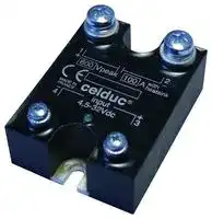
SCI0100600
Solid State Relay, 100 A, 600 VDC, Panel Mount, Screw
⚠️ Reference pricing provided. In case of supply shortages, we will connect you with our trusted procurement partners to ensure your project's continuity.
- Manufacturer: CELDUC
- Product type:
- Contact Configuration:-; Load Current:100A; Operating Voltage Max:600VDC; Relay Mounting:Panel; Relay Terminals:Screw; Switching Mode:-; Operating Voltage Min:0VDC; Control Voltage Mi
- SVHC: Lead (27-Jun-2024)
- Load Current: 100A
- Product Range: SCI Series
- Relay Mounting: Panel Mount
- Switching Mode: -
- Relay Terminals: Screw
- Control Voltage Max: 32VDC
- Control Voltage Min: 4.5VDC
- Contact Configuration: -
- Operating Voltage Max: 600VDC
- Operating Voltage Min: 0VDC
| Delivery and price | |
|---|---|
| Units per pack | 1 |
| Price | 464.2 € |
| Current stock | 10+ |
| Lead time | 30 days |
Datasheet

**S/CON/SCI0100600/D/19/12/14** **Page 1/5 UK** **==> picture [359 x 23] intentionally omitted <==** **----- Start of picture text -----**<br> —(«celdyue?|<br>**----- End of picture text -----**<br> ## IGBT BASED DC SOLID-STATE RELAY **==> picture [96 x 13] intentionally omitted <==** **----- Start of picture text -----**<br> SCI0100600<br>**----- End of picture text -----**<br> - Latest high voltage IGBT technology generation. - New innovative isolated driver ensuring fast power transistor turn on and off therefore low power transient. - Ultra low output leakage current - Low control current consumption - Triggered control input to avoid linear control risks - Low conducted and radiated disturbances > Control voltage range 4.5-32VDC Max transient peak 600V voltage Advised max. DC (Depends on protection clamping Mains peak voltage voltage) Max. Load Current 100ADC (with heatsink) **==> picture [509 x 292] intentionally omitted <==** **----- Start of picture text -----**<br> DC Mains Control input In & case / Out Dimensions<br>voltage range Load current range voltage range Insulation Connections (WxHxD) Weight<br> (Depends on protection 0 to 100A M3 round tabs 44.5 x 58.2 x 27<br>clamping voltage) (with heatsink) 4.5-32VDC 4kV M5 round tabs (mm) 100g<br>HIGH SIDE WIRING DIAGRAM LOW SIDE WIRING DIAGRAM<br>Fig. 1 Fig. 2<br>(Load connected to “-“) (Load connected to “+”)<br>DC Control DC Control<br>Power Supply Power Supply<br>Please consult<br>+ - + DC Mains - T ‘J + -<br>Please consult us us to select the<br>le I , Ue to select the right le J. Ue on -o ff right<br>protective protective<br>components C1, components<br>| la =I] C1 (2e) cont rol<br>D1 & D2. C1, D1 & D2.<br>Ic Uc >)(@) (0J D1 o r tThha ." (C1/D1/D2) must The red paths id j ry et orD4 a, Uc The red paths (C1/D1/D2)<br>Oconntr -O ffol | (s\oh iy ory be as short as or. D2 es)f ) (o) | must be as<br>possible ! short as<br>=o 220"<br>possible !<br>TT iti<br>Fig. 3 INTERNAL DIAGRAM<br>**----- End of picture text -----**<br> ## _Proud to serve you_ **==> picture [231 x 53] intentionally omitted <==** **----- Start of picture text -----**<br> celduc®<br>**----- End of picture text -----**<br> Data given at Tambient=25°C and subject to modification without previous notice **r e l a i s** **celduc® r e l a i s** **S/CON/SCI0100600/D/19/12/14** **Page 2/5 UK** ## CONTROL INPUT CHARACTERISTICS ||CHARACTERISTIC|LABEL|VALUE|INFO.|Fig. 4|CONTROL CURRENT<br>vs. CONTROLVOLTAGE| |---|---|---|---|---|---|---| |INPUT CIRCUIT|Nom. Control voltage|Ucnom|12-24VDC||**0**<br>**5**<br>**10**<br>**15**<br>**20**<br>**25**<br>**30**<br>**35**<br>**40**<br>**45**<br>**0**<br>**Ic (mAD**|~~**@25°C**~~<br>**2**<br>**4**<br>**6**<br>**8**<br>**10**<br>**12**<br>**14**<br>**16**<br>**18**<br>**20**<br>**22**<br>**24**<br>**26**<br>**28**<br>**30**<br>**32**<br>**Uc (VDC)**<br>**C)**| ||Nom. Control current|Icnom|35mADC|||| ||Controlvoltagerange|Uc|4.5–32VDC|typical=4.3V||| ||Control current<br>consumption|Ic|25 – 42mADC|See curve||| ||Releasing control voltage|Ucoffmax|1VDC|Typical= 3.5V||| ||Max. reverse control<br>voltage|-Ucmax|32VDC|-Icmax <100µA||| ||Input impedance|Rin|Current<br>limitation|See curve||| ## TIME CHARACTERISTICS |TIME CHARACT.|CHARACTERISTIC|LABEL|VALUE||||||| |---|---|---|---|---|---|---|---|---|---| ||Turn on time|ton|10µs||||||| ||Turn on delay|tdon|600µs||||||| ||Turn off time|toff|10µs||||||| ||Turn off delay|tdoff|100µs||||||| ||Max. On-Off frequency|F(on-off)|700Hz||||||| ## POWER OUTPUT CHARACTERISTICS ## |POWER CIRCUIT|CHARACTERISTIC|LABEL|LABEL|VALUE|VALUE|INFO.| |---|---|---|---|---|---|---| ||Mains voltage range|Ut|Ue|Min = VCEsat<br>(Max Advised = 350VDC)||Depends on protection<br>clamping voltage (D1)| ||Non-repetitive peak voltage|Utp||600V||| ||Overvoltage protection|D1||Not integrated<br>A voltage clamping mean must be connected across the<br>terminals 1 & 2 (see fig1 & 2)||Please consult us to select<br>the right protective<br>components| ||Off-state max reverse voltage drop<br>(internal diode)|-Ut||1.4V||@Ie=100A| ||Maximum nominal currents|Ie max||Resistive|Motor|See fig. 9| |||||100A|Please contact us|| ||Max. non-repetitive non-switched<br>peak current|Iepeak||550A||@Tc=100°C @Tj=175°C<br>@Utp(See fig. 8)| ||Min. load current|Iemin||0mA||@Tj=25°C| ||Max. leakage current|Ielk max||1mA||@Utp @Tjmax| ||Voltage drop : Resistance|rt||6.4m||@Tj=125°C| ||Voltage drop : Voltage|vt||0.8V||@Tj=125°C| ||Max. on-state voltage drop<br>(Vcesat = vt + rt . Ie)|VCEsat||1.35V@Tj=25°C|1.45V@Tj=125°C|@Iemax| ||Typ. output capacitance|Cout||300pF||@Utp| ||Junction/case thermal resistance|Rthjc||0.385K/W||| ||Built-in heatsink thermal resistance<br>verticallymounted|Rthra||10K/W||@Tra=75°C| ||Heatsink thermal time constant|Tthra||10 minutes||@Tra=60°C| ||Control inputs / power outputs / case<br>insulation voltage|Uimp||4kV||| ||Isolation resistance / capacitance|Rio / Cio||1G<8pF||| ||Maximumjunction temperature|Tjmax||Steadystate = 125°C|Transient = 175°C|| ||Storage ambient temperature|Tstg||-40->+100°C||| ||Operatingambient temperature|Tamb||-40->+90°C||See fig. 9| ||Max. case temperature|Tc||100°C||| **celduc® r e l a i s** **S/CON/SCI0100600/D/19/12/14** **Page 3/5 UK** ## OUTPUT SWITCH CHARACTERISTIC CURVES **==> picture [516 x 696] intentionally omitted <==** **----- Start of picture text -----**<br> REVERSE VOLTAGE DROP<br>Fig. 5 VOLTAGE DROP VS LOAD CURRENT Fig. 6<br>VS REVERSE CURRENT<br>140<br>-Ie (A)<br>Ie (A) 200<br>120<br>100 150<br>80<br>100<br>60 Tj = 25°C<br>Tj = 125°C Tj=125°C<br>40<br>Tj = 175°C 50<br>20<br>VCEsat (V) -Ut (V)<br>0 0<br>0 0,2 0,4 0,6 0,8 1 1,2 1,4 1,6 1,8 2 0 0,5 1 1,5 2<br>POWER ELEMENT TRANSIENT THERMAL IMPEDANCE ON-STATE PEAK OVERLOAD CURRENT vs. PULSE<br>Fig. 7 Fig. 8<br>vs. PULSE DURATION DURATION<br>0,18 Zthjc (K/W) 700<br>Ie (Apk)<br>0,16 600<br>Non-repetitive D=1% (Tc=100°C, Tjmax=175°C)<br>0,14<br>500<br>0,12<br>400<br>0,1 D=50%<br>0,08 D=20% 300<br>D=10%<br>0,06 200<br>D=5%<br>0,04 D=2%<br>100<br>0,02 D=1% Repetitive D=50%(Tc=100°C, Tjmax=125°C)<br>Single pulse 0<br>0 0,0001 0,001 0,01 0,1 Pulse 1<br>0,0001 0,001 0,01 0,1 t (s) 1 Duration (s)<br>Fig. 9 POWER DISSIPATED AND LOAD CURRENT LIMIT VS TEMPERATURE<br>Permanent current Please refer to the installation notice for precautions about Power dissipated<br>Ie (ARMS) mounting the device on a heatsink. Pd (W)<br>110 165<br>2.2K/W 2.1K/W 1.2K/W 1.1K/W 0.9K/W 0.75K/W 0.55K/W 0.3K/W 0.2K/W 0.1K/W<br>100 144<br>90 123<br>80 105<br>70 87<br>60 70.9<br>50 55.9<br>40 42.2<br>30 29.7<br>20 18.5<br>10 8.64<br>8K/W 4K/W<br>0 0<br>0 10 20 30 40 50 60 70 80 90 100 110<br>Ambient temperature (°C)<br>10K/W = No Heatsink / 1LD12020 4K/W = 150x150x3mm aluminium sheet 2.2K/W = WF262100 / WF151200<br>2.1K/W = WF210000 1.2K/W = WF121000 1.1K/W = WF131100 0.9K/W = WF115100 0.75K/W = WF070000<br>0.55K/W = WF050000 0.3K/W = WF031100 0.2K/W = No reference 0.1K/W = No reference<br>**----- End of picture text -----**<br> **celduc® r e l a i s** **S/CON/SCI0100600/D/19/12/14** **Page 4/5 UK** ||||GENERAL INFORMATION|GENERAL INFORMATION|GENERAL INFORMATION| |---|---|---|---|---|---| ||||||| ||||||| ||||||| |CONNEC-<br>TIONS|Connections||Power|Control|| ||Screwdriver advised||Philips™ NR2|Philips™ NR1|| ||Min and max tightening torque||1.8 N.m|0.8 N.m|| ||Insulated crimp terminals (round<br>tabs, eyelet type)||M5|M3|| ||||||| |MISC.|Display||Green LED<br>(indicates thepower element is controlled)||| ||Housing||UL94V0||| ||Mounting||2 screws (M4x12mm)||See mounting<br>sheet| ||Noise level||No audible noise||| ||Weight||100g||| ||||||| ||||STANDARDS||| ||||||| ||||||| ||||||| |GENERAL|Standards||IEC60947-1||| ||Protection level||IP00||| ||Protection against direct touch||None||| ||CE marking||Yes||| ||UL, cULUS||Yes||| ||||||| |E.M.C.<br>IMMUNITY|TYPE OF TEST|STANDARD|LEVEL||EFFECT| ||E.S.D. (Electrostatic discharges)|EN61000-4-2|Pending||?| ||Radiated electromagnetic fields|EN61000-4-3|Pending||?| ||Fast transients bursts|EN61000-4-4|Pending||?| ||Electric chocks|EN61000-4-5|Pending||?| ||Voltage drop|EN61000-4-11|-||| ||||||| |E.M.C.<br>EMISSION|Radiated and conducted<br>disturbances|NFEN55011|Pending||| **celduc® r e l a i s** **S/CON/SCI0100600/D/19/12/14** **Page 5/5 UK** DIMENSIONS AND ACCESSORIES **==> picture [514 x 404] intentionally omitted <==** **----- Start of picture text -----**<br> Fig.<br>DIMENSIONS (mm)<br>10 Ce<br>28<br>±0,5<br>22.8<br>28<br>19.6 Ø4.7 M5<br>= KO<br>allULL - - = [ZAINOTSReZN<br>1+ 2-<br>!<br>|<br>|<br>|<br>4 | 4- 3+<br>aio —-- (aN ch<br>25.4<br>25.8<br>|F aan 44.5 M3<br>TOLERANCES: [±] 0.3<br>ACCESSORIES<br>a<br>PROTECTIVE COVER<br>1K470000<br>58.2 43.2 47.6<br>7.5<br>5.1<br>**----- End of picture text -----**<br> Please consult our website for other accessory references (Heatsinks, mounting adaptors, thermal grease…) ~~O~~ **celduc** O **® www.celduc.com r e l a i s 5 Rue Ampère B.P. 30004 42290 SORBIERS - FRANCE E-Mail : celduc-relais@celduc.com Fax +33 (0) 4 77 53 85 51 Service Commercial France Tél. : +33 (0) 4 77 53 90 20 Sales Dept.For Europe Tel. : +33 (0) 4 77 53 90 21 Sales Dept. Asia : Tél. +33 (0) 4 77 53 90 19**
Updated at June 10, 2026
About Novapart
Novapart is a B2B electronic component broker specialising in stock shortages and cost reduction. We source hard-to-find parts and identify compliant alternatives across a catalogue of 410,000+ components from 500+ manufacturers.
Learn more →Stock Shortage Specialist
When a component is unavailable, discontinued or has an unacceptable lead time, we tap into our network of vetted European and Asian distributors to source what you need — without compromising on quality or traceability.
Request a quote →Compliant Alternatives
We identify pin-to-pin, electrically equivalent substitutes that meet the same certifications (RoHS, AEC-Q100, REACH) as your original specification — validated against datasheets, not just part numbers. Often at a lower cost.
BOM Analysis service →