
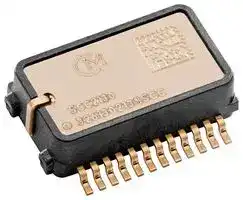


SCA630-EDCV1B
MEMS Accelerometer, Analogue, X, ± 13.3g, 4.75 V, 5.25 V, SMD
- Manufacturer: MURATA
- Product type: MEMS Accelerometers
- No. of Pins: 8Pins
- Sensitivity Typ: 0.15V/g
- Measurement Axis: X
- Sensor Case Style: SMD
- Acceleration Range: ± 13.3g
- MEMS Sensor Output: Analogue
- Supply Voltage Max: 5.25V
- Supply Voltage Min: 4.75V
| Delivery and price | |
|---|---|
| Units per pack | 25 |
| Price | 2.52 € |
| Current stock | 10+ |
| Lead time | 30 days |
**==> picture [84 x 8] intentionally omitted <==**
**----- Start of picture text -----**<br>
SCA630-EDCV1B<br>**----- End of picture text -----**<br>
## **Datasheet**
## **SCA630-EDCV1B SINGLE AXIS ACCELEROMETER WITH ANALOG INTERFACE**
The SCA630 accelerometer consists of a silicon bulk micro machined sensing element chip and a signal conditioning ASIC. The chips are mounted on a pre-molded package and wire bonded to appropriate contacts. The sensing element and ASIC are protected with silicone gel and lid. The sensor has 8 SMD legs (Gull-wing type).
## **Features**
## **Applications**
- Single +5 V supply
- Current consumption 2.5 mA typical
- Ratiometric output in relation to supply voltage (Vdd = 4.75 V...5.25 V)
- Enhanced failure detection features
- Digitally activated, true self-test by proof mass deflection using electrostatic force
- Memory parity check during power up, and self-test cycle.
SCA630 product family is targeted to automotive applications with high stability and reliability requirements. Typical applications include:
- Electronic Stability Control (ESC)
- Engine Vibration Measurement
- Roll Over
- Suspension
- Inclination
- Built in connection failure detection
- Digitally activated, true self-test by proof mass deflection using electrostatic force
- Wide load drive capability (max. 20 nF)
- True DC response
- Qualified according to AEC-Q100 standard
**==> picture [246 x 198] intentionally omitted <==**
**----- Start of picture text -----**<br>
5V supply<br>Measurement Gain &<br>circuitry filtering Vout<br>Sensing<br>element EEPROM for calibration Digital self<br>constants (32 bit, pari ty check)<br>test input<br>ASIC<br>GND 4 programming lines<br>for factory use only<br>|<br>**----- End of picture text -----**<br>
**Figure 1.** Functional block diagram.
Murata Electronics Oy www.muratamems.fi
1/13 Rev.B
Doc.nr. 82 841 00
SCA630-EDCV1B
## **Table of Contents**
|**Table of Contents**|**Table of Contents**|
|---|---|
|SCA630-EDCV1B single axis accelerometer with analog interface ................................... 1||
|FEATURES.................................................................................................................................... 1||
|APPLICATIONS.............................................................................................................................. 1||
|TABLE OF|ABLE OFCONTENTS.................................................................................................................... 2|
|1.|Electrical Specifications ............................................................................................ 3|
|1.1.|ABSOLUTEMAXIMUMRATINGS............................................................................................ 3|
|1.2.|PERFORMANCECHARACTERISTICS..................................................................................... 3|
|1.3.|OFFSET AND SENSITIVITY CALIBRATION................................................................................ 4|
|1.4.|ERROR CALCULATIONS....................................................................................................... 4|
|1.5.|SUPPLY VOLTAGE............................................................................................................... 5|
|1.6.|ELECTRICALCONNECTION.................................................................................................. 6|
|1.7.|LIMITER FUNCTION............................................................................................................. 7|
|1.8.|TYPICALPERFORMANCECHARACHTERISTICS...................................................................... 8|
|2.|Functional Description .............................................................................................. 9|
|2.1.|MEASURING DIRECTIONS.................................................................................................... 9|
|2.2.|VOLTAGE TO ACCELERATION CONVERSION.......................................................................... 9|
|2.3.|RATIOMETRICOUTPUT....................................................................................................... 9|
|2.4.|SELFTEST AND FAILURE DETECTION MODES......................................................................... 9|
|3.|Mechanical Specification ........................................................................................ 11|
|3.1.|DIMENSIONS.................................................................................................................... 11|
|4.|Application information ............................................................................................ 12|
|4.1.|RECOMMENDEDPCBLAY-OUT......................................................................................... 12|
|4.2.|REFLOW SOLDERING........................................................................................................ 13|
Murata Electronics Oy www.muratamems.fi
2/14 Rev.B
Doc. nr. 82 841 00
SCA630-EDCV1B
## **1. Electrical Specifications**
## **1.1. Absolute Maximum Ratings**
|**Parameter **|**Value**|**Units**|
|---|---|---|
|Acceleration(powered or non-powered)|20 000(1|g|
|Supplyvoltage|−0.3 to +7.0|V|
|Voltage at input / output pins|−0.3 to VDD + 0.3|V|
|ESD HBM(Human BodyModel)|2|kV|
|ESD CDM (Charged Device Model)|500 middle pins<br>750 cornerpins|V|
|Temperaturerange (storage)|−50to+125|°C|
|Temperature range(operating)|−40 to +125|°C|
- ~~1~~ Equals to drop from 1 meter on a concrete surface.
## **1.2. Performance Characteristics**
VDD = 5.00 V and ambient temperature unless otherwise specified.
|**KPC**A)|**Parameter **|**Condition **|**Min.**|**Typ**|**Max.**|**Units**|
|---|---|---|---|---|---|---|
||Measuringrange|Nominal|-12.3||+13.3|g|
||Supplyvoltage Vdd||4.75|5.0|5.25|V|
|<CC>|Current consumption|Vdd = 5 V;No load||2.5|4.0|mA|
||Operatingtemperature||−40||+125|°C|
||Resistive output load|Vout to Vdd or Vss|20|||kΩ|
||Capacitive load|Vout to Vdd or Vss|||20|nF|
||Min. output voltage;Vdd = 5 V|20k from Vout to Vdd|0||0.25|V|
||Max. output voltage;Vdd = 5 V|20k from Vout to Vss|4.75||5.00|V|
||Linear output voltage range|Limiter function<br>enabled|0.5||4.5|V|
|<CC>|Offset(Outputat +1g)|@room temperature||Vdd/2||V|
|<CC>|Sensitivity|@ room temperature||0.150<br>(0.03*Vdd)||V/g|
|<SC>|Offset Error(Output at +1g)|−40 °C...125 °C|-870|0|+870|mg|
|<SC>|Sensitivity error|−40°C...125°C|−5|0|+5|%|
||Typical non-linearity<br>~~B)~~|Within the measuring<br>range|−400||+400|mg|
||Amplitude response −3 dB~~B)~~||250|400|550|Hz|
||Ratiometric error|Vdd = 4.75 V...5.25 V|−2||+2|%|
|<SC>|Cross-axis sensitivity|@room temperature|||3.9|%|
||Output noise|From DC...4 kHz|||5|mVrms|
||Start-updelay|Reset andparitycheck|||10|ms|
||Self test pull down resistor<br>(Internal)||44|62|80|kΩ|
1. CC= Critical Characteristics. Must be 100% monitored during production SC= Significant Characteristic. The process capability (Cpk) must be better than 1.33, which allows sample based testing. If process is not capable the part will be 100% tested
2. Output has true DC response
Murata Electronics Oy www.muratamems.fi
3/14 Rev.B
Doc. nr. 82 841 00
SCA630-EDCV1B
## **1.3. Offset and sensitivity calibration**
Vout offset is calibrated in 0g position:
**==> picture [106 x 15] intentionally omitted <==**
Nominal offset is Vdd/2:
**==> picture [92 x 26] intentionally omitted <==**
Sensitivity is calibrated as:
**==> picture [195 x 32] intentionally omitted <==**
Nominal sensitivity is:
_Sensitivitynom_ .0150 [V/g]
## **1.4. Error calculations**
Total error is the allowed maximum error, which include partial error sources. Total error over lifetime is specified as a sum of offset and sensitivity errors:
_Total_ Error_ _Offset_ Error_ _Sensitivity_ Error_ [mg]
Offset error is specified as:
**==> picture [190 x 43] intentionally omitted <==**
Sensitivity error percent is specified as:
**==> picture [362 x 33] intentionally omitted <==**
Sensitivity error is specified as:
_Sensitivity_ Error_ _Vout_ _Vout_ 1 _g_ _Sensitivity_ Error_ % [mg] _Sensitivity_
Murata Electronics Oy www.muratamems.fi
4/14 Rev.B
Doc. nr. 82 841 00
SCA630-EDCV1B
## **1.5. Supply voltage**
Usage of external 100 nF power supply bypass capacitor is recommended.
ASIC start-up should be tolerant to noise between Vdd and GND. Recommended power-up ramp is presented below.
|**Parameter **|**Min**|**Max **|
|---|---|---|
|T1|T0+0.1µs||
|T2||T0+ 100 μs|
|V1|−0.3V|0.5V|
|V2|2.7 V|5.5V|
Supply voltage ramp at startup.
supply voltage
**==> picture [300 x 71] intentionally omitted <==**
**----- Start of picture text -----**<br>
V2<br>V1 t<br>T0 T1 T2<br>**----- End of picture text -----**<br>
**Figure 2.** VDD Start-up sequence.
Murata Electronics Oy www.muratamems.fi
5/14 Rev.B
Doc. nr. 82 841 00
SCA630-EDCV1B
## **1.6. Electrical Connection**
The following is minimum requirement for electrical interface to the SCA630. If over-voltage or reverse polarity protection is needed, please contact VTI Technologies Oy for application information.
Usage of external minimum 100 nF power supply bypass capacitor is recommended. Maximum rise time of VDD is 100 ms.
If self-test (Pin 6) is not used it should be left floating.
Pins 1, 2, 3, and 5 are left floating.
**==> picture [300 x 190] intentionally omitted <==**
**----- Start of picture text -----**<br>
Vdd<br>———©<br>Vout<br>8 7 6 5<br>Hac<br>Min. 100nF<br>SCA630<br>1 2 3 4<br>TI<br>GND<br>**----- End of picture text -----**<br>
**Figure 3.**
Electrical connection of SCA630 component.
|**Pin#**|**Pin Name**|**I/O**|**Function **|**Connection on PCB **|
|---|---|---|---|---|
|1|CLK|||Float/Notconnected|
|2|C1|||Float/Notconnected|
|3|MODE|||Float/Notconnected|
|4|GND|Supply|Negative supply voltage (VSS)|Ground|
|5|PGM|||Float / Not connected|
|6|ST|Input|Self-testcontrol|Float when notused|
|7|VOUT|Output|Sensoroutput voltage|Measuring circuit input|
|8|VDD|Supply|Positive supply voltage (VDD)|Vdd (+5V)|
Murata Electronics Oy www.muratamems.fi
6/14 Rev.B
Doc. nr. 82 841 00
SCA630-EDCV1B
## **1.7. Limiter function**
The table below defines the limiter function.
|**Parameter **|**Condition **|**Min**|**Max **|**Unit**|
|---|---|---|---|---|
|Limiter cutoff voltage|Low voltage limit<br>High voltagelimit|0.05 × Vdd<br>0.90× Vdd|0.10 × Vdd<br>0.95× Vdd|V<br>V|
|Minoutput voltage|Limiterenabled,VDD =5V|0.25||V|
|Max output voltage|Limiter enabled,VDD = 5 V||4.75|V|
|Linear range|Limiterenabled,VDD =5V|0.5|4.5|V|
**==> picture [276 x 227] intentionally omitted <==**
**----- Start of picture text -----**<br>
1.0<br>0.9<br>p | | | EE<br>0.8 p f |] | | tt |e<br>0.7 p f | tt | |<br>Output 0.6<br>p t tT tT | | | a<br>as<br>Ratio 0.5 p f | | | | av<br>to<br>VDD 0.4 p t | | | aA<br>0.3 | | | | ba | tt<br>0.2 p li<br>0.1 | i b a | | || tttttt<br>0.0 |<br>Min Max<br>Acceleration<br>Figure 4. Limiter function.<br>**----- End of picture text -----**<br>
Limiter function limits the output voltage between specified upper and lower limit. In normal operation (VDD = 5.0 V), when limiter is enabled, the output voltage is valid between 0.5 V…4.5 V. Limiting activates between 0.25 V…0.5 V and 4.5 V…4.75 V. Only failures drive output voltage beyond cutoff voltages.
Murata Electronics Oy www.muratamems.fi
7/14 Rev.B
Doc. nr. 82 841 00
SCA630-EDCV1B
## **1.8. Typical Performance Charachteristics**
Typical offset and sensitivity temperature dependencies of the SCA630-EDCV1B are presented in following diagrams. These results represent the typical performance of SCA630-EDCV1B components. The mean value and 3 sigma limits (mean ± 3 standard deviation) and specification limits are presented in following diagrams. The 3 sigma limits represents 99.73% of the SCA630EDCV1B population.
**Figure 5.** Typical temperature dependency of offset at 0g position.
**Figure 6.** Typical temperature dependency of sensitivity.
Murata Electronics Oy www.muratamems.fi
8/14 Rev.B
Doc. nr. 82 841 00
SCA630-EDCV1B
## **2. Functional Description**
## **2.1. Measuring directions**
**==> picture [388 x 142] intentionally omitted <==**
**----- Start of picture text -----**<br>
+ -<br>- +<br>+1 g position 0 g position -1 g position<br>Vout,nom = 2.5 V Vout,nom = 2.35 V Vout,nom = 2.20 V<br>**----- End of picture text -----**<br>
## **2.2. Voltage to acceleration conversion**
Analog output can be transferred to acceleration using the following equation for conversion:
**==> picture [160 x 31] intentionally omitted <==**
where: Vout(0g) = nominal output of the device at 0g position with 5 V supply voltage (ratiometric output), Sensitivity is the sensitivity of the device and Vout is the output of the sensor.
## **2.3. Ratiometric Output**
Ratiometric output means that the zero offset point and sensitivity of the sensor are proportional to the supply voltage. If the SCA6X0 supply voltage is fluctuating the SCA6X0 output will also vary. When the same reference voltage for both the SCA6X0 sensor and the measuring part (A/Dconverter) is used, the error caused by reference voltage variation is automatically compensated for.
## **2.4. Selftest and failure detection modes**
To ensure reliable measurement results the SCA6X0 has continuous interconnection failure and calibration memory validity detection. A detected failure forces the output signal close to power supply ground or VDD level, outside the normal output range.
The calibration memory validity is verified by continuously running parity check for the control register memory content. In the case where a parity error is detected, the control register is automatically re-loaded from the EEPROM. If a new parity error is detected after re-loading data analog output voltage is forced to go close to ground level (<0.25 V).
The SCA6X0 also includes a separate self test mode. The true self test simulates acceleration, or deceleration, using an electrostatic force. The electrostatic force simulates acceleration that is high enough to deflect the proof mass to the extreme positive position, and this causes the output signal to go to the maximum value. The self test function is activated by a separate on-off command on the self test input.
Murata Electronics Oy www.muratamems.fi
9/14 Rev.B
Doc. nr. 82 841 00
SCA630-EDCV1B
The self-test generates an electrostatic force, deflecting the sensing element’s proof mass, thus checking the complete signal path. The true self test performs following checks:
- Sensing element movement check
- ASIC signal path check
- PCB signal path check
- Micro controller A/D and signal path check
The created deflection can be seen in analogue output. Self test can be activated applying logic”1” (positive supply voltage level) to ST pin (pins 6) of SCA6X0. The self test Input high voltage level is 4 – Vdd+0.3 V and input low voltage level is 0.3 – 1 V.
**==> picture [368 x 152] intentionally omitted <==**
**----- Start of picture text -----**<br>
5 V ST pin<br>voltage<br>0 V<br>5V<br>V1 V2 V3<br> Vout<br>T1 T2 T3<br>0 V ——<br>T5 TIME [ MS ] T4<br>**----- End of picture text -----**<br>
**Figure 7.** Self test wave forms.
V1 = initial output voltage before the self test function is activated. V2 = output voltage during the self test function.
V3 = output voltage after the self test function has been de-activated and after stabilization time Please note that the error band specified for V3 is to guarantee that the output is within 5% of the initial value after the specified stabilization time. After a longer time (max. 1 second) V1=V3. T1 = Pulse length for Self test activation
T2 = Saturation delay
T3 = Recovery time
T4 = Stabilization time =T2+T3
T5 = Rise time during self test.
|T1[ms]|T2[ms]|T3 [ms]|T4[ms]|T5 [ms]|V2:|V3:|
|---|---|---|---|---|---|---|
|10-100|Typ. 20|Typ. 50|Typ. 70|Typ. 10|Typical min.<br>0.54*VDD (2.7 V<br>@Vdd=5V)|0.95*V1-<br>1.05*V1|
Self test characteristics.
Murata Electronics Oy www.muratamems.fi
10/14 Rev.B
Doc. nr. 82 841 00
SCA630-EDCV1B
## **3. Mechanical Specification**
Lead frame material: Copper Plating: Nickel followed by Gold Solderability: JEDEC standard: JESD22-B102-C Co-planarity: 0.1 mm max. The part weights: ~0.73 g
## **3.1. Dimensions**
**Figure 8.** Mechanical dimensions [mm].
Murata Electronics Oy www.muratamems.fi
11/14 Rev.B
Doc. nr. 82 841 00
SCA630-EDCV1B
## **4. Application information**
The SCA6X0 should be powered from a well regulated 5 V DC power supply. Coupling of digital noise to the power supply line should be minimized. 100nF filtering capacitor between VDD pin 8 and GND plane must be used. If regulator is placed far from component for example other PCB it is recommend adding more capacitance between VDD and GND to ensure current drive capability of the system. For example 470 pF and 1uF capacitor can be used.
The SCA6X0 has a ratiometric output. To get the best performance use the same reference voltage for both the SCA6X0 and Analog/Digital converter.
Locate the 100nF power supply filtering capacitor close to VDD pin 8. Use as short a trace length as possible. Connect the other end of capacitor directly to the ground plane. Connect the GND pin 4 to underlying ground plane. Use as wide ground and power supply planes as possible. Avoid narrow power supply or GND connection strips on PCB.
## **4.1. Recommended PCB lay-out**
**Figure 9.** Recommended PCB lay-out [mm].
## **Notes:**
- It is important that the part is parallel to the PCB plane and that there is no angular alignment error from intended measuring direction during assembly process.
- 1° mounting alignment error will increase the cross-axis sensitivity by 1.7%
- 1° mounting alignment error will change the output by 17 mg
- Wave soldering is not recommended
- Ultrasonic cleaning is not allowed
- A supply voltage by-pass capacitor (> 100 nF) is recommended
Murata Electronics Oy www.muratamems.fi
12/14 Rev.B
Doc. nr. 82 841 00
SCA630-EDCV1B
## **4.2. Reflow soldering**
The SCA6X0 is suitable for Sn-Pb eutectic and Pb- free soldering process and mounting with normal SMD pick-and-place equipment. Recommended body temperature profile during reflow soldering:
**Figure 10.** Recommended body temperature profile during reflow soldering. Ref. IPC/JEDEC J-STD-020D.
|**Profile feature**|**Sn-Pb Eutectic**<br>**Assembly**|**Pb-free Assembly**|
|---|---|---|
|Average ramp-uprate(TLto TP)|3 °C/second max.|3 °C/second max.|
|Preheat<br>-<br>Temperature min (Tsmin)<br>-<br>Temperature max (Tsmax)<br>-<br>Time(min to max) (ts)|100 °C<br>150 °C<br>60-120 seconds|150 °C<br>200 °C<br>60-180 seconds|
|Tsmax to TL<br>- Rampuprate||3°C/second max|
|Time maintained above:<br>-<br>Temperature (TL)<br>-<br>Time(tL)|183 °C<br>60-150 seconds|217 °C<br>60-150 seconds|
|Peak temperature(TP)|240 +0/−5 °C|250 +0/−5 °C|
|Time within 5 °C of actual Peak Temperature<br>(TP)|10-30 seconds|20-40 seconds|
|Ramp-down rate|6 °C/second max|6 °C/second max|
|Time 25 °C to Peak temperature|6 minutes max|8 minutes max|
The Moisture Sensitivity Level of the part is 3 according to the IPC/JEDEC J-STD-020D. The part should be delivered in a dry pack. The manufacturing floor time (out of bag) in the customer’s end is 168 hours.
Murata Electronics Oy www.muratamems.fi
13/14 Rev.B
Doc. nr. 82 841 00
SCA630-EDCV1B
## **Notes:**
- Preheating time and temperatures according to guidance from solder paste manufacturer.
- It is important that the part is parallel to the PCB plane and that there is no angular alignment error from intended measuring direction during assembly process.
- Wave soldering is not recommended.
- **Ultrasonic cleaning is not allowed** . The sensing element may be damaged by an ultrasonic cleaning process
The Moisture Sensitivity Level of the part is 3 according to the IPC/JEDEC J-STD020B. The part should be delivered in a dry pack. The manufacturing floor time (out of bag) in the customer’s end is 168 hours. Maximum soldering temperature is 250 °C/40 sec.
Rework after the initial soldering process is not recommended. Rework can cause heat build-up to the leg and this heat build-up will cause the housing material to get soft thus allowing the leg to move. The movement can cause bond wire disconnection inside the part.
Murata Electronics Oy www.muratamems.fi
14/14 Rev.B
Doc. nr. 82 841 00
Updated at February 9, 2023
Established in Kyoto in 1944, Murata has grown into a global leader in the design and manufacture of advanced electronic components, specializing in ceramic passive components, wireless connectivity modules, and power conversion technologies. Renowned for its foundational work in materials science and process innovation, Murata delivers solutions that drive the evolution of modern electronics across telecommunications, mobility, industrial, and healthcare applications. This extensive portfolio is anchored by a broad selection of high-performance passive components, heavily focused on inductive solutions. Engineers can choose from hundreds of specialized RF inductors and power inductors engineered for exceptional reliability, efficiency, and miniaturization. The range also features robust EMC and RFI suppression solutions, highlighted by industry-leading common mode chokes and power line filters designed to ensure signal integrity and strict regulatory compliance in demanding circuit environments. Beyond inductive and filtering components, the offering encompasses a comprehensive array of critical circuit protection, timing, and power devices. Murata's precision NTC and PTC thermistors provide essential temperature sensing and thermal management, while its robust lineup of ceramic resonators and quartz crystals ensures highly accurate frequency control. Supported by premium non-rechargeable batteries, polymer capacitors, and advanced sensing transducers, Murata equips designers with the versatile building blocks required for next-generation technological development.
About Novapart
Novapart is a B2B electronic component broker specialising in stock shortages and cost reduction. We source hard-to-find parts and identify compliant alternatives across a catalogue of 410,000+ components from 500+ manufacturers.
Learn more →Stock Shortage Specialist
When a component is unavailable, discontinued or has an unacceptable lead time, we tap into our network of vetted European and Asian distributors to source what you need — without compromising on quality or traceability.
Request a quote →Compliant Alternatives
We identify pin-to-pin, electrically equivalent substitutes that meet the same certifications (RoHS, AEC-Q100, REACH) as your original specification — validated against datasheets, not just part numbers. Often at a lower cost.
BOM Analysis service →