


SBRB1545CTT4G
Schottky Rectifier, 45 V, 15 A, Dual Common Cathode, TO-263 (D2PAK), 3 Pins, 840 mV
- Manufacturer: ONSEMI
- Product type: Schottky Rectifier Diodes
- SVHC: No SVHC (25-Jun-2025)
- No. of Pins: 3Pins
- Product Range: -
- Qualification: AEC-Q101
- Diode Mounting: Surface Mount
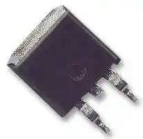
- Diode Case Style: TO-263 (D2PAK)
- Diode Configuration: Dual Common Cathode
- Forward Voltage Max: 840mV
- Forward Surge Current: 150A
- Average Forward Current: 15A
- Operating Temperature Max: 175°C
- Repetitive Peak Reverse Voltage: 45V
| Delivery and price | |
|---|---|
| Units per pack | 800 |
| Price | 0.462 € |
| Current stock | 10+ |
| Lead time | 30 days |
**Share Feedback DATA SHEET** Your Opinion Matters **www.onsemi.com** ~~oe~~
## Switch-mode Power Rectifier
## D[2] PAK Surface Mount Power Package
## **SCHOTTKY BARRIER RECTIFIER 15 AMPERES 45 VOLTS**
## MBRB1545CTG, SBRB1545CTG
**==> picture [192 x 168] intentionally omitted <==**
**----- Start of picture text -----**<br>
D [2] PAK<br>CASE 418B<br>STYLE 3<br>1<br>4<br>3<br>a<br>MARKING DIAGRAM<br>AY WW<br>B1545G<br> AKA<br>**----- End of picture text -----**<br>
The D[2] PAK Power Rectifier employs the Schottky Barrier principle **CASE 418B** with a platinum barrier metal. These state-of-the-art devices have the **STYLE 3** following features:
**Features** 1 Center−Tap Configuration 4 3
- Guardring for Stress Protection
- Low Forward Voltage
- 175 C Operating Junction Temperature
- Epoxy Meets UL 94, V−0 @ 0.125 in
- Short Heatsink Tab Manufactured − Not Sheared
- Similar in Size to the Industry Standard TO220 Package
- SBRB Prefix for Automotive and Other Applications Requiring Unique Site and Control Change Requirements; AEC−Q101 Qualified and PPAP Capable
- These Devices are Pb−Free and are RoHS Compliant*
## **Mechanical Characteristics**
- Case: Epoxy, Molded, Epoxy Meets UL 94, V−0
- Weight: 1.7 grams (approximately)
- Finish: All External Surfaces Corrosion Resistant and Terminal Leads are Readily Solderable
- Lead and Mounting Surface Temperature for Soldering Purposes: 260 C Max. for 10 Seconds
- Device Meets MSL1 Requirements
- ESD Ratings:
- Machine Model = C (> 400 V)
**==> picture [106 x 58] intentionally omitted <==**
**----- Start of picture text -----**<br>
B1545 = Device Code<br>A = Assembly Location<br>Y = Year<br>WW = Work Week<br>G = Pb−Free Package<br>AKA = Diode Polarity<br>**----- End of picture text -----**<br>
## **ORDERING INFORMATION**
See detailed ordering and shipping information on page 3 of this data sheet.
NOTE: Some of the devices on this data sheet have been **DISCONTINUED** . Please refer to the table on page 3.
- Human Body Model = 3B (> 8000 V)
> *For additional information on our Pb-Free strategy and soldering details, please download the **onsemi** Soldering and Mounting Techniques Reference Manual, SOLDERRM/D.
Publication Order Number: **MBRB1545CT/D**
**1**
Semiconductor Components Industries, LLC, 2012 **November, 2024 − Rev. 14**
**MBRB1545CTG, SBRB1545CTG**
## **MAXIMUM RATINGS** (Per Leg)
|**Symbol**|**Rating**|**Value**|**Unit**|
|---|---|---|---|
|VRRM<br>VRWM<br>VR|Peak Repetitive Reverse Voltage<br>Working Peak Reverse Voltage<br>DC Blocking Voltage|45|V|
|IF(AV)|Average Rectified Forward Current<br>(Rated VR, TC= 167C) Total Device|7.5<br>15|A|
|IFRM|Peak Repetitive Forward Current<br>(Rated VR, Square Wave, 20 kHz, TC= 166C)|15|A|
|IFSM|Non−Repetitive Peak Surge Current<br>(Surge Applied at Rated Load Conditions Halfwave, Single Phase, 60 Hz)|150|A|
|IRRM<br>~~a~~|Peak Repetitive Reverse Surge Current (2.0 s, 1.0 kHz)|1.0|A|
|Tstg|Storage Temperature Range|−65 to +175|C|
|TJ|Operating Junction Temperature (Note 1)|−65 to +175|C|
|dv/dt<br>~~a~~|Voltage Rate of Change (Rated VR)|10,000|V/ s|
Stresses exceeding those listed in the Maximum Ratings table may damage the device. If any of these limits are exceeded, device functionality should not be assumed, damage may occur and reliability may be affected.
1. The heat generated must be less than the thermal conductivity from Junction−to−Ambient: dPD/dTJ < 1/R 8 JA.
## **THERMAL CHARACTERISTICS** (Per Leg)
|**Symbol**|**Characteristic**|**Value**|**Unit**|
|---|---|---|---|
|R JC<br>R JA<br>8<br>8|Thermal Resistance<br>Junction to Case<br>Junction to Ambient (Note 2)|2.0<br>50|C/W|
2. When mounted using minimum recommended pad size on FR−4 board.
## **ELECTRICAL CHARACTERISTICS** (Per Leg)
|**ELECTRICAL CHARACTERISTICS**|**ELECTRICAL CHARACTERISTICS**(Per Leg)|||
|---|---|---|---|
|**Symbol**|**Characteristic**|**Value**|**Unit**|
|VF|Maximum Instantaneous Forward Voltage (Note 3)<br>(iF= 7.5 Amps, TJ= 125C)<br>(iF= 15 Amps, TJ= 125C)<br>(iF= 15 Amps, TJ= 25C)|0.57<br>0.72<br>0.84|V|
|iR|Maximum Instantaneous Reverse Current (Note 3)<br>(Rated dc Voltage, TJ= 125C)<br>(Rated dc Voltage, TJ= 25C)|15<br>0.1|mA|
3. Pulse Test: Pulse Width = 300 s, Duty Cycle u 2.0%.
**www.onsemi.com**
**Share Feedback** Your Opinion Matters
**2**
**MBRB1545CTG, SBRB1545CTG**
## **TYPICAL CHARACTERISTICS**
**==> picture [489 x 408] intentionally omitted <==**
**----- Start of picture text -----**<br>
50<br>SSS SSSS S SSS<br>3020 OEE 10 a a a a a<br>10 125 C<br>aes eee 1 ee<br>3 85 C<br>2 Se ee Se —— eee<br>1 DO 0.1<br>0.5 125 C 85 C 25 C 0.01 25 C<br>i oo oo eee eeE e<br>-—__{ | __+__{___}___}__}__ J e e<br>Ps es ss 0.001 | +r | [| {| { { { { {|<br>0.1 0.2 0.3 0.4 0.5 0.6 0.7 0.8 0.9 0 10 20 30 40 50<br>vF, INSTANTANEOUS FORWARD VOLTAGE (VOLTS) VR, REVERSE VOLTAGE (VOLTS)<br>Figure 1. Typical Forward Voltage, Per Leg Figure 2. Typical Reverse Current, Per Leg<br>14<br>16<br>TJ = 125 C IPK = DC<br>14 Pe I AV 12<br>IPK<br>12 pf | IPK = 10 IAV = 5 i 10 e e<br>10 IPK I AV SQUARE<br>= = 20 oA 8 V N<br>IAV<br>8 + p68<br>DC 6<br>6<br>| Spe 4 f o<br>| SQUARE S<br>4<br>WAVE<br>2<br>2 OB B AP eeee\<br>0 Ae FF] hE 0 dTUN<br>0 2 4 6 8 10 12 14 16 155 160 165 170 175<br>IF(AV), AVERAGE FORWARD CURRENT (AMPS) TC, CASE TEMPERATURE (C)<br>, REVERSE LEAKAGE CURRENT (mA)<br>IR<br>iF, INSTANTANEOUS FORWARD CURRENT (AMPS)<br>, AVERAGE FORWARD CURRENT (A)<br>, AVERAGE FORWARD POWER DISSIPATION (WATTS)PF(AV) IF(AV)<br>**----- End of picture text -----**<br>
**Figure 3. Typical Forward Power Dissipation**
**Figure 4. Current Derating, Case, Per Leg**
## **ORDERING INFORMATION**
|**ORDERING INFORMATION**|||
|---|---|---|
|**Device**|**Package**|**Shipping**†|
|MBRB1545CTT4G|D2PAK<br>(Pb−Free)|800 / Tape & Reel|
|SBRB1545CTT4G|D2PAK<br>(Pb−Free)|800 / Tape & Reel|
## **DISCONTINUED** (Note 4)
|**DISCONTINUED**(Note 4)|||
|---|---|---|
|MBRB1545CTG|D2PAK<br>(Pb−Free)|50 Units / Rail|
|SBRB1545CTG|D2PAK<br>(Pb−Free)|50 Units / Rail|
†For information on tape and reel specifications, including part orientation and tape sizes, please refer to our Tape and Reel Packaging Specifications Brochure, BRD8011/D.
4. **DISCONTINUED:** These devices are not recommended for new design. Please contact your **onsemi** representative for information. The most current information on these devices may be available on www.onsemi.com.
**www.onsemi.com 3** ~~—~~
**Share Feedback** Your Opinion Matters
MECHANICAL CASE OUTLINE **PACKAGE DIMENSIONS**
**D[2] PAK 3** CASE 418B−04 ISSUE L
**==> picture [56 x 45] intentionally omitted <==**
DATE 17 FEB 2015
**SCALE 1:1**
**==> picture [441 x 418] intentionally omitted <==**
**----- Start of picture text -----**<br>
NOTES:<br>C 1. DIMENSIONING AND TOLERANCING<br>PER ANSI Y14.5M, 1982.<br>E 2. CONTROLLING DIMENSION: INCH.<br>−B− V 3. 418B−01 THRU 418B−03 OBSOLETE,NEW STANDARD 418B−04.<br>W<br>4 INCHES MILLIMETERS<br>DIM MIN MAX MIN MAX<br>A 0.340 0.380 8.64 9.65<br>B 0.380 0.405 9.65 10.29<br>A C 0.160 0.190 4.06 4.83<br>S D 0.020 0.035 0.51 0.89<br>1 2 3 E 0.045 0.055 1.14 1.40<br>F 0.310 0.350 7.87 8.89<br>G 0.100 BSC 2.54 BSC<br>−T− H 0.080 0.110 2.03 2.79<br>K J 0.018 0.025 0.46 0.64<br>SEATINGPLANE G J W KL 0.0900.052 0.0720.110 2.291.32 2.791.83<br>M 0.280 0.320 7.11 8.13<br>H N 0.197 REF 5.00 REF<br>D 3 PL P 0.079 REF 2.00 REF<br>R 0.039 REF 0.99 REF<br>0.13 (0.005) M T B M S 0.575 0.625 14.60 15.88<br>V 0.045 0.055 1.14 1.40<br>VARIABLE<br>CONFIGURATION<br>ZONE N P<br>R<br>U<br>L L L<br>M M M<br>F F F<br>VIEW W−W VIEW W−W VIEW W−W<br>1 2 3<br>STYLE 1: STYLE 2: STYLE 3: STYLE 4: STYLE 5: STYLE 6:<br>PIN 1. BASE PIN 1. GATE PIN 1. ANODE PIN 1. GATE PIN 1. CATHODE PIN 1. NO CONNECT<br>2. COLLECTOR 2. DRAIN 2. CATHODE 2. COLLECTOR 2. ANODE 2. CATHODE<br>3. EMITTER 3. SOURCE 3. ANODE 3. EMITTER 3. CATHODE 3. ANODE<br>4. COLLECTOR 4. DRAIN 4. CATHODE 4. COLLECTOR 4. ANODE 4. CATHODE<br>**----- End of picture text -----**<br>
## **MARKING INFORMATION AND FOOTPRINT ON PAGE 2**
**==> picture [493 x 37] intentionally omitted <==**
**----- Start of picture text -----**<br>
Electronic versions are uncontrolled except when accessed directly from the Document Repository.<br>DOCUMENT NUMBER: 98ASB42761B Printed versions are uncontrolled except when stamped “CONTROLLED COPY” in red.<br>DESCRIPTION: D [2] PAK 3 PAGE 1 OF 2<br>**----- End of picture text -----**<br>
**onsemi** and are trademarks of Semiconductor Components Industries, LLC dba **onsemi** or its subsidiaries in the United States and/or other countries. **onsemi** reserves the right to make changes without further notice to any products herein. **onsemi** makes no warranty, representation or guarantee regarding the suitability of its products for any particular purpose, nor does **onsemi** assume any liability arising out of the application or use of any product or circuit, and specifically disclaims any and all liability, including without limitation special, consequential or incidental damages. **onsemi** does not convey any license under its patent rights nor the rights of others.
www.onsemi.com
© Semiconductor Components Industries, LLC, 2019
DATE 17 FEB 2015
**==> picture [64 x 30] intentionally omitted <==**
**----- Start of picture text -----**<br>
D [2] PAK 3<br>CASE 418B−04<br>ISSUE L<br>**----- End of picture text -----**<br>
**==> picture [182 x 193] intentionally omitted <==**
**----- Start of picture text -----**<br>
GENERIC<br>MARKING DIAGRAM*<br>xx AYWW<br>xxxxxxxxG<br>xxxxxxxxx xxxxxxxxG<br>AYWW<br>AWLYWWG AKA<br>IC Standard Rectifier<br>xx = Specific Device Code<br>A = Assembly Location<br>WL = Wafer Lot<br>Y = Year<br>WW = Work Week<br>G = Pb−Free Package<br>AKA = Polarity Indicator<br>**----- End of picture text -----**<br>
*This information is generic. Please refer to device data sheet for actual part marking. Pb−Free indicator, “G” or microdot “ � ”, may or may not be present. Some products may not follow the Generic Marking.
## **SOLDERING FOOTPRINT***
**==> picture [147 x 173] intentionally omitted <==**
**----- Start of picture text -----**<br>
10.49<br>8.38<br>16.155<br>2X<br>3.504<br>2X<br>1.016<br>5.080<br>PITCH<br>DIMENSIONS: MILLIMETERS<br>**----- End of picture text -----**<br>
*For additional information on our Pb−Free strategy and soldering details, please download the **onsemi** Soldering and Mounting Techniques Reference Manual, SOLDERRM/D.
Electronic versions are uncontrolled except when accessed directly from the Document Repository. **DOCUMENT NUMBER: 98ASB42761B** Printed versions are uncontrolled except when stamped “CONTROLLED COPY” in red. **DESCRIPTION: D[2] PAK 3 PAGE 2 OF 2**
**onsemi** and are trademarks of Semiconductor Components Industries, LLC dba **onsemi** or its subsidiaries in the United States and/or other countries. **onsemi** reserves the right to make changes without further notice to any products herein. **onsemi** makes no warranty, representation or guarantee regarding the suitability of its products for any particular purpose, nor does **onsemi** assume any liability arising out of the application or use of any product or circuit, and specifically disclaims any and all liability, including without limitation special, consequential or incidental damages. **onsemi** does not convey any license under its patent rights nor the rights of others.
**www.onsemi.com**
~~**2**~~
www.onsemi.com
© Semiconductor Components Industries, LLC, 2019
**onsemi** , , and other names, marks, and brands are registered and/or common law trademarks of Semiconductor Components Industries, LLC dba “ **onsemi** ” or its affiliates and/or subsidiaries in the United States and/or other countries. **onsemi** owns the rights to a number of patents, trademarks, copyrights, trade secrets, and other intellectual property. A listing of **onsemi** ’s product/patent coverage may be accessed at www.onsemi.com/site/pdf/Patent−Marking.pdf. **onsemi** reserves the right to make changes at any time to any products or information herein, without notice. The information herein is provided “as−is” and **onsemi** makes no warranty, representation or guarantee regarding the accuracy of the information, product features, availability, functionality, or suitability of its products for any particular purpose, nor does **onsemi** assume any liability arising out of the application or use of any product or circuit, and specifically disclaims any and all liability, including without limitation special, consequential or incidental damages. Buyer is responsible for its products and applications using **onsemi** products, including compliance with all laws, regulations and safety requirements or standards, regardless of any support or applications information provided by **onsemi** . “Typical” parameters which may be provided in **onsemi** data sheets and/or specifications can and do vary in different applications and actual performance may vary over time. All operating parameters, including “Typicals” must be validated for each customer application by customer’s technical experts. **onsemi** does not convey any license under any of its intellectual property rights nor the rights of others. **onsemi** products are not designed, intended, or authorized for use as a critical component in life support systems or any FDA Class 3 medical devices or medical devices with a same or similar classification in a foreign jurisdiction or any devices intended for implantation in the human body. Should Buyer purchase or use **onsemi** products for any such unintended or unauthorized application, Buyer shall indemnify and hold **onsemi** and its officers, employees, subsidiaries, affiliates, and distributors harmless against all claims, costs, damages, and expenses, and reasonable attorney fees arising out of, directly or indirectly, any claim of personal injury or death associated with such unintended or unauthorized use, even if such claim alleges that **onsemi** was negligent regarding the design or manufacture of the part. **onsemi** is an Equal Opportunity/Affirmative Action Employer. This literature is subject to all applicable copyright laws and is not for resale in any manner.
## **ADDITIONAL INFORMATION**
**TECHNICAL PUBLICATIONS** : **ONLINE SUPPORT** : www.onsemi.com/support **Technical Library:** www.onsemi.com/design/resources/technical−documentation **For additional information, please contact your local Sales Representative at onsemi Website:** www.onsemi.com www.onsemi.com/support/sales
**==> picture [232 x 43] intentionally omitted <==**
Updated at June 4, 2026
onsemi is a premier global supplier of intelligent power and sensing technologies, driving disruptive innovations across the automotive, industrial, and cloud infrastructure markets. Recognized for their commitment to sustainability and reliable supply chains, the company accelerates advancements in vehicle electrification, industrial automation, and 5G networks by solving the industry's most complex design challenges. At the core of their portfolio is an industry-leading selection of discrete semiconductors. This extensive range features thousands of high-performance bipolar transistors, single and dual MOSFETs, and a comprehensive array of diodes, including Zener, Schottky, and fast-recovery rectifiers. Engineered for superior thermal performance and energy efficiency, these foundational components are critical for demanding power conversion, switching, and signal conditioning applications. Beyond essential discretes, onsemi provides a robust suite of advanced power management and circuit protection solutions. Their lineup includes intelligent power modules, single IGBTs, and transient voltage suppression (TVS) diodes designed to safeguard sensitive circuitry. Complimented by integrated passive filters, AC/DC LED driver ICs, and specialized sub-2.4GHz RF transceivers, onsemi equips engineers with the scalable, high-quality technologies needed to build a cleaner, smarter, and more connected world.
About Novapart
Novapart is a B2B electronic component broker specialising in stock shortages and cost reduction. We source hard-to-find parts and identify compliant alternatives across a catalogue of 540,000+ components from 500+ manufacturers.
Learn more →Stock Shortage Specialist
When a component is unavailable, discontinued or has an unacceptable lead time, we tap into our network of vetted European and Asian distributors to source what you need — without compromising on quality or traceability.
Request a quote →Compliant Alternatives
We identify pin-to-pin, electrically equivalent substitutes that meet the same certifications (RoHS, AEC-Q100, REACH) as your original specification — validated against datasheets, not just part numbers. Often at a lower cost.
BOM Analysis service →