
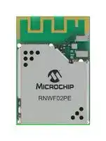


RNWF02PE-I/100
Wi-Fi Module, with PCB Antenna, ADC, DAC, GPIO, I2C, PTA, UART, 2.4 GHz, 2 MB Flash
- Manufacturer: MICROCHIP
- Product type:
- SVHC: No SVHC (04-Feb-2026)
- Frequency RF: 2.4GHz
- Product Range: RNWF02 Series
- Module Interface: ADC, DAC, GPIO, I2C, PTA, UART
- Module Applications: Smart Factories/CCTV/Lighting/Smart Locks/Computing/Wi-Fi Dongles/Prtcl Bridging/IoT/Remote Control
| Delivery and price | |
|---|---|
| Units per pack | 490 |
| Price | 3.11 € |
| Current stock | 100+ |
| Lead time | 30 days |
## **RNWF02 Wi-Fi[®] Module Data Sheet RNWF02**
## **Introduction**
The RNWF02 Module is a low power 2.4 GHz IEEE[®] 802.11b/g/n compliant, fully RF certified wireless module designed for IoT (Internet of Things) applications. These modules are interfaced via a two-wire or four-wire UART interface with Microchip’s simple ASCII-based AT commands for easy integration into most of the applications. The host microcontroller can dynamically configure the RNWF02 module with a few simple ASCII commands.
The Module operates at a single supply voltage VDD (3.3V typical), certain Input Output (IOs) pins support a voltage range of 1.8-3.6V by supplying the VDDIO pin separately.
The RNWF02 module is available with an on-board Printed Circuit Board (PCB) antenna or U.FL connector for an external antenna and with or without Trust&Go CryptoAuthentication[™] device.
## **Features**
- Compliant with IEEE[®] 802.11 b/g/n Single Spatial Stream of 20 MHz Channel Bandwidth
- Transmission Control Protocol/Internet Protocol (TCP/IP)-Based Connectivity Protocols Along with SSL and MQTT Capabilities
- Supports STA Mode and Soft AP Functionality in IEEE 802.11 Infrastructure and IBSS Networks
- Protected Management Frame (PMF) Handled in Hardware, WPA3 Support
- Integrated Power Amplifier (PA) and TX/RX Switch and Power Management
- Internal Flash Memory to Store Firmware
- Immutable Secure Boot with Hardware Root of Trust
- Supports Host Assisted Over-the-Air (OTA) Firmware Update
- On-Chip Network Stack to Offload MCU[(1)]
- Network features – TCP, UDP, DHCP, ARP, HTTP, MQTT, IPv6 TLS 1.2 and DNS
- Hardware accelerators for Wi-Fi[®] and TLS security to improve connection time
- Optional low-power secondary oscillator (RTCC oscillator) 32.768 KHz for real-time clock and calendar applications[(1)(2)]
- Hardware-Based IEEE 802.15.2 Compliant Three-Wire Packet Traffic Arbitration (PTA) Interface for Wi-Fi/ Bluetooth[®] Coexistence[(1)(2)]
- UART Host Interface
- Secure Device Firmware Upgrade (DFU)
- Integrated Trust&Go CryptoAuthentication[™] Device (Optional)
## **Security**
- Hardware Accelerated Security Modes (CryptoMaster) with Built-in DMA Support
- Encryption engines (AES and TDES with different NIST modes of operation):
- Modes – Electronic Code Book (ECB), Cypher Block Chaining (CBC), Counter Mode (CTR), Cypher Feedback Mode (CFB) and Output Feedback Mode (OFB)
Preliminary Data Sheet
DS70005544B - 1
© 2023-2024 Microchip Technology Inc. and its subsidiaries
**RNWF02**
- AES key sizes: 128b, 192b and 256b
- Authentication engines:
- SHA-1 and SHA-2
- AES GCM (Galois/Counter mode)
- HMAC and AES CMAC
- On-chip oscillator for NDRNG generation
- Multi-Purpose Public Key Crypto Engine Supporting the Following Algorithms:
- ECC/ECDH/ECDSA with standard NIST prime curves up to 521-bit, Curve25519 and Ed25519
- RSA up to 2048-bit keys
## **Operating Conditions**
- Operating Voltage (VDD): 3.0-3.6V (3.3V Typical), (VDDIO): 1.8-3.6V
- Operating Temperature: -40°C to 85°C
## **Module Variants**
- PCB Antenna:
- RNWF02PE
- RNWF02PC
- U.FL Connector for External Antenna: – RNWF02UE
- RNWF02UC
## **Package**
- 28-Pin SMD Package with Shield CAN
- Size: 21.7 mm x 14.7 mm x 2.1 mm
## **Applications**
- Smart Factories/Control Devices
- Security Systems, CCTV
- Smart Homes/Lighting, Smart Locks
- Computing, Wi-Fi Dongles, Protocol Bridging
- Internet of Things (IoT) Sensor Tag
- Remote Control
- Wearable Smart Devices
- Industrial Control
## **Certifications**
- RNWF02 Module is Certified to FCC, ISED, UKCA and CE Radio Regulations
- RoHS and REACH Compliant
## **Notes:**
1. Refer to the RNWF02 Application Developer's Guide for the latest supported features.
2. Either the PTA functionality or the RTCC oscillator can be used. Refer to Pin Details of RNWF02 Module for more details.
Preliminary Data Sheet © 2023-2024 Microchip Technology Inc. and its subsidiaries
DS70005544B - 2
**RNWF02**
## **Table of Contents**
|**Table of Contents**|**Table of Contents**|
|---|---|
|Introduction...........................................................................................................................................................................1||
|Features................................................................................................................................................................................. 1||
|1.|Module Ordering Information..................................................................................................................................... 4|
|2.|Device Overview............................................................................................................................................................ 5|
||2.1.<br>Pin Details of RNWF02 Module.........................................................................................................................6|
||2.2.<br>Basic Connection Requirement........................................................................................................................9|
||2.3.<br>RNWF02 Module Placement Guidelines....................................................................................................... 11|
||2.4.<br>RNWF02 Module Routing Guidelines............................................................................................................ 13|
||2.5.<br>RNWF02 Module RF Considerations..............................................................................................................14|
||2.6.<br>RNWF02 Module Antenna Considerations................................................................................................... 14|
||2.7.<br>RNWF02 Module Refow Profle Information............................................................................................... 20|
||2.8.<br>RNWF02 Module Assembly Considerations................................................................................................. 21|
|3.|Electrical Specifcations.............................................................................................................................................. 22|
||3.1.<br>RNWF02 Module Absolute Maximum Ratings............................................................................................. 22|
||3.2.<br>Thermal Specifcations.................................................................................................................................... 22|
||3.3.<br>RNWF02 Module DC Characteristics..............................................................................................................23|
||3.4.<br>RNWF02 Module AC Characteristics..............................................................................................................24|
||3.5.<br>RNWF02 Module Radio Specifcations...........................................................................................................24|
|4.|RNWF02 Module Packaging Information................................................................................................................. 33|
||4.1.<br>RNWF02 Module Packaging Marking.............................................................................................................33|
||4.2.<br>RNWF02 Module Packaging Dimension........................................................................................................33|
|5.|Appendix A: Regulatory Approval............................................................................................................................. 37|
||5.1.<br>United States.................................................................................................................................................... 37|
||5.2.<br>Canada.............................................................................................................................................................. 39|
||5.3.<br>Europe...............................................................................................................................................................41|
||5.4.<br>UKCA (UK Conformity Assessed)....................................................................................................................42|
||5.5.<br>Other Regulatory Information........................................................................................................................43|
|6.|Appendix B: Acronyms and Abbreviations...............................................................................................................44|
|7.|Document Revision History....................................................................................................................................... 46|
|Microchip Information....................................................................................................................................................... 49||
||The Microchip Website............................................................................................................................................... 49|
||Product Change Notifcation Service........................................................................................................................ 49|
||Customer Support.......................................................................................................................................................49|
||Microchip Devices Code Protection Feature............................................................................................................49|
||Legal Notice..................................................................................................................................................................49|
||Trademarks..................................................................................................................................................................50|
||Quality Management System.....................................................................................................................................51|
||Worldwide Sales and Service..................................................................................................................................... 52|
Preliminary Data Sheet
DS70005544B - 3
© 2023-2024 Microchip Technology Inc. and its subsidiaries
**RNWF02 Module Ordering Information**
## **1. Module Ordering Information**
This chapter provides the ordering information of the RNWF02 module.
**Table 1-1.** RNWF02 Module Ordering Details
|Module Name|Description|Regulatory Certifcation|Ordering Code|
|---|---|---|---|
|RNWF02PE|RNWF02 Module with PCB antenna|FCC, ISED, CE, UKCA|RNWF02PE-I/XXX|
|RNWF02PC|RNWF02 Module with PCB antenna and Trust&Go|FCC, ISED, CE, UKCA|RNWF02PC-I/XXX|
|RNWF02UE|RNWF02 Module with U.FL connector for external<br>antenna|FCC, ISED, CE, UKCA|RNWF02UE-I/XXX|
|RNWF02UC|RNWF02 Module with U.FL connector for external<br>antenna and Trust&Go|FCC, ISED, CE, UKCA|RNWF02UC-I/XXX|
The following figure illustrates the details of the RNWF02 module ordering information.
**Figure 1-1.** RNWF02 Module Ordering Information
**==> picture [421 x 233] intentionally omitted <==**
**----- Start of picture text -----**<br>
RN WF 02 P/U E/C T -I /XXX<br> ASCII Command based RN Variant<br>Wi-Fi [®]<br>Flash Memory Size<br>02 = 2 MB Flash<br>Antenna<br>P – PCB Antenna<br>U – U.FL Connector<br>Encryption<br>E - No Encryption<br>C - Trust&Go<br>Packing(1)<br>T = Tape & Reel<br>Temperature<br>Industrial: -40°C to +85°C<br> Firmware Version<br>**----- End of picture text -----**<br>
**Note:** By default, the WINCS02 module comes with Tray packing.
Preliminary Data Sheet © 2023-2024 Microchip Technology Inc. and its subsidiaries
DS70005544B - 4
**RNWF02 Device Overview**
## **2. Device Overview**
The RNWF02 module is a fully RF certified wireless module. The RNWF02 module is available with the following antenna variants:
- PCB antenna (RNWF02PE/RNWF02PC)
- U.FL connector (RNWF02UE/RNWF02UC) for external antenna
The following figure illustrates the RNWF02 module block diagram and various peripherals supported by the module.
**Figure 2-1.** RNWF02 Module Block Diagram
**==> picture [419 x 234] intentionally omitted <==**
**----- Start of picture text -----**<br>
RNWF02 Module<br>MCLR 40 MHz<br>VDD, VDDIO<br>PCB Antenna<br> UART1 or<br>Host Interface UART U.FL Connector<br>PMU POSC<br>UART2_TX Host Interfaces<br>(Debug Log)<br>PTA/RTCC OSC<br>CRYPTO FLASH RAM CPU WLAN Baseband ADC/ RF RF Matching<br>VDD Memory MAC Phy DAC Circuit<br>VDDIO<br>System Bus<br>DFU_RX/STRAP1<br>DFU_TX/STRAP2<br>I2C<br>Trust&GO Crypto<br>INTOUT Authentication [TM] Device<br>(Optional)<br>**----- End of picture text -----**<br>
Preliminary Data Sheet
DS70005544B - 5
© 2023-2024 Microchip Technology Inc. and its subsidiaries
**RNWF02 Device Overview**
## **2.1 Pin Details of RNWF02 Module**
This section provides details on pin diagrams and pinout table of RNWF02 module.
## **Figure 2-2.** RNWF02 Module Pin Diagram
**==> picture [431 x 518] intentionally omitted <==**
**----- Start of picture text -----**<br>
&<br>'()*+,<br>
�<br>
#
!"
<br>
$<br>-./<br>� $ %"<br>#<br>� "<br>�& �
�� �# �$ �
�
� �<br>**----- End of picture text -----**<br>
## **Table 2-1. RNWF02 Module Pinout Table**
|Pin Number|Pin Name|Pin Type|Pin Description|
|---|---|---|---|
|1|NC|—|No connection|
Preliminary Data Sheet © 2023-2024 Microchip Technology Inc. and its subsidiaries
DS70005544B - 6
**RNWF02 Device Overview**
|...........continued|...........continued|...........continued|...........continued|
|---|---|---|---|
|Pin Number|Pin Name|Pin Type|Pin Description|
|2|I2C_SCL(4)|I|I2C clock connected to Trust&GO device. Recommended to connect<br>external pull-up resistor of 1.2K for RNWF02PC and RNWF02UC<br>devices|
|3|I2C_SDA(4)|I/O|I2C data connected to Trust&GO device. Recommended to connect<br>external pull-up resistor of 1.2K for RNWF02PC and RNWF02UC<br>devices|
|4|MCLR|I|Master clear Reset, active-low|
|5|PTA_WLAN_ACTIVE|O|PTA interface, WLAN Active indication output to Bluetooth®<br>Coexistence device|
|6|PTA_BT_PRIO|I|PTA interface, Bluetooth Coexistence device priority indication input<br>to RNWF02|
|7|Reserved|I/O|Reserved pin<br>Do not connect|
|8|NC|—|No connection|
|9|GND|P|Ground|
|10|DFU_RX/Strap1|I/O|Device frmware update, receive signal<br>Host interface confguration, Strapping1 pin. For more details on<br>the exact confguration, refer toTable 2-2.|
|11|Reserved(5)|I/O|Reserved pin<br>Connect to an I/O pin (tri-stated) of a host device or connect to an<br>external switch for future use.|
|12|GND|P|Ground|
|13|INTOUT|O|Interrupt request (Active low) from the Wi-Fi®module|
|14|UART1_TX(2)|O|UART1 transmit, Host interface.<br>Default: 230,400 baud<br>8N1<br>No fow control|
|15|UART1_RTSn|O|UART1 Request-to-Send (active low), Host interface|
|16|UART1_CTSn|I|UART1 Clear-to-Send (active-low), Host interface|
|17|Reserved|I/O|Reserved pin<br>Do not connect.|
|18|Reserved|I/O|Reserved pin<br>Do not connect.|
|19|UART1_RX(2)|I|UART1 receive, Host interface.<br>Default: 230,400 baud<br>8N1<br>No fow control|
|20|VDD|P|VDD power supply (3.0-3.6V)|
|21|RTCC_OSC_IN/PTA_BT_ACTIVE(1)|I|32.768 KHz RTCC Oscillator input<br>PTA interface, Bluetooth Coexistence device active indication input<br>to RNWF02|
|22|RTCC_OSC_OUT|O|32.768 KHz RTCC Oscillator output|
|23|VDDIO|P|I/O power supply (1.8-3.6V)|
|24|TP|P|Test point: 1.5V(3)|
|25|NC|—|No connection|
|26|DFU_TX/Strap2|I/O|Device Firmware Update, transmit signal<br>Host interface confguration, Strapping2 pin. For more details on<br>the exact confguration, refer toTable 2-2.|
Preliminary Data Sheet
DS70005544B - 7
© 2023-2024 Microchip Technology Inc. and its subsidiaries
**RNWF02 Device Overview**
|...........continued|...........continued|...........continued|...........continued|
|---|---|---|---|
|Pin Number|Pin Name|Pin Type|Pin Description|
|27|UART2_TX(2)|O|UART2 transmit signal for the debug log<br>Default: 460,800 baud<br>8N1<br>No fow control|
|28|GND|P|Ground|
|29|GND Paddle|P|Thermal ground pad|
|**Notes:**<br>1.<br>This pin can be confgured either as an oscillator input pin or as PTA BT_ACTIVE. The RNWF02 module does not support<br>both the functionality together.<br>2.<br>These pins support lower voltage by supplying the VDDIOpin separately (1.8V - 3.6V).<br>3.<br>Do not connect any signal to source the voltage.<br>4.<br>I2C is not available for user confguration. It is connected to the Trust&Go secure device in the RNWF02PC and<br>RNWF02UC module.<br>5.<br>Do not leave this pin unconnected. Follow as described in the Pin Description column for future upgrade.||||
Preliminary Data Sheet
DS70005544B - 8
© 2023-2024 Microchip Technology Inc. and its subsidiaries
**RNWF02 Device Overview**
## **2.2 Basic Connection Requirement**
The RNWF02 module requires attention to a minimal set of device pin connections before proceeding with development.
**Figure 2-3.** RNWF02 Module Basic Connection and Interface Diagram
**==> picture [359 x 321] intentionally omitted <==**
**----- Start of picture text -----**<br>
VDD VDDIO<br>4.7uF 0.1uF 0.1uF<br>il L VDD VDD<br>GND GND GND<br>1.2K 1.2K<br>UART1_TX I2C_SCL<br>UART1_RX I2C_SDA<br>——<br>UART1_RTS PTA_WLAN_ACTIVE<br>UART1_CTS PTA_BT_PRIO<br>VDD RESERVED<br>RESERVED<br>RESERVED<br>10k<br>K 4 MCLR TP 24 1V5<br>0.1uF RESERVED UART2_TX<br>INTOUT<br>GND NC<br>21 RTCC_OSC_IN/PTA_BT_ACTIVE NC 8<br>0R DNP 0R DNP R RTCC_OSC_OUT NC<br>10 DFU_RX/STRAP1<br>32.768kHz<br>DFU_TX/STRAP2<br>18pF 18pF<br>LL<br>~ RNWF02_Module<br>GND GND<br>VDD VDD<br>10K 10K GND<br>DNP DNP<br>~ | n aa<br>100K 100K<br>VDD VDDIO<br>GND GND GND GND PADDLE<br>**----- End of picture text -----**<br>
**==> picture [35 x 4] intentionally omitted <==**
**----- Start of picture text -----**<br>
GND GND<br>**----- End of picture text -----**<br>
**Table 2-2.** Configuration Details
**==> picture [468 x 101] intentionally omitted <==**
**----- Start of picture text -----**<br>
a Confguration Details<br>Module Pin10/Strap1 [(1)] Module Pin26/Strap2 Host Interface Selection Description<br>es es<br>X 0 (Pull-down) UART1 RNWF02 module with UART1<br>Notes:<br>1. It is recommended to provide an option to mount the pull-down resistor of 100K in the host board design for future<br>upgrade.<br>2. The mentioned resistance values are only guidelines. For details on the application schematics, refer to the RNWF02<br>Add On Board User’s Guide (DS5003575).<br>**----- End of picture text -----**<br>
## **2.2.1 Power Supply Pin**
It is recommended to add a bulk and a decoupling capacitor at the input supply Pin 20 (VDD), Pin 23 (VDDIO) and GND of the RNWF02 module.
VDD and VDDIO can be connected to the same supply for the typical 3.3V operation. For I/Os to operate at a lower voltage, typically 1.8V, VDDIO can be connected separately along with a decoupling capacitor.
Preliminary Data Sheet
DS70005544B - 9
© 2023-2024 Microchip Technology Inc. and its subsidiaries
**RNWF02 Device Overview**
**Figure 2-4.** Recommended Module Power Supply Connections
**==> picture [178 x 66] intentionally omitted <==**
**----- Start of picture text -----**<br>
VDDIO<br>VDD<br>C3 C1 C2 RNWF02<br>0.1 µF 4.7 µF 0.1 µF<br>GND GND GND<br>**----- End of picture text -----**<br>
The value of the C1 and C2 capacitors may vary based on the application requirements and source of supply voltage. The C1 and C2 capacitor must be placed close to the pin.
## **2.2.2 Master Clear (MCLR) Pin**
The MCLR pin works as a device Reset.
Pulling the MCLR pin low generates a device Reset. The basic connection and interface diagram of the module illustrates a typical MCLR circuit. See Module Basic Connection and Interface Diagram in the Basic Connection Requirement from Related Links.
**Figure 2-5.** Example of MCLR Pin Connections
**==> picture [156 x 106] intentionally omitted <==**
**----- Start of picture text -----**<br>
VDD<br>R 10k R1 [(1)] RNWF02<br>MCLR<br>(1) 0 <br>0.1 µF C<br>**----- End of picture text -----**<br>
## **Note:**
1. The capacitor can be sized to prevent unintentional Resets from brief glitches or to extend the device Reset period during POR.
Related Links
Basic Connection Requirement
## **2.2.3 Device Firmware Update**
The RNWF02 module is available for purchase with pre-programmed firmware. Microchip periodically releases the firmware to fix reported issues or to implement the latest feature support. There are two ways to perform a regular firmware update:
1. Serial DFU command-based update over UART
2. Host-assisted Over-the-Air (OTA) update
**Note:** For the serial DFU and OTA programming guidance, refer to the RNWF02 Application Developer's Guide.
Preliminary Data Sheet © 2023-2024 Microchip Technology Inc. and its subsidiaries
DS70005544B - 10
**RNWF02 Device Overview**
**Figure 2-6.** Basic Connection Diagram of DFU
**==> picture [210 x 69] intentionally omitted <==**
**----- Start of picture text -----**<br>
R12 0R DFU_TX/STRAP2 26<br>MCLR 4<br>RNWF02<br>R11 0R DFU_RX/STRAP1 10<br>GND<br>1<br>2<br>3<br>4<br>**----- End of picture text -----**<br>
## **2.2.4 Interface with Host Microcontroller**
The RNWF02 module can be interfaced with the host microcontroller through the UART1_TX and UART1_RX data line and optional UART flow control signals UART1_RTSn and UART1_CTSn.
**Figure 2-7.** RNWF02 Module Host Interface Diagram
**==> picture [334 x 171] intentionally omitted <==**
**----- Start of picture text -----**<br>
UART1_TX<br>UART1_RX<br>UART1_CTSn<br>RNWF02 HOST MCU<br>UART1_RTSn<br>MCLR<br>INTOUT<br>**----- End of picture text -----**<br>
## **2.3 RNWF02 Module Placement Guidelines**
- For any Wi-Fi product, the antenna placement affects the performance of the whole system. The antenna requires free space to radiate RF signals, and it must not be surrounded by the ground plane. Thus, for the best PCB antenna performance, it is recommended that the RNWF02PC/E module is placed at the edge of the host board.
- The RNWF02PC/RNWF02PE module ground outline edge must be aligned with the edge of the host board ground plane as shown in the following figure.
- A low-impedance ground plane for the RNWF02 module ensures the best radio performance (best range and lowest noise). The ground plane can be extended beyond the minimum recommendation as required for the host board EMC and noise reduction.
- For the best performance, keep metal structures and components (such as mechanical spacers, bump-on and so on) at least 31.75 mm away from the PCB trace antenna as illustrated in the following figure.
- The antenna on the RNWF02 module must not be placed in direct contact with or in close proximity to plastic casing or objects. Keep a minimum clearance of 10 mm in all directions around the PCB antenna as shown in the following figure. Keeping metallic and plastic objects close to the antenna can detune the antenna and reduce the performance of the device.
- Exposed GND pads on the bottom of the RNWF02 module must be soldered to the host board (see the Example of Host Board on Top Layer figure in the RNWF02 Module Routing Guidelines from Related Links).
Preliminary Data Sheet © 2023-2024 Microchip Technology Inc. and its subsidiaries
DS70005544B - 11
**RNWF02 Device Overview**
- A PCB cutout or a copper keepout is required under the RF test point (see RNWF02 Module Packaging Information from Related Links).
- Copper keepout areas are required on the top layer under voltage test points (see RNWF02 Module Packaging Information from Related Links).
- Alternatively, the entire region, except the exposed ground paddle, can be solder-masked.
The following figure illustrates the examples of RNWF02 Module placement on a host board with a ground plane. Refer to the following figure for placement-specific guidance.
**Figure 2-8.** Module Placement Guidelines
**==> picture [433 x 178] intentionally omitted <==**
**----- Start of picture text -----**<br>
31.75 mm (keepout clearance region)<br>Module PCB Edge for all metallic and plastic structures<br>around the antenna. Refer to antenna-<br>specific details of the respective antenna.<br>No Copper Region<br>15.73 mm<br>5.3 mm<br>Edge of Host PCB Ground Plane<br>Host PCB Ground Plane<br>**----- End of picture text -----**<br>
The following figure illustrates the examples of the RNWF02 module placement on a host board with a ground plane. Refer to Figure 2-8 for placement-specific guidance.
Preliminary Data Sheet
DS70005544B - 12
© 2023-2024 Microchip Technology Inc. and its subsidiaries
**RNWF02 Device Overview**
**Figure 2-9.** RNWF02 Module Placement
## Related Links
RNWF02 Module Routing Guidelines RNWF02 Module Packaging Information
## **2.4 RNWF02 Module Routing Guidelines**
- Use the multi-layer host board for routing signals on the inner layer and the bottom layer.
- The top layer (underneath the module) of the host board must be ground with as many GND vias as possible as shown in the following figure.
- Avoid fan-out of the signals under the module or antenna area. Use a via to fan-out signals to the edge of the RNWF02 module.
- For a better GND connection to the RNWF02 module, solder the exposed GND pads of the RNWF02 module on the host board.
- For the module GND pad, use a GND via of a minimum 10 mil (hole diameter) for good ground to all the layers and thermal conduction path.
- Having a series resistor on the host board for all reserved pins and digital interface pins is recommended. These resistors must be placed close to the RNWF02 module. The following figure illustrates the placement of the series resistor.
- The RTCC Oscillator (32.768 kHz) on the host board must be placed close to the RNWF02 module and follow the shortest trace routing length with no vias (see the following figure).
Preliminary Data Sheet © 2023-2024 Microchip Technology Inc. and its subsidiaries
DS70005544B - 13
**RNWF02 Device Overview**
**Figure 2-10.** Example of RNWF02 Module Placement on Host Board (Top Layer)
**==> picture [437 x 199] intentionally omitted <==**
**----- Start of picture text -----**<br>
Host Board Outline Module Outline<br>Copper Keepout Copper Keepout<br>GND Plane on Host Board<br>=n aoe ee . o jo ovo<br>-br-j ee °o o o sie - © @<br>BG°o © © 6© 0 Fogo<br>@* © © 0 oF 6 o ooo<br>@>- °0 8 (CO @ 00°) .<br>@ s° NG ce ace < ° “ vel<br>° °. | Exposed GND Pad<br>Underneath Module<br>Module Footprint<br>**----- End of picture text -----**<br>
RTCC Oscillator Placement
## **2.5 RNWF02 Module RF Considerations**
The overall performance of the system is significantly affected by the product design, environment and application. The product designer must ensure system-level shielding (if required) and verify the performance of the product features and applications.
Consider the following guidelines for optimal RF performance:
- The RNWF02 module must be positioned in a noise-free RF environment and must be kept far away from high-frequency clock signals and any other sources of RF energy.
- The antenna must not be shielded by any metal objects.
- The power supply must be clean and noise-free.
- Make sure that the width of the traces routed to GND, VDD rails are sufficiently large for handling peak TX current consumption.
- **Note:** The RNWF02 module includes RF shielding on top of the board as a standard feature.
## **2.6 RNWF02 Module Antenna Considerations**
## **2.6.1 PCB Antenna**
For the RNWF02PE/PC module, the PCB antenna is fabricated on the top copper layer. The layers below the antenna do not have copper trace. It is recommended that the module be mounted on the edge of the host board and to have no PCB material below the antenna structure of the module and no copper traces or planes on the host board in that area.
The following table lists the technical specification of the PCB antenna when tested with the RNWF02 module mounted on the RNWF02 Add-On Board.
Preliminary Data Sheet
DS70005544B - 14
© 2023-2024 Microchip Technology Inc. and its subsidiaries
**RNWF02 Device Overview**
**Table 2-3.** PCB Antenna Specification for RNWF02 Module
|Parameter|Specification|
|---|---|
|Operating frequency|2400-2485 MHz|
|Peak gain|1.18 dBi at 2410 MHz|
|Efficiency (average)|45%(1)|
**Note:**
1. The size of the RNWF02 Add-On Board is 57.2 mm x 25.4 mm. The antenna efficiency will improve with larger ground plane base boards. The same antenna achieved an average efficiency of 69% with a base board size of 85 mm x 40 mm. If the best case routing guidelines are followed on a larger ground plane application board, the efficiency will be better.
## **PCB Antenna Radiation Pattern**
The following figure illustrates the module orientation in the measurement system for the PCB antenna radiation pattern.
**Figure 2-11.** Module Orientation for Radiation Pattern Measurement
**==> picture [458 x 211] intentionally omitted <==**
**----- Start of picture text -----**<br>
Z+<br>Vertical Cut at<br> Phi = +90°<br>6) L | R2<br>Y+<br>S\xs Ve Vertical Cut at<br> Phi = 0°<br>X+<br>© «ii 20g" @<br>@ Usr cen)<br>ee. | +(: le<br>62 | ie Horizontal Cut at<br>RNWEO2 BOARD<br> Theta = 90°<br>**----- End of picture text -----**<br>
## **Antenna Radiation Pattern**
The following figures illustrate the 2D cross section of the antenna radiation pattern.
Preliminary Data Sheet © 2023-2024 Microchip Technology Inc. and its subsidiaries
DS70005544B - 15
**RNWF02 Device Overview**
**Figure 2-12.** Antenna Radiation Pattern when Phi = 0°
Preliminary Data Sheet © 2023-2024 Microchip Technology Inc. and its subsidiaries
DS70005544B - 16
**RNWF02 Device Overview**
**Figure 2-13.** Antenna Radiation Pattern when Phi = 90°
Preliminary Data Sheet © 2023-2024 Microchip Technology Inc. and its subsidiaries
DS70005544B - 17
**RNWF02 Device Overview**
## **Figure 2-14.** Antenna Radiation Pattern when Theta = 90°
## **2.6.2 External Antenna Placement Recommendations**
The user must ensure the following for the placement of the antenna and its cable:
- Do not route the antenna cable over circuits generating electrical noise on the host board or alongside or underneath the module. The recommendation is to route the cable straight out of the module.
- Do not place the antenna in direct contact or in close proximity of the plastic casing/objects.
- Do not enclose the antenna within a metal shield.
- The user must keep any components capable of radiating noise, signals or harmonics in the 2.4-2.5 GHz frequency range away from the antenna and, if feasible, provide shielding for such components. Any noise radiated from the host board in this frequency band degrades the sensitivity of the module.
- Place the antenna at a distance greater than 5 cm away from the module. The following figure illustrates the antenna keepout area (do not place the antenna in this area). This recommendation is based on an open-air measurement and does not take into account any metal shielding of the customer end product. When a metal enclosure is used, the antenna can be located closer to the RNWF02 Module.
Preliminary Data Sheet
DS70005544B - 18
© 2023-2024 Microchip Technology Inc. and its subsidiaries
**RNWF02 Device Overview**
The following figure illustrates how the antenna cable must be routed depending on the location of the antenna with respect to the RNWF02 PCB. There are two possible options for the optimum routing of the cable.
**Figure 2-15.** RNWF02 Module Antenna Placement Guidelines
**==> picture [497 x 339] intentionally omitted <==**
**----- Start of picture text -----**<br>
Preferred Antenna<br>Cable Routing Direction<br>5 cm from Board Edge<br>-<br>5 cm from Board Edge<br>—<br>Note: These are generic guidelines and the recommendation is that customers can check and<br>fine-tune the antenna positioning in the final host product based on RF performance.<br>**----- End of picture text -----**<br>
## **2.6.2.1 External Antennas**
The RNWF02/UE/UC modules have a small surface mount U.FL connector for an external antenna connection. The choice of antenna is limited to the antenna types that the module is tested and approved for regulatory certification.
The RNWF02/UE/UC modules are approved to use with the antennas listed in the following table. It is permissible to use a different antenna, provided it is the same antenna type, has the same antenna gain (equal or less than) and similar in-band and out-of-band characteristics are present (refer to antenna specification sheet for cutoff frequencies).
If other antenna types are used, the OEM installer must conduct the necessary assessments and authorize the antenna with the respective regulatory agencies and ensure compliance.
|Antenna<br>No.<br>~~ee~~|Part Number<br>~~ee~~|Manufacturer<br>~~ee~~|Antenna<br>Gain (dBi)<br>~~ee~~|Antenna<br>Type<br>~~ee~~|Regulatory Certification<br>~~|~~|Regulatory Certification<br>~~|~~|
|---|---|---|---|---|---|---|
||||||FCC/ISED(2)<br>(3)<br>~~|~~|CE<br>~~|~~|
|1|WXE2400|TE Connectivity/Laird External<br>Antennas|3|Dipole|x|x|
|2|ANT-2.4-CW-RCL-RPS|TE Connectivity/Linx<br>Technologies|2.3|Dipole|x|x|
Preliminary Data Sheet
DS70005544B - 19
© 2023-2024 Microchip Technology Inc. and its subsidiaries
**RNWF02 Device Overview**
|...........continued|...........continued|...........continued|...........continued|...........continued|||
|---|---|---|---|---|---|---|
|Antenna<br>No.|Part Number|Manufacturer|Antenna<br>Gain (dBi)|Antenna<br>Type|Regulatory Certifcation||
||||||FCC/ISED(2)<br>(3)|CE|
|3|RFA-02-C2M2-D034|Alead|2|Dipole|x|x|
|4|RFA-02-L2H1(5)|Aristotle|2|Dipole|x|x|
|5|RFA-02-C2H1-D034(5)|Alead|2|Dipole|x|x|
|6|RFA-02-D3(5)|Aristotle|2|Dipole|x|x|
|7|RFDPA870920IMLB301(5)|Walsin|1.84|Dipole|x|x|
|8|RFDPA870920IMAB302(5)|Walsin|1.82|Dipole|x|x|
|9|RFDPA870920IMAB305(5)|Walsin|1.82|Dipole|x|x|
|10|RFDPA870910IMAB308(5)|Walsin|2|Dipole|x|x|
|11|RFA-02-C2M2(5)|Aristotle|2|Dipole|x|x|
|12|RN-SMA-S-RP(5)|Microchip|0.56|Dipole|x|x|
|13|W1049B030(5)|Pulse|2|Dipole|x|x|
|14|RN-SMA4-RP(5)|Microchip|2.2|Dipole|x|x|
|**Notes:**<br>1.<br>‘x’ denotes the antennas covered under the certifcation.<br>2.<br>If the end product using the module is designed to have an antenna port that is accessible to the end user, a unique<br>(non-standard) antenna connector (as permissible by FCC) must be used (for example, RP (Reverse Polarity)-SMA<br>socket).<br>3.<br>If an RF coaxial cable is used between the module RF output and the enclosure, a unique (non-standard) antenna<br>connector must be used in the enclosure wall to interface with the antenna.<br>4.<br>Contact the antenna vendor for detailed antenna specifcations to review the suitability to the end product operating<br>environment and to identify alternatives.<br>5.<br>If any external antenna is used other than the recommended antennas in the list, it may need an extra step of<br>post-calibration on the customer's application board. For more details, refer to the RNWF02 Module External Antenna<br>Calibration Guide (DS50003750).|||||||
## **2.7 RNWF02 Module Reflow Profile Information**
The RNWF02 module was assembled using the IPC/JEDEC J-STD-020 standard lead-free reflow profile. The RNWF02 module can be soldered to the host board using standard leaded or lead-free solder reflow profiles. To avoid damaging the module, adhere to the following recommendations:
- For solder reflow recommendations, refer to the AN233 Solder Reflow Recommendation Application Note (DS00233).
- Do not exceed a peak temperature (TP) of 250°C.
- For specific reflow profile recommendations from the vendor, refer to the Solder Paste Data Sheet.
- Use no-clean flux solder paste.
- Do not wash as moisture can be trapped under the shield.
- Use only one flow. If the PCB requires multiple flows, apply the module on the final flow.
## **2.7.1**
## **Cleaning**
The exposed GND pad helps to self-align the module, avoiding pad misalignment. The recommendation is to use the no clean solder pastes. Ensure full drying of no-clean paste fluxes as a result of the reflow process. As per the recommendation by the solder paste vendor, this requires longer reflow profiles and/or peak temperatures toward the high end of the process window. The uncured flux residues can lead to corrosion and/or shorting in accelerated testing and possibly the field.
Preliminary Data Sheet © 2023-2024 Microchip Technology Inc. and its subsidiaries
DS70005544B - 20
**RNWF02 Device Overview**
## **2.8 RNWF02 Module Assembly Considerations**
The RNWF02 module is assembled with an Electro-Magnetic Interference (EMI) shield to ensure compliance with EMI emission and immunity rules. The EMI shield is made of a tin-plated steel (SPTE) and is not hermetically sealed. Solutions like IPA and similar solvents can be used to clean the RNWF02 module. However, do not use the cleaning solutions that contain acid on the module.
## **2.8.1 Conformal Coating**
The modules are not intended for use with a conformal coating, and the customer assumes all risks (such as the module reliability, performance degradation and so on) if a conformal coating is applied to the modules.
Preliminary Data Sheet © 2023-2024 Microchip Technology Inc. and its subsidiaries
DS70005544B - 21
**RNWF02 Electrical Specifications**
## **3. Electrical Specifications**
This chapter provides the electrical specifications and the characteristics of the RNWF02 Module across the operating temperature range of the product.
## **3.1 RNWF02 Module Absolute Maximum Ratings**
The following table provides details about the list of absolute maximum ratings for the RNWF02 module. Exposure to these maximum rating conditions for extended periods can affect the device’s reliability. Functional operation of the device at these or any other conditions above the parameters indicated in the operation listings of this specification is not implied.
**Table 3-1.** Absolute Maximum Ratings
|Parameter|Value|
|---|---|
|Ambient temperature under bias(1)|-40°C to +85°C|
|Storage temperature|-65°C to +150°C|
|Voltage on VDDwith respect to GND|-0.3V to +4.0V|
|Voltage on any pin(s) with respect to GND|-0.3V to (VDD+0.3V)|
|Voltage on (Pin 13-19 and 27) with respect to GND|-0.3V to (VDDIO+0.3V)|
|Maximum current out of GND pins(2)|500 mA|
|Maximum current into VDDpins(2)|500 mA|
|**ESD Qualifcation**||
|Human Body Model (HBM) per JESD22-A114|2000V|
|Charged Device Model (CDM) (ANSI/ESD STM 5.3.1)|±500V|
|**Notes:**<br>1.<br>The preceding table provides the list of stresses that can cause permanent damage to the device. This is a stress rating<br>only and functional operation of the device at those or any other conditions above those indicated in the operation<br>listings of this specifcation is not implied.<br>2.<br>Maximum allowable current is a function of the device's maximum power dissipation.||
## **3.2 Thermal Specifications**
**Table 3-2.** Thermal Operating Conditions
|Rating|Symbol|Min.|Typ|Max.|Unit|
|---|---|---|---|---|---|
|**Industrial Temperature Devices:**||||||
|Operating ambient temperature range|TA|-40|—|+85|°C|
|Operating junction temperature range|TJ|-40|—|+125|°C|
**Table 3-3.** Recommended Operating Voltages
|Param.<br>No.|Symbol|Characteristics|Min.|Typ.|Max.|Unit|Conditions|
|---|---|---|---|---|---|---|---|
|DC_1|VDD|VDDvoltage range|3|3.3|3.6|V|—|
|DC_4|VDDIO|VDDIOvoltage range|1.8|3.3|3.6|V|Module pins (13-19 and 27)<br>only. All other I/Os are at<br>VDD.|
|DC_7|GNDDB|Common EDP ground reference|VSS|VSS|VSS|V|—|
Preliminary Data Sheet © 2023-2024 Microchip Technology Inc. and its subsidiaries
DS70005544B - 22
**RNWF02 Electrical Specifications**
## **3.3 RNWF02 Module DC Characteristics**
## **3.3.1 I/O Pin DC Electrical Specifications**
**Table 3-4.** I/O Pin DC Electrical Specifications
|DC Characteristics|DC Characteristics||Standard Operating Conditions: VDD= VDDIO= 3.0V to 3.6V (unless<br>otherwise stated)<br>Operating Temperature:<br>-40°C ≤ TA≤ +85°C for Industrial|Standard Operating Conditions: VDD= VDDIO= 3.0V to 3.6V (unless<br>otherwise stated)<br>Operating Temperature:<br>-40°C ≤ TA≤ +85°C for Industrial|Standard Operating Conditions: VDD= VDDIO= 3.0V to 3.6V (unless<br>otherwise stated)<br>Operating Temperature:<br>-40°C ≤ TA≤ +85°C for Industrial|Standard Operating Conditions: VDD= VDDIO= 3.0V to 3.6V (unless<br>otherwise stated)<br>Operating Temperature:<br>-40°C ≤ TA≤ +85°C for Industrial|Standard Operating Conditions: VDD= VDDIO= 3.0V to 3.6V (unless<br>otherwise stated)<br>Operating Temperature:<br>-40°C ≤ TA≤ +85°C for Industrial|
|---|---|---|---|---|---|---|---|
|Param.<br>No.|Symbol|Characteristics|Min.|Typ.|Max.|Units|Conditions|
|DI_1|VIL|Input low voltage I/O pins|GND|—|0.2*VDDIO|V|—|
|DI_3|VIH|Input high voltage|0.8*VDDIO|—|VDDIO|V|—|
|DI_5|VOL|Output low voltage|—|—|0.4|V|—|
|DI_9|VOH|Output high voltage|2.4|—|—|V|VDDIO = 3.3V|
|||Output high voltage|1|—|—|V|VDDIO= 1.8V|
|DI_13|IIL|Input pin leakage current|-1|—|+1|µA|—|
## **3.3.2 Wi-Fi[®] Current Consumption**
**Table 3-5.** Wi-Fi[®] Current Consumption DC Electrical Specifications
|DC Characteristics(1)(2)|DC Characteristics(1)(2)|DC Characteristics(1)(2)||Standard Operating Conditions: VDD=VDDIO= 3.0V to 3.6V<br>(unless otherwise stated)<br>Operating Temperature:<br>-40°C ≤ TA≤ +85°C for Industrial|Standard Operating Conditions: VDD=VDDIO= 3.0V to 3.6V<br>(unless otherwise stated)<br>Operating Temperature:<br>-40°C ≤ TA≤ +85°C for Industrial|Standard Operating Conditions: VDD=VDDIO= 3.0V to 3.6V<br>(unless otherwise stated)<br>Operating Temperature:<br>-40°C ≤ TA≤ +85°C for Industrial|Standard Operating Conditions: VDD=VDDIO= 3.0V to 3.6V<br>(unless otherwise stated)<br>Operating Temperature:<br>-40°C ≤ TA≤ +85°C for Industrial|Standard Operating Conditions: VDD=VDDIO= 3.0V to 3.6V<br>(unless otherwise stated)<br>Operating Temperature:<br>-40°C ≤ TA≤ +85°C for Industrial|
|---|---|---|---|---|---|---|---|---|
|Param.<br>No.|Symbol|Device States|Code Rate|Output<br>Power<br>(Typ.)<br>(dBm)|Current<br>(Typ.) (mA)(2)|Max.|Units|Conditions|
|IWF_TX|IDD|On_Transmit|802.11b 1 Mbps(4)|19|304|—|mA|VDD= VDDIO= 3.3V|
||||802.11b 1 Mbps(4)|13|270|—|||
||||802.11b 11 Mbps(3)|20|311|—|||
||||802.11g 6 Mbps(4)|19|310|—|||
||||802.11g 54 Mbps(3)|17|274|—|||
||||802.11n MCS0(4)|18|300|—|||
||||802.11n MCS7(3)|17|273|—|||
||||802.11n MCS7(4)|11|252|—|||
|IWF_RX|IDD|On_Receive|802.11b 1 Mbps(4)|—|92|—|||
||||802.11n MCS7(3)|—|98||||
|**Notes:**<br>1.<br>Tested on channel 7 using an internal test frmware that provides manual control of data rate. In the Application mode<br>frmware, the data rate is selected automatically based on the RSSI and other variables.<br>2.<br>Data in the “Typ.” column is at 3.3V, 25°C unless otherwise stated.<br>3.<br>These parameters are tested in manufacturing.<br>4.<br>These parameters are characterized but not tested in manufacturing.|||||||||
Preliminary Data Sheet © 2023-2024 Microchip Technology Inc. and its subsidiaries
DS70005544B - 23
**RNWF02 Electrical Specifications**
## **3.4 RNWF02 Module AC Characteristics**
## **3.4.1 XOSC32 RTCC Oscillator AC Electrical Specifications**
**Table 3-6.** XOSC32 RTCC Oscillator AC Electrical Specifications
|AC Characteristics|AC Characteristics|AC Characteristics|Standard Operating Conditions: VDD= VDDIO= 3.0V to 3.6V<br>(unless otherwise stated)<br>Operating Temperature:<br>-40°C ≤ TA≤ +85°C for Industrial|Standard Operating Conditions: VDD= VDDIO= 3.0V to 3.6V<br>(unless otherwise stated)<br>Operating Temperature:<br>-40°C ≤ TA≤ +85°C for Industrial|Standard Operating Conditions: VDD= VDDIO= 3.0V to 3.6V<br>(unless otherwise stated)<br>Operating Temperature:<br>-40°C ≤ TA≤ +85°C for Industrial|Standard Operating Conditions: VDD= VDDIO= 3.0V to 3.6V<br>(unless otherwise stated)<br>Operating Temperature:<br>-40°C ≤ TA≤ +85°C for Industrial|Standard Operating Conditions: VDD= VDDIO= 3.0V to 3.6V<br>(unless otherwise stated)<br>Operating Temperature:<br>-40°C ≤ TA≤ +85°C for Industrial|
|---|---|---|---|---|---|---|---|
|Param. No.|Symbol|Characteristics|Min.|Typ.|Max.|Units|Conditions|
|XOSC32_1|FOSC_XOSC32|XOSC32 oscillator crystal<br>frequency|—|32.768|—|kHz|RTCC oscillator|
|XOSC32_15|TOSC32|TOSC32 = 1/FOSC_XOSC32|—|—|—|µs|See parameter XOSC32_1 for<br>FOSC_XOSC32 value|
|XOSC32_21|XCLK32_DC|Ext clock oscillator duty<br>cycle|—|50|—|%|—|
|**Note:**<br>1.<br>These parameters are characterized but not tested in manufacturing.||||||||
## **3.4.2 Power on Reset AC Electrical Specifications**
**Table 3-7.** Power on Reset AC Electrical Specifications
|AC Characteristics|AC Characteristics|AC Characteristics|Standard Operating Conditions: VDD= VDDIO=<br>3.0V to 3.6V (unless otherwise stated)<br>Operating Temperature:<br>-40°C ≤ TA≤ +85°C for Industrial|Standard Operating Conditions: VDD= VDDIO=<br>3.0V to 3.6V (unless otherwise stated)<br>Operating Temperature:<br>-40°C ≤ TA≤ +85°C for Industrial|Standard Operating Conditions: VDD= VDDIO=<br>3.0V to 3.6V (unless otherwise stated)<br>Operating Temperature:<br>-40°C ≤ TA≤ +85°C for Industrial|Standard Operating Conditions: VDD= VDDIO=<br>3.0V to 3.6V (unless otherwise stated)<br>Operating Temperature:<br>-40°C ≤ TA≤ +85°C for Industrial|Standard Operating Conditions: VDD= VDDIO=<br>3.0V to 3.6V (unless otherwise stated)<br>Operating Temperature:<br>-40°C ≤ TA≤ +85°C for Industrial|
|---|---|---|---|---|---|---|---|
|Param. No.|Symbol|Characteristics|Min.|Typ.|Max.|Units|Conditions|
|DC_11|VPOR|VDDstart voltage to ensure internal POR signal|1.45|—|1.65|V|—|
|DC_12|SVDD|VDDrise rate to ensure internal POR signal|0.03|—|0.115|V/ms|0-3.0V in 0.1s|
|DC_13|TRST|External Reset valid active pulse width|2|—|—|us|—|
## **3.5 RNWF02 Module Radio Specifications**
**Table 3-8.** RNWF02 Module Radio Specifications
|Feature|Feature|Feature|Description|Description|Description|Description|Description|
|---|---|---|---|---|---|---|---|
|WLAN standards|||IEEE®802.11b, IEEE 802.11g, and IEEE 802.11n|||||
|Frequency range|||2.412 GHz ~ 2.472 GHz (2400 ~ 2483.5 MHz ISM band)|||||
|Number of channels|||11 for North America and 13 for Europe and Japan|||||
|**RNWF02 Module Receiver Performance**<br>**Table 3-9.**RNWF02 Module Receiver Performance Characteristcs(1)||||||||
|RF Characteristics||||Standard Operating Conditions: VDD=VDDIO= 3.0V to<br>3.6V (unless otherwise stated)<br>Operating Temperature:<br>-40°C ≤ TA≤ +85°C for Industrial||||
|Param. No.|Characteristics|Description(5)||Min.|Typ(2)|Max.|Units|
|WF_RX_1|Frequency|—||2412|—|2472|MHz|
## **3.5.1 RNWF02 Module Receiver Performance**
Preliminary Data Sheet
DS70005544B - 24
© 2023-2024 Microchip Technology Inc. and its subsidiaries
**RNWF02 Electrical Specifications**
|...........continued|...........continued||||||
|---|---|---|---|---|---|---|
|RF Characteristics|||Standard Operating Conditions: VDD=VDDIO= 3.0V to<br>3.6V (unless otherwise stated)<br>Operating Temperature:<br>-40°C ≤ TA≤ +85°C for Industrial||||
|Param. No.|Characteristics|Description(5)|Min.|Typ(2)|Max.|Units|
|WF_RX_2|Sensitivity 802.11b|1 Mbps DSSS|—|-97|—|dBm|
|||2 Mbps DSSS|—|-93|—||
|||5.5 Mbps CCK|—|-92|—||
|||11 Mbps CCK(6)|—|-88|—||
|WF_RX_3|Sensitivity 802.11g|6 Mbps OFDM|—|-91|—|dBm|
|||9 Mbps OFDM|—|-90|—||
|||12 Mbps OFDM|—|-88|—||
|||18 Mbps OFDM|—|-86|—||
|||24 Mbps OFDM|—|-83|—||
|||36 Mbps OFDM|—|-80|—||
|||48 Mbps OFDM|—|-75|—||
|||54 Mbps OFDM(6)|—|-74|—||
|WF_RX_4|Sensitivity 802.11n<br>|MCS 0|—|-89|—|dBm|
||(Bandwidth at 20 MHz)<br>(Both long GI and<br>short GI)|MCS 1|—|-86|—||
|||MCS 2|—|-84|—||
|||MCS 3|—|-81|—||
|||MCS 4|—|-78|—||
|||MCS 5|—|-74|—||
|||MCS 6|—|-72|—||
|||MCS 7(6)|—|-70|—||
|WF_RX_5|Maximum receive<br>|1, 2 Mbps DSSS|-3|—|—|dBm|
||signal level|5.5, 11 Mbps CCK|-3|—|—||
|||6 Mbps OFDM|-3|—|—||
|||54 Mbps OFDM|-8.5|—|—||
|||MCS 0|-3|—|—||
|||MCS 7|-8.5|—|—||
|WF_RX_6|Adjacent channel<br>|1 Mbps DSSS|43.5|—|—|dB|
||rejection|(30 MHz ofset)|||||
|||11 Mbps CCK|38.5|—|—||
|||(25 MHz ofset)|||||
|||6 Mbps OFDM|46.5|—|—||
|||(25 MHz ofset)|||||
|||54 Mbps OFDM|28.5|—|—||
|||(25 MHz ofset)|||||
|||MCS 0 – 20 MHz Bandwidth<br>(25 MHz ofset)|45.5|—|—||
|||MCS 7 – 20 MHz Bandwidth<br>(25 MHz ofset)|25.5|—|—||
|WF_RX_7|RSSI accuracy|—|-5|—|5|dB|
Preliminary Data Sheet
DS70005544B - 25
© 2023-2024 Microchip Technology Inc. and its subsidiaries
**RNWF02 Electrical Specifications**
|...........continued|...........continued|...........continued|...........continued|...........continued|...........continued|...........continued|
|---|---|---|---|---|---|---|
|RF Characteristics|||Standard Operating Conditions: VDD=VDDIO= 3.0V to<br>3.6V (unless otherwise stated)<br>Operating Temperature:<br>-40°C ≤ TA≤ +85°C for Industrial||||
|Param. No.|Characteristics|Description(5)|Min.|Typ(2)|Max.|Units|
|**Notes:**<br>1.<br>Measured after RF matching network (assume 50Ω impedance)<br>2.<br>RF performance is ensured at 3.3V, 25°C, with a 2-3 dB change at boundary conditions.<br>3.<br>The availability of some specifc channels and/or operational frequency bands are country-dependent and must be<br>programmed in the host product at the factory to match the intended destination. Regulatory bodies prohibit exposing<br>the settings to the end user. This requirement needs to be taken care of via host implementation.<br>4.<br>The host product manufacturer must ensure that the RF behavior adheres to the certifcation (for example, FCC, ISED)<br>requirements when the module is installed in the fnal host product.<br>5.<br>This parameter is characterized but not tested in manufacturing.<br>6.<br>This parameter is characterized and tested in manufacturing.|||||||
## **3.5.2 RNWF02 Module Transmitter Performance**
**Table 3-10.** RNWF02 Module Transmitter Performance Characteristics
|RF Characteristics|RF Characteristics||Standard Operating Conditions: VDD=VDDIO= 3.0V to<br>3.6V (unless otherwise stated)<br>Operating Temperature:<br>-40°C ≤ TA≤ +85°C for Industrial|Standard Operating Conditions: VDD=VDDIO= 3.0V to<br>3.6V (unless otherwise stated)<br>Operating Temperature:<br>-40°C ≤ TA≤ +85°C for Industrial|Standard Operating Conditions: VDD=VDDIO= 3.0V to<br>3.6V (unless otherwise stated)<br>Operating Temperature:<br>-40°C ≤ TA≤ +85°C for Industrial|Standard Operating Conditions: VDD=VDDIO= 3.0V to<br>3.6V (unless otherwise stated)<br>Operating Temperature:<br>-40°C ≤ TA≤ +85°C for Industrial|
|---|---|---|---|---|---|---|
|Param.<br>No.|Characteristics|Description(8)|Min.|Typ(3)|Max.|Units|
|WF_TX_1|Frequency|—|2412|—|2472|MHz|
|WF_TX_2|Output power(1)(2)802.11b|1 Mbps DSSS(9)|—|19|—|dBm|
|||2 Mbps DSSS|—|19|—||
|||5.5 Mbps CCK|—|20|—||
|||11 Mbps CCK|—|20|—||
|WF_TX_3|Output power(1)(2)802.11g|6 Mbps OFDM|—|19|—|dBm|
|||9 Mbps OFDM|—|19|—||
|||12 Mbps OFDM|—|19|—||
|||18 Mbps OFDM|—|19|—||
|||24 Mbps OFDM|—|19|—||
|||36 Mbps OFDM|—|18|—||
|||48 Mbps OFDM|—|17.5|—||
|||54 Mbps OFDM(9)|—|17|—||
|WF_TX_4|Output power(1)(2)802.11n<br>|MCS 0|—|18|—|dBm|
||(Bandwidth at 20 MHz)|MCS 1|—|18|—||
|||MCS 2|—|18|—||
|||MCS 3|—|17.5|—||
|||MCS 4|—|17.5|—||
|||MCS 5|—|17|—||
|||MCS 6|—|17|—||
|||MCS 7(9)|—|17|—||
|WF_TX_5|Transmit Power Control (TPC)<br>accuracy|—|—|±2(2)|—|dB|
Preliminary Data Sheet © 2023-2024 Microchip Technology Inc. and its subsidiaries
DS70005544B - 26
**RNWF02 Electrical Specifications**
|...........continued|...........continued||||||
|---|---|---|---|---|---|---|
|RF Characteristics|||Standard Operating Conditions: VDD=VDDIO= 3.0V to<br>3.6V (unless otherwise stated)<br>Operating Temperature:<br>-40°C ≤ TA≤ +85°C for Industrial||||
|Param.<br>No.|Characteristics|Description(8)|Min.|Typ(3)|Max.|Units|
|WF_TX_6|Harmonic output power<br>|2nd|—|42|74(7)|dBuV/m|
||(Radiated, Regulatory mode)|3rd|—|Below noise foor|74(7)||
|**Notes:**<br>1.<br>Measured at IEEE®802.11 specifcation compliant EVM/Spectral mask<br>2.<br>Measured after RF matching network (assume 50Ω impedance)<br>3.<br>RF performance is ensured at 3.3V, 25°C, with a 2-3 dB change at boundary conditions.<br>4.<br>With respect to TX power, diferent (higher/lower) RF output power settings can be used for specifc antennas and/or<br>enclosures, in which case, re-certifcation can be required. Program the custom gain table to control the transmit power<br>using the MCHPRT3 tool.<br>5.<br>The availability of some specifc channels and/or operational frequency bands are country-dependent and must be<br>programmed in the host product at the factory to match the intended destination. Regulatory bodies prohibit exposing<br>the settings to the end user. This requirement needs to be taken care of via host implementation.<br>6.<br>The host product manufacturer must ensure that the RF behavior adheres to the certifcation (for example, FCC, ISED)<br>requirements when the module is installed in the fnal host product.<br>7.<br>FCC Radiated Emission limits (Restricted Band)<br>8.<br>This parameter is characterized but not tested in manufacturing.<br>9.<br>This parameter is characterized and tested in manufacturing.|||||||
## **3.5.3 RNWF02 Module Receiver and Transmitter Characteristics Graphs**
**Figure 3-1.** Receive Current vs Temperature, MCS7, Channel 7, 3.3V
**==> picture [457 x 136] intentionally omitted <==**
**----- Start of picture text -----**<br>
120<br>100<br>80<br>60<br>40<br>20<br>0<br>-40 -20 0 25 45 65 85<br>Temperature (°C)<br>Receive Current (mA)<br>**----- End of picture text -----**<br>
Preliminary Data Sheet © 2023-2024 Microchip Technology Inc. and its subsidiaries
DS70005544B - 27
**RNWF02 Electrical Specifications**
**Figure 3-2.** Receive Current vs Receive Signal Power, MCS7, Channel 7, 3.3V, 25 ℃
**==> picture [438 x 190] intentionally omitted <==**
**----- Start of picture text -----**<br>
110<br>100<br>rreee<br>90<br>80<br>70<br>60<br>50<br>40<br>30<br>20<br>10<br>0<br>-70 -65 -60 -55 -50 -45 -40 -35 -30<br>Receive Signal Power (dBm)<br>Current (mA)<br>**----- End of picture text -----**<br>
**Figure 3-3.** Transmit Current vs Temperature, MCS7, Channel 7, 3.3V
**==> picture [259 x 137] intentionally omitted <==**
**----- Start of picture text -----**<br>
200<br>150<br>100<br>50<br>0<br>-40 -15 10<br>Temperature( ℃)<br>Current (mA)<br>**----- End of picture text -----**<br>
Preliminary Data Sheet
DS70005544B - 28
© 2023-2024 Microchip Technology Inc. and its subsidiaries
**RNWF02 Electrical Specifications**
**Figure 3-4.** Transmit Current vs Transmit Output Power, MCS7, Channel 7, 3.3V, 25 ℃
**==> picture [442 x 188] intentionally omitted <==**
**----- Start of picture text -----**<br>
300<br>250<br>200<br>150<br>100<br>50<br>0<br>11 12 13 14 15 16 17<br>Tx Output Power (dBm)<br>Current (mA)<br>**----- End of picture text -----**<br>
**Figure 3-5.** Transmit Power vs Voltage, 1M, Channel 7, 3.3V, 25 ℃
**==> picture [458 x 240] intentionally omitted <==**
**----- Start of picture text -----**<br>
25.00<br>20.00<br>15.00<br>10.00<br>5.00<br>0.00<br>3 3.1 3.2 3.3 3.4 3.5 3.6<br>Voltage (V)<br>Transmit Power (dBm)<br>**----- End of picture text -----**<br>
Preliminary Data Sheet
DS70005544B - 29
© 2023-2024 Microchip Technology Inc. and its subsidiaries
**RNWF02 Electrical Specifications**
**Figure 3-6.** Transmit Power vs Temperature, 1M, Channel 7, 3.3V
**==> picture [458 x 240] intentionally omitted <==**
**----- Start of picture text -----**<br>
25.00<br>20.00<br>15.00<br>10.00<br>5.00<br>0.00<br>-40 -20 0 25 45 65 85<br>Temperature(°C)<br>Transmit Power (dBm)<br>**----- End of picture text -----**<br>
**Figure 3-7.** Transmit Power vs Channel, 1M, Channel 7, 3.3V, 25 ℃
**==> picture [458 x 238] intentionally omitted <==**
**----- Start of picture text -----**<br>
25.00<br>20.00<br>15.00<br>10.00<br>5.00<br>0.00<br>1 3 5 7 9 11 13<br>Channel<br>Transmit Power (dBm)<br>**----- End of picture text -----**<br>
Preliminary Data Sheet
DS70005544B - 30
© 2023-2024 Microchip Technology Inc. and its subsidiaries
**RNWF02 Electrical Specifications**
## **Figure 3-8.** RX RSSI vs RX Input Power, MCS7, 3.3V, 25 ℃
**==> picture [458 x 241] intentionally omitted <==**
**----- Start of picture text -----**<br>
-18.00<br>-23.00<br>-28.00<br>-33.00<br>-38.00<br>-43.00<br>-48.00<br>-53.00<br>-58.00<br>-63.00<br>-68.00<br>-73.00<br>-73 -68 -63 -58 -53 -48 -43 -38 -33 -28 -23 -18<br>RX Input Power<br>RSSI<br>**----- End of picture text -----**<br>
## **Figure 3-9.** RX Sensitivity vs Channel, MCS7, 3.3V, 25 ℃
**==> picture [458 x 239] intentionally omitted <==**
**----- Start of picture text -----**<br>
-20.00<br>-30.00<br>-40.00<br>-50.00<br>-60.00<br>-70.00<br>-80.00<br>-90.00<br>-100.00<br>1 2 3 4 5 6 7 8 9 10 11 12 13<br>Channel<br>Sensitivity (dBm)<br>**----- End of picture text -----**<br>
Preliminary Data Sheet
DS70005544B - 31
© 2023-2024 Microchip Technology Inc. and its subsidiaries
**RNWF02 Electrical Specifications**
## **Figure 3-10.** Receive Sensitivity vs Voltage, MCS7, Channel 7, 3.3V, 25 ℃
**==> picture [458 x 526] intentionally omitted <==**
**----- Start of picture text -----**<br>
-20<br>-30<br>-40<br>-50<br>-60<br>-70<br>-80<br>-90<br>-100<br>3 3.1 3.2 3.3 3.4 3.5 3.6<br>Voltage (V)<br>Figure 3-11. Receive Sensitivity vs Temperature, MCS7, Channel 7, 3.3V<br>-20.00<br>-30.00<br>-40.00<br>-50.00<br>-60.00<br>-70.00<br>-80.00<br>-90.00<br>-100.00<br>-40 25 85<br>Temperature(°C)<br>Receive Sensitivity (dBm)<br>Receive Sensitivity (dBm)<br>**----- End of picture text -----**<br>
**Figure 3-11.** Receive Sensitivity vs Temperature, MCS7, Channel 7, 3.3V
Preliminary Data Sheet
DS70005544B - 32
© 2023-2024 Microchip Technology Inc. and its subsidiaries
**RNWF02 RNWF02 Module Packaging Information**
## **4. RNWF02 Module Packaging Information 4.1 RNWF02 Module Packaging Marking**
**Figure 4-1.** RNWF02 Module Packaging Marking
**==> picture [344 x 238] intentionally omitted <==**
**----- Start of picture text -----**<br>
XXXXXXXXXXXXXXXXX RNWF02PC RNWF02PE<br>XXXXXXXXXXXXXXXXX FCC ID: 2ADHKWIXCS02 FCC ID: 2ADHKWIXCS02<br>XXXXXXXXXXXXXXXXX IC: 20266-WIXCS02 IC: 20266-WIXCS02<br>XXXXXXXXXXXXXXXXX YYWWNNN YYWWNNN<br>YYWWNNN<br>XX XX<br>RNWF02UC RNWF02UE<br>FCC ID: 2ADHKWIXCS02U FCC ID: 2ADHKWIXCS02U<br>IC: WIXCS02U IC: WIXCS02U<br>YYWWNNN YYWWNNN<br>Legend:<br>XX....X Module part number and version and regulatory designator<br>YY: Year code (last 2 digits of calendar year)<br>WW Week code (week of January 1 is week "01")<br>NNN Alphanumeric traceability code<br>**----- End of picture text -----**<br>
## **4.2 RNWF02 Module Packaging Dimension**
This section provides the package dimension details of the RNWF02 module.
Preliminary Data Sheet
DS70005544B - 33
© 2023-2024 Microchip Technology Inc. and its
subsidiaries
**RNWF02 RNWF02 Module Packaging Information**
## **28-Lead PCB Module (TEC) - 14.73x21.72x2.1 mm Body [MODULE] With Metal Shield and Coaxial Connector**
**Note:** For the most current package drawings, please see the Microchip Packaging Specification located at http://www.microchip.com/packaging
**==> picture [375 x 465] intentionally omitted <==**
**----- Start of picture text -----**<br>
1.64 A4<br>THERMAL<br> RELIEF 5.95<br>HOLES 10X<br>9<br>10 8 7 COAXIAL<br>11 6 CONNECTOR<br>12 E<br>13 5<br>14<br>E1 15<br>16 Ø 0.80 10X E2<br>17 4<br>18 3<br>19 2<br>1<br>20 21 22 23 24 25 26 27 28<br>METAL<br>D1 SHIELD<br>A2<br>D<br>A3<br>6.88<br>A<br>0.65 28X 0.80<br>20 21 22 23 24 25 26 27 28<br>28X 0.60 SEATING C<br>0.20 PLANE<br>6.27 0.80 1918 1.301.30 12 3 SIDE VIEW<br>17 4<br>16<br>15 1.016<br>14<br>9X 0.90 13 5<br>12 9X<br>11 0.90 6<br>10 Ø2.7 7<br>O.D. 89<br>8.86<br>Ø1.7<br>5.82 0.80 I.D. 5.992<br>0.80 1.91<br>5.06<br>6.95<br>**----- End of picture text -----**<br>
Microchip Technology Drawing C04-21567 Rev C Sheet 1 of 2
Preliminary Data Sheet
DS70005544B - 34
© 2023-2024 Microchip Technology Inc. and its subsidiaries
**RNWF02 RNWF02 Module Packaging Information**
## **28-Lead PCB Module (TEC) - 14.73x21.72x2.1 mm Body [MODULE] With Metal Shield and Coaxial Connector**
**Note:** For the most current package drawings, please see the Microchip Packaging Specification located at http://www.microchip.com/packaging
**==> picture [60 x 36] intentionally omitted <==**
|Units|Units|MILLIMETERS|MILLIMETERS|MILLIMETERS|
|---|---|---|---|---|
|Dimension Limits||MIN|NOM|MAX|
|Number of Terminals|N|28|||
|Overall Height|A|1.90|2.10|2.30|
|PCB Thickness|A2|0.70|0.80|0.90|
|Shield Height|A3|1.30 REF|||
|UFL Connector Height|A4|1.25 REF|||
|Overall Length|D|14.73 BSC|||
|Overall Width|E|21.72 BSC|||
|Shield Length|D1|13.53|13.63|13.73|
|Shield Width|E1|15.36|15.46|15.56|
|Terminal Width|b|0.50|0.60|0.70|
|Terminal Length|L|0.70|0.80|0.90|
|Shield Width 2|E2|12.30|12.40|12.50|
Notes:
1. All dimensions are in millimeters.
Microchip Technology Drawing C04-21567 Rev C Sheet 2 of 2
Preliminary Data Sheet
DS70005544B - 35
© 2023-2024 Microchip Technology Inc. and its subsidiaries
**RNWF02 RNWF02 Module Packaging Information**
## **28-Lead PCB Module (TEC) - 14.73x21.72x2.1 mm Body [MODULE] With Metal Shield and Coaxial Connector**
**Note:** For the most current package drawings, please see the Microchip Packaging Specification located at http://www.microchip.com/packaging
**==> picture [328 x 329] intentionally omitted <==**
**----- Start of picture text -----**<br>
14.73<br>28X 1.90<br>PCB EDGE<br>9.67<br>5.992<br>Ø2.80 6.861<br>0.216<br>9<br>8<br>10 7<br>11<br>6<br>21.72 12 2.032<br>5<br>13<br>3.70<br>14<br>15 4.064<br>1.016<br>28x 0.80<br>16<br>3.70<br>17 4<br>18 3<br>19 2<br>1.905 1<br>6.27 3.68<br>2.667<br>20 21 2223 24 25 26 27 28<br>6.882 2.667 SILKSCREEN<br>**----- End of picture text -----**<br>
COPPER KEEPOUT ZONE
## RECOMMENDED LAND PATTERN
Notes:
1. All dimensions are in millimeters. 2. Keep these areas free from routes and exposed copper. Ground fill with solder mask may be placed here.
Microchip Technology Drawing C04-23567 Rev C
Preliminary Data Sheet
DS70005544B - 36
© 2023-2024 Microchip Technology Inc. and its subsidiaries
**RNWF02 Appendix A: Regulatory Approval**
## **5.**
## **Appendix A: Regulatory Approval**
The RNWF02PC module has received regulatory approval for the following countries:
- United States/FCC ID: 2ADHKWIXCS02
- Canada/ISED:
- IC: 20266-WIXCS02
- HVIN: RNWF02PC
- PMN:Wireless MCU Module with IEEE[®] 802.11 b/g/n
- Europe/CE
- Great Britain/UKCA
The RNWF02PE module has received regulatory approval for the following countries:
- United States/FCC ID: 2ADHKWIXCS02
- Canada/ISED:
- IC: 20266-WIXCS02
- HVIN: RNWF02PE
- PMN:Wireless MCU Module with IEEE[®] 802.11 b/g/n
- Europe/CE
- Great Britain/UKCA
The RNWF02UC module has received regulatory approval for the following countries:
- United States/FCC ID: 2ADHKWIXCS02U
- Canada/ISED:
- IC: 20266-WIXCS02U
- HVIN: RNWF02UC
- PMN:Wireless MCU Module with IEEE[®] 802.11 b/g/n
- Europe/CE
- Great Britain/UKCA
The RNWF02UE module has received regulatory approval for the following countries:
- United States/FCC ID: 2ADHKWIXCS02U
- Canada/ISED:
- IC: 20266-WIXCS02U
- HVIN: RNWF02UE
- PMN:Wireless MCU Module with IEEE[®] 802.11 b/g/n
- Europe/CE
- Great Britain/UKCA
## **5.1 United States**
The RNWF02PC/RNWF02PE/RNWF02UC/RNWF02UE modules have received Federal Communications Commission (FCC) CFR47 Telecommunications, Part 15 Subpart C “Intentional Radiators” single-modular approval in accordance with Part 15.212 Modular Transmitter approval. Single-modular transmitter approval is defined as a complete RF transmission sub-assembly, designed to be incorporated into another device, that must demonstrate compliance with FCC rules and policies independent of any host. A transmitter with a modular grant can be installed in different end-use products (referred to as a host, host product or host device) by the grantee or other equipment manufacturer, then the host product may not require additional testing or
Preliminary Data Sheet © 2023-2024 Microchip Technology Inc. and its subsidiaries
DS70005544B - 37
**RNWF02 Appendix A: Regulatory Approval**
equipment authorization for the transmitter function provided by that specific module or limited module device.
The user must comply with all of the instructions provided by the Grantee, which indicate installation and/or operating conditions necessary for compliance.
A host product itself is required to comply with all other applicable FCC equipment authorization regulations, requirements, and equipment functions that are not associated with the transmitter module portion. For example, compliance must be demonstrated: to regulations for other transmitter components within a host product; to requirements for unintentional radiators (Part 15 Subpart B), such as digital devices, computer peripherals, radio receivers, etc.; and to additional authorization requirements for the non-transmitter functions on the transmitter module (i.e., Suppliers Declaration of Conformity (SDoC) or certification) as appropriate (e.g., Bluetooth and Wi-Fi transmitter modules may also contain digital logic functions).
## **5.1.1 Labeling and User Information Requirements**
The RNWF02PC/RNWF02PE/RNWF02UC/RNWF02UE modules have been labeled with its own FCC ID number, and if the FCC ID is not visible when the module is installed inside another device, then the outside of the finished product into which the module is installed must display a label referring to the enclosed module. This exterior label must use the following wording:
|For the RNWF02PC/PE module|Contains Transmitter Module FCC ID: 2ADHKWIXCS02<br>or<br>Contains FCC ID: 2ADHKWIXCS02<br>**This device complies with Part 15 of the FCC Rules. Operation is subject**<br>**to the following two conditions: (1) this device may not cause harmful**<br>**interference, and (2) this device must accept any interference received,**<br>**including interference that may cause undesired operation**.|
|---|---|
|For the RNWF02UC/UE module|Contains Transmitter Module FCC ID: 2ADHKWIXCS02U<br>or<br>Contains FCC ID: 2ADHKWIXCS02U<br>**This device complies with Part 15 of the FCC Rules. Operation is subject**<br>**to the following two conditions: (1) this device may not cause harmful**<br>**interference, and (2) this device must accept any interference received,**<br>**including interference that may cause undesired operation**.|
The user's manual for the finished product must include the following statement:
This equipment has been tested and found to comply with the limits for a Class B digital device, pursuant to part 15 of the FCC Rules. These limits are designed to provide reasonable protection against harmful interference in a residential installation. This equipment generates, uses and can radiate radio frequency energy, and if not installed and used in accordance with the instructions, may cause harmful interference to radio communications. However, there is no guarantee that interference will not occur in a particular installation. If this equipment does cause harmful interference to radio or television reception, which can be determined by turning the equipment off and on, the user is encouraged to try to correct the interference by one or more of the following measures:
- Reorient or relocate the receiving antenna
- Increase the separation between the equipment and receiver
- Connect the equipment into an outlet on a circuit different from that to which the receiver is connected
- Consult the dealer or an experienced radio/TV technician for help
Additional information on labeling and user information requirements for Part 15 devices can be found in KDB Publication 784748, which is available at the FCC Office of Engineering and Technology (OET) Laboratory Division Knowledge Database (KDB) apps.fcc.gov/oetcf/kdb/index.cfm.
## **5.1.2 RF Exposure**
All transmitters regulated by FCC must comply with RF exposure requirements. KDB 447498 General RF Exposure Guidance provides guidance in determining whether proposed or existing transmitting
Preliminary Data Sheet © 2023-2024 Microchip Technology Inc. and its subsidiaries
DS70005544B - 38
**RNWF02 Appendix A: Regulatory Approval**
facilities, operations or devices comply with limits for human exposure to Radio Frequency (RF) fields adopted by the Federal Communications Commission (FCC).
From the FCC Grant: Output power listed is conducted. This grant is valid only when the module is sold to OEM integrators and must be installed by the OEM or OEM integrators. This transmitter is restricted for use with the specific antenna(s) tested in this application for Certification and must not be co-located or operating in conjunction with any other antenna or transmitters within a host device, except in accordance with FCC multi-transmitter product procedures.
RNWF02PC/RNWF02PE/RNWF02UC/RNWF02UE: These modules are approved for installation into mobile or/and portable host platforms.
## **5.1.3 Approved Antenna Types**
To maintain modular approval in the United States, only the antenna types that have been tested shall be used. It is permissible to use different antenna, provided the same antenna type, antenna gain (equal to or less than), with similar in-band and out-of band characteristics (refer to specification sheet for cutoff frequencies).
For the RNWF02PC/PE, the approval is received using the integral PCB antenna.
For the RNWF02UC/UE, approved antennas are listed in the Table 2-4.
## **5.1.4 Helpful Web Sites**
- Federal Communications Commission (FCC): www.fcc.gov.
- FCC Office of Engineering and Technology (OET) Laboratory Division Knowledge Database (KDB) apps.fcc.gov/oetcf/kdb/index.cfm.
## **5.2**
## **Canada**
The RNWF02PC/RNWF02PE/RNWF02UC/RNWF02UE modules have been certified for use in Canada under Innovation, Science and Economic Development Canada (ISED, formerly Industry Canada) Radio Standards Procedure (RSP) RSP-100, Radio Standards Specification (RSS) RSS-Gen and RSS-247. Modular approval permits the installation of a module in a host device without the need to recertify the device.
## **5.2.1 Labeling and User Information Requirements**
Labeling Requirements (from RSP-100 - Issue 12, Section 5): The host product shall be properly labeled to identify the module within the host device.
The Innovation, Science and Economic Development Canada certification label of a module shall be clearly visible at all times when installed in the host device; otherwise, the host product must be labeled to display the Innovation, Science and Economic Development Canada certification number of the module, preceded by the word “Contains” or similar wording expressing the same meaning, as follows:
For the RNWF02PC/RNWF02PE module **Contains IC: 20266-WIXCS02** For the RNWF02UC/RNWF02UE module **Contains IC: 20266-WIXCS02U**
User Manual Notice for License-Exempt Radio Apparatus (from Section 8.4 RSS-Gen, Issue 5, February 2021): User manuals for license-exempt radio apparatus shall contain the following or equivalent notice in a conspicuous location in the user manual or alternatively on the device or both:
Preliminary Data Sheet © 2023-2024 Microchip Technology Inc. and its subsidiaries
DS70005544B - 39
**RNWF02 Appendix A: Regulatory Approval**
**This device contains license-exempt transmitter(s)/receiver(s) that comply with Innovation, Science and Economic Development Canada’s license-exempt RSS(s). Operation is subject to the following two conditions:**
- **(1) This device may not cause interference;**
- **(2) This device must accept any interference, including interference that may cause undesired operation of the device.**
**L’émetteur/récepteur exempt de licence contenu dans le présent appareil est conforme aux CNR d’Innovation, Sciences et Développement économique Canada applicables aux appareils radio exempts de licence. L’exploitation est autorisée aux deux conditions suivantes:**
**1. L’appareil ne doit pas produire de brouillage;**
**2. L’appareil doit accepter tout brouillage radioélectrique subi, même si le brouillage est susceptible d’en compromettre le fonctionnement.**
Transmitter Antenna (From Section 6.8 RSS-GEN, Issue 5, February 2021): User manuals, for transmitters shall display the following notice in a conspicuous location:
**This radio transmitter IC: 20266-20266-WIXCS02 and IC: 20266-20266-WIXCS02U have been approved by Innovation, Science and Economic Development Canada to operate with the antenna types listed below, with the maximum permissible gain indicated. Antenna types not included in this list that have a gain greater than the maximum gain indicated for any type listed are strictly prohibited for use with this device.**
**Le présent émetteur radio IC: 20266-20266-WIXCS02 and IC: 20266-20266-WIXCS02U a été approuvé par Innovation, Sciences et Développement économique Canada pour fonctionner avec les types d'antenne énumérés cidessous et ayant un gain admissible maximal. Les types d'antenne non inclus dans cette liste, et dont le gain est supérieur au gain maximal indiqué pour tout type figurant sur la liste, sont strictement interdits pour l'exploitation de l'émetteur.**
Immediately following the above notice, the manufacturer shall provide a list of all antenna types approved for use with the transmitter, indicating the maximum permissible antenna gain (in dBi) and required impedance for each.
## **5.2.2 RF Exposure**
All transmitters regulated by Innovation, Science and Economic Development Canada (ISED) must comply with RF exposure requirements listed in RSS-102 - Radio Frequency (RF) Exposure Compliance of Radiocommunication Apparatus (All Frequency Bands).
This transmitter is restricted for use with a specific antenna tested in this application for certification, and must not be co-located or operating in conjunction with any other antenna or transmitters within a host device, except in accordance with Canada multi-transmitter product procedures.
RNWF02PC/RNWF02PE/RNWF02UC/RNWF02UE: The device operates at an output power level which is within the ISED SAR test exemption limits at any user distance.
## **Exposition aux RF**
Tous les émetteurs réglementés par Innovation, Sciences et Développement économique Canada (ISDE) doivent se conformer à l'exposition aux RF. exigences énumérées dans RSS-102 - Conformité à l'exposition aux radiofréquences (RF) des appareils de radiocommunication (toutes les bandes de fréquences).
Cet émetteur est limité à une utilisation avec une antenne spécifique testée dans cette application pour la certification, et ne doit pas être colocalisé ou fonctionner conjointement avec une autre antenne ou émetteur au sein d'un appareil hôte, sauf conformément avec les procédures canadiennes relatives aux produits multi-transmetteurs.
Les appareils fonctionnent à un niveau de puissance de sortie qui se situe dans les limites du DAS ISED. tester les limites d’exemption à toute distance d’utilisateur supérieure à 20 cm.
## **5.2.3 Approved Antenna Types**
For the RNWF02PC/PE, the approval is received using the integral PCB antenna.
Preliminary Data Sheet © 2023-2024 Microchip Technology Inc. and its subsidiaries
DS70005544B - 40
**RNWF02 Appendix A: Regulatory Approval**
For the RNWF02UC/UE, approved antennas are listed in the Table 2-4.
## **5.2.4 Helpful Web Sites**
Innovation, Science and Economic Development Canada (ISED): www.ic.gc.ca/.
## **5.3 Europe**
The RNWF02PC/RNWF02PE/RNWF02UC/RNWF02UE modules are a Radio Equipment Directive (RED) assessed radio module that is CE marked and has been manufactured and tested with the intention of being integrated into a final product.
The RNWF02PC/RNWF02PE/RNWF02UC/RNWF02UE modules have been tested to RED 2014/53/EU Essential Requirements mentioned in the following European Compliance table.
**Table 5-1.** European Compliance Information
|Certifcation|Standard|Article|
|---|---|---|
|Safety|EN 62368|31|
|Health|EN 62311|.a|
|EMC|EN 301 489-1|31b|
||EN 301 489-17|.|
|Radio|EN 300 328|3.2|
The ETSI provides guidance on modular devices in the “Guide to the application of harmonised standards covering articles 3.1b and 3.2 of the RED 2014/53/EU (RED) to multi-radio and combined radio and non-radio equipment” document available at http://www.etsi.org/deliver/ etsi_eg/203300_203399/20 3367/01.01.01_60/eg_203367v010101p.pdf.
**Note:** To maintain conformance to the standards listed in the preceding European Compliance table, the module shall be installed in accordance with the installation instructions in this data sheet and shall not be modified. When integrating a radio module into a completed product, the integrator becomes the manufacturer of the final product and is therefore responsible for demonstrating compliance of the final product with the essential requirements against the RED.
## **5.3.1 Labeling and User Information Requirements**
The label on the final product that contains the RNWF02PC/RNWF02PE/RNWF02UC/RNWF02UE modules must follow CE marking requirements.
## **5.3.2 Conformity Assessment**
From ETSI Guidance Note EG 203367, section 6.1, when non-radio products are combined with a radio product:
If the manufacturer of the combined equipment installs the radio product in a host non-radio product in equivalent assessment conditions (i.e. host equivalent to the one used for the assessment of the radio product) and according to the installation instructions for the radio product, then no additional assessment of the combined equipment against article 3.2 of the RED is required.
## **5.3.2.1 Simplified EU Declaration of Conformity**
Hereby, Microchip Technology Inc. declares that the radio equipment type RNWF02PC/RNWF02PE/ RNWF02UC/RNWF02UE modules are in compliance with Directive 2014/53/EU.
The full text of the EU declaration of conformity, for this product, is available at www.microchip.com/ design-centers/wireless-connectivity/.
## **5.3.3 Approved Antenna Types**
For the RNWF02PC/PE, the approval is received using the integral PCB antenna.
For the RNWF02UC/UE, approved antennas are listed in the Table 2-4.
Preliminary Data Sheet
DS70005544B - 41
© 2023-2024 Microchip Technology Inc. and its subsidiaries
**RNWF02 Appendix A: Regulatory Approval**
## **5.3.4 Helpful Websites**
A document that can be used as a starting point in understanding the use of Short Range Devices (SRD) in Europe is the European Radio Communications Committee (ERC) Recommendation 70-03 E, which can be downloaded from the European Communications Committee (ECC) at: docdb.cept.org/.
Additional helpful web sites are:
- Radio Equipment Directive (2014/53/EU):
https://ec.europa.eu/growth/single-market/european-standards/harmonised-standards/red_en
- European Conference of Postal and Telecommunications Administrations (CEPT): http://www.cept.org
- European Telecommunications Standards Institute (ETSI): http://www.etsi.org
- The Radio Equipment Directive Compliance Association (REDCA): http://www.redca.eu/
## **5.4**
## **UKCA (UK Conformity Assessed)**
The RNWF02PC/RNWF02PE/RNWF02UC/RNWF02UE module is a UK conformity assessed radio module that meets all the essential requirements according to CE RED requirements.
## **5.4.1 Labeling Requirements for Module and User’s Requirements**
The label on the final product that contains the RNWF02PC/RNWF02PE/RNWF02UC/RNWF02UE module must follow UKCA marking requirements.
The UKCA mark above is printed on the module itself or on the packing label. Additional details for the label requirement are available at:
https://www.gov.uk/guidance/using-the-ukca-marking#check-whether-you-need-to-use-the-newukca-marking.
## **5.4.2 UKCA Declaration of Conformity**
Hereby, Microchip Technology Inc. declares that the radio equipment type the RNWF02PC/ RNWF02PE/RNWF02UC/RNWF02UE modules are in compliance with the Radio Equipment Regulations 2017. The full text of the UKCA declaration of conformity for this product is available (under Documents > Certifications) at: www.microchip.com/en-us/development-tool/EA32M85A.
Preliminary Data Sheet © 2023-2024 Microchip Technology Inc. and its subsidiaries
DS70005544B - 42
**RNWF02 Appendix A: Regulatory Approval**
## **5.4.3 Approved Antennas**
The testing of the RNWF02PC/RNWF02PE/RNWF02UC/RNWF02UE module was performed with the antennas listed in Table 2-4.
## **5.4.4 Helpful Websites**
For more information on the UKCA regulatory approvals, refer to the www.gov.uk/guidance/placingmanufactured-goods-on-the-market-in-great-britain.
## **5.5 Other Regulatory Information**
- For information about other countries' jurisdictions not covered here, refer to the www.microchip.com/design-centers/wireless-connectivity/certifications.
- Should other regulatory jurisdiction certification be required by the customer, or the customer needs to recertify the module for other reasons, contact Microchip for the required utilities and documentation.
Preliminary Data Sheet
DS70005544B - 43
© 2023-2024 Microchip Technology Inc. and its subsidiaries
**RNWF02 Appendix B: Acronyms and Abbreviations**
## **6. Appendix B: Acronyms and Abbreviations**
**Table 6-1.** Acronyms and Abbreviations
|Acronyms|Abbreviations|
|---|---|
|ADC|Analog-to-Digital Converter|
|AES|Advanced Encryption Standard|
|ASCII|American Standard Code for Information Interchange|
|CBC|Cypher Block Chaining|
|CDM|Charged Device Model|
|CFB|Cypher Feedback Mode|
|CLK|Clock|
|CMD|Command|
|CPU|Central Processing Unit|
|CTR|Counter Mode|
|CTS|Clear-to-Send|
|DAC|Digital-to-Analog Converter|
|DC|Direct Current|
|DES|Data Encryption Standard|
|DFU|Device Firmware Update|
|DNP|Do Not Populate|
|ECB|Electronic Code Book|
|ECC|Elliptic-Curve Cryptography|
|EMC|Electro-Magnetic Compatibility|
|EMI|Electro-Magnetic Interference|
|ESD|Electrostatic Discharge|
|ESR|Efective Series Resistance|
|EVM|Error Vector Magnitude|
|FCC|Federal Communications Commission|
|GND|Ground|
|GPIO|General Purpose I/O|
|HBM|Human Body Model|
|HPA|High Power Amplifer|
|HTTP|Hypertext Transfer Protocol|
|I2C|Inter-Integrated Circuit|
|IP|Internet Protocol|
|I/O|Input Output|
|IPWR|Idle Current|
|ISED|Innovation, Science and Economic Development|
|ISM|International Safety Management Certifcation|
|LNA|Low Noise Amplifer|
|MCLR|Master Clear Reset Active Low|
|MSB|Most Signifcant Bit|
|NC|No Connection|
|NDRNG|Non Deterministic Random Number Generator|
|NIST|National Institute of Standards and Technology|
|OEM|Original Equipment Manufacturer|
Preliminary Data Sheet
DS70005544B - 44
© 2023-2024 Microchip Technology Inc. and its subsidiaries
**RNWF02**
**Appendix B: Acronyms and Abbreviations**
|...........continued|...........continued|
|---|---|
|Acronyms|Abbreviations|
|OFB|Output Feedback Mode|
|OFDM|Orthogonal Frequency Division Multiplexing|
|OSC|Oscillator|
|OTA|Over-the-Air|
|OTP|One Time Programmable|
|PA|Power Amplifer|
|PCB|Printed Circuit Board|
|PMF|Protected Management Frame|
|PMU|Power Management Unit|
|POR|Power-on Reset|
|POSC|Primary Oscillator|
|PRIO|Priority|
|PTA|Packet Trafc Arbitration|
|PWM|Pulse Width Modulation|
|RF|Radio Frequency|
|ROM|Read Only Memory|
|RP|Reverse Polarity|
|RSSI|Receive Signal Strength Indication|
|RTC|Real Time Counter|
|RTCC|Real Time Clock Calendar|
|RTS|Request-to-Send|
|RX|Receive|
|SMA|SubMiniature Connector|
|SMD|Surface Mount Device|
|SRAM|Static Random Access Memory|
|SSL|Secure Sockets Layer|
|STM|Standard Test Method|
|TCP|Transmission Control Protocol|
|TLS|Transport Layer Security|
|TP|Test Point|
|TPC|Transmit Power Control|
|TX|Transmit|
|UART|Universal Asynchronous Receiver/Transmitter|
|UDP|Unifed Data Packet|
|VQFN|Very Thin Quad Flat No-lead|
|WLAN|Wireless Local Area Network|
|WPA|Wi-Fi®Protected Access|
|XOSC|Crystal Oscillator|
Preliminary Data Sheet
DS70005544B - 45
© 2023-2024 Microchip Technology Inc. and its subsidiaries
**RNWF02 Document Revision History**
## **7. Document Revision History**
The revision history describes the changes that were implemented in the document. The changes are listed by revision, starting with the most current publication.
Preliminary Data Sheet © 2023-2024 Microchip Technology Inc. and its subsidiaries
DS70005544B - 46
**RNWF02 Document Revision History**
**Table 7-1.** Document Revision History
|Revision|Date|Section|Description|
|---|---|---|---|
|B|09/2024|Introduction|“Microchip Trust&Go secure device” changed into<br>“Trust&GO Crypto Authentication<br>™Device”|
|||Features|•<br>“Microchip Trust&Go secure device” changed into<br>“Trust&GO Crypto Authentication<br>™Device”<br>•<br>Updated the notes and added note reference|
|||Module Ordering Information|•<br>Added regulatory certifcation<br>•<br>Updated the ordering code<br>•<br>Removed the following ordering code:<br>–<br>RNWF02PET-I<br>–<br>RNWF02PCT-I<br>–<br>RNWF02UET-I<br>–<br>RNWF02UCT-I<br>•<br>Updated the ordering information fgure|
|||Device Overview|Updated the block diagram|
|||Pin Details of RNWF02 Module|•<br>Updated the pin diagram<br>•<br>Updated the pin description for I2C_SCL, I2C_SDA,<br>UART1_TX, UART1_TX and DFU_TX/Strap2<br>•<br>Updated the pin type for PTA_BT_PRIO, INT0/<br>Wake, SOSCI/PTA_BT_ACTIVE, SOSCI/PTA_BT_ACTIVE and<br>UART2_TX|
|||Basic Connection Requirement|•<br>Updated basic connection and interface diagram<br>•<br>Added note for strap 1 pin|
|||Power Supply Pin|Updated power supply connections diagram|
|||Device Firmware Update|•<br>Updated the note with latest weblink<br>•<br>Updated basic connection diagram of DFU|
|||Interface with Host Microcontroller|UART_TX, UART_RX, UART_RTS, UART_CTS are changed into<br>UART1_TX, UART1_RX, UART1_RTSn, UART1_CTSn|
|||RNWF02 Module Routing Guidelines|•<br>GPIOs pin changed into reserved pins and digital<br>interface pins<br>•<br>Updated example of host board on top layer diagram|
|||PCB Antenna|•<br>Updated the dimension in notes<br>•<br>Updated the module orientation for radiation pattern<br>measurement diagram with latest board image|
|||External Antennas|•<br>Updated the approved external antenna list<br>•<br>Updated the notes and provided reference to the table|
|||Wi-Fi Current Consumption|•<br>Updated Output Power (Typ.) and Current (Typ.) values<br>•<br>Updated the notes and added reference to the table|
|||RNWF02 Module Receiver Performance|•<br>Updated the description for WF_RX_2, WF_RX_5 and<br>WF_RX_6<br>•<br>Updated minimum value for WF_RX_5|
|||RNWF02 Module Transmitter<br>Performance|Updated the description for WF_TX_2|
|||Appendix A: Regulatory Approval|Added regulatory approval section|
Preliminary Data Sheet
DS70005544B - 47
© 2023-2024 Microchip Technology Inc. and its subsidiaries
**RNWF02 Document Revision History**
|...........continued|...........continued|...........continued|...........continued|
|---|---|---|---|
|Revision|Date|Section|Description|
|A|11/2023|Document|Initial Revision|
Preliminary Data Sheet © 2023-2024 Microchip Technology Inc. and its subsidiaries
DS70005544B - 48
**RNWF02**
## **Microchip Information**
**==> picture [44 x 40] intentionally omitted <==**
## **The Microchip Website**
Microchip provides online support via our website at www.microchip.com/. This website is used to make files and information easily available to customers. Some of the content available includes:
- **Product Support** – Data sheets and errata, application notes and sample programs, design resources, user’s guides and hardware support documents, latest software releases and archived software
- **General Technical Support** – Frequently Asked Questions (FAQs), technical support requests, online discussion groups, Microchip design partner program member listing
- **Business of Microchip** – Product selector and ordering guides, latest Microchip press releases, listing of seminars and events, listings of Microchip sales offices, distributors and factory representatives
## **Product Change Notification Service**
Microchip’s product change notification service helps keep customers current on Microchip products. Subscribers will receive email notification whenever there are changes, updates, revisions or errata related to a specified product family or development tool of interest.
To register, go to www.microchip.com/pcn and follow the registration instructions.
## **Customer Support**
Users of Microchip products can receive assistance through several channels:
- Distributor or Representative
- Local Sales Office
- Embedded Solutions Engineer (ESE)
- Technical Support
Customers should contact their distributor, representative or ESE for support. Local sales offices are also available to help customers. A listing of sales offices and locations is included in this document.
Technical support is available through the website at: www.microchip.com/support
## **Microchip Devices Code Protection Feature**
Note the following details of the code protection feature on Microchip products:
- Microchip products meet the specifications contained in their particular Microchip Data Sheet.
- Microchip believes that its family of products is secure when used in the intended manner, within operating specifications, and under normal conditions.
- Microchip values and aggressively protects its intellectual property rights. Attempts to breach the code protection features of Microchip product is strictly prohibited and may violate the Digital Millennium Copyright Act.
- Neither Microchip nor any other semiconductor manufacturer can guarantee the security of its code. Code protection does not mean that we are guaranteeing the product is “unbreakable”. Code protection is constantly evolving. Microchip is committed to continuously improving the code protection features of our products.
## **Legal Notice**
This publication and the information herein may be used only with Microchip products, including to design, test, and integrate Microchip products with your application. Use of this information in any other manner violates these terms. Information regarding device applications is provided only for your convenience and may be superseded by updates. It is your responsibility to ensure
Preliminary Data Sheet © 2023-2024 Microchip Technology Inc. and its subsidiaries
DS70005544B - 49
**RNWF02**
that your application meets with your specifications. Contact your local Microchip sales office for additional support or, obtain additional support at www.microchip.com/en-us/support/design-help/ client-support-services.
THIS INFORMATION IS PROVIDED BY MICROCHIP “AS IS”. MICROCHIP MAKES NO REPRESENTATIONS OR WARRANTIES OF ANY KIND WHETHER EXPRESS OR IMPLIED, WRITTEN OR ORAL, STATUTORY OR OTHERWISE, RELATED TO THE INFORMATION INCLUDING BUT NOT LIMITED TO ANY IMPLIED WARRANTIES OF NON-INFRINGEMENT, MERCHANTABILITY, AND FITNESS FOR A PARTICULAR PURPOSE, OR WARRANTIES RELATED TO ITS CONDITION, QUALITY, OR PERFORMANCE.
IN NO EVENT WILL MICROCHIP BE LIABLE FOR ANY INDIRECT, SPECIAL, PUNITIVE, INCIDENTAL, OR CONSEQUENTIAL LOSS, DAMAGE, COST, OR EXPENSE OF ANY KIND WHATSOEVER RELATED TO THE INFORMATION OR ITS USE, HOWEVER CAUSED, EVEN IF MICROCHIP HAS BEEN ADVISED OF THE POSSIBILITY OR THE DAMAGES ARE FORESEEABLE. TO THE FULLEST EXTENT ALLOWED BY LAW, MICROCHIP’S TOTAL LIABILITY ON ALL CLAIMS IN ANY WAY RELATED TO THE INFORMATION OR ITS USE WILL NOT EXCEED THE AMOUNT OF FEES, IF ANY, THAT YOU HAVE PAID DIRECTLY TO MICROCHIP FOR THE INFORMATION.
Use of Microchip devices in life support and/or safety applications is entirely at the buyer’s risk, and the buyer agrees to defend, indemnify and hold harmless Microchip from any and all damages, claims, suits, or expenses resulting from such use. No licenses are conveyed, implicitly or otherwise, under any Microchip intellectual property rights unless otherwise stated.
## **Trademarks**
The Microchip name and logo, the Microchip logo, Adaptec, AVR, AVR logo, AVR Freaks, BesTime, BitCloud, CryptoMemory, CryptoRF, dsPIC, flexPWR, HELDO, IGLOO, JukeBlox, KeeLoq, Kleer, LANCheck, LinkMD, maXStylus, maXTouch, MediaLB, megaAVR, Microsemi, Microsemi logo, MOST, MOST logo, MPLAB, OptoLyzer, PIC, picoPower, PICSTART, PIC32 logo, PolarFire, Prochip Designer, QTouch, SAM-BA, SenGenuity, SpyNIC, SST, SST Logo, SuperFlash, Symmetricom, SyncServer, Tachyon, TimeSource, tinyAVR, UNI/O, Vectron, and XMEGA are registered trademarks of Microchip Technology Incorporated in the U.S.A. and other countries.
AgileSwitch, ClockWorks, The Embedded Control Solutions Company, EtherSynch, Flashtec, Hyper Speed Control, HyperLight Load, Libero, motorBench, mTouch, Powermite 3, Precision Edge, ProASIC, ProASIC Plus, ProASIC Plus logo, Quiet-Wire, SmartFusion, SyncWorld, TimeCesium, TimeHub, TimePictra, TimeProvider, and ZL are registered trademarks of Microchip Technology Incorporated in the U.S.A.
Adjacent Key Suppression, AKS, Analog-for-the-Digital Age, Any Capacitor, AnyIn, AnyOut, Augmented Switching, BlueSky, BodyCom, Clockstudio, CodeGuard, CryptoAuthentication, CryptoAutomotive, CryptoCompanion, CryptoController, dsPICDEM, dsPICDEM.net, Dynamic Average Matching, DAM, ECAN, Espresso T1S, EtherGREEN, EyeOpen, GridTime, IdealBridge, IGaT, In-Circuit Serial Programming, ICSP, INICnet, Intelligent Paralleling, IntelliMOS, Inter-Chip Connectivity, JitterBlocker, Knob-on-Display, MarginLink, maxCrypto, maxView, memBrain, Mindi, MiWi, MPASM, MPF, MPLAB Certified logo, MPLIB, MPLINK, mSiC, MultiTRAK, NetDetach, Omniscient Code Generation, PICDEM, PICDEM.net, PICkit, PICtail, Power MOS IV, Power MOS 7, PowerSmart, PureSilicon, QMatrix, REAL ICE, Ripple Blocker, RTAX, RTG4, SAM-ICE, Serial Quad I/O, simpleMAP, SimpliPHY, SmartBuffer, SmartHLS, SMART-I.S., storClad, SQI, SuperSwitcher, SuperSwitcher II, Switchtec, SynchroPHY, Total Endurance, Trusted Time, TSHARC, Turing, USBCheck, VariSense, VectorBlox, VeriPHY, ViewSpan, WiperLock, XpressConnect, and ZENA are trademarks of Microchip Technology Incorporated in the U.S.A. and other countries.
SQTP is a service mark of Microchip Technology Incorporated in the U.S.A.
The Adaptec logo, Frequency on Demand, Silicon Storage Technology, and Symmcom are registered trademarks of Microchip Technology Inc. in other countries.
GestIC is a registered trademark of Microchip Technology Germany II GmbH & Co. KG, a subsidiary of Microchip Technology Inc., in other countries.
Preliminary Data Sheet © 2023-2024 Microchip Technology Inc. and its subsidiaries
DS70005544B - 50
**RNWF02**
All other trademarks mentioned herein are property of their respective companies.
© 2023-2024, Microchip Technology Incorporated and its subsidiaries. All Rights Reserved.
ISBN: 978-1-6683-4842-0
## **Quality Management System**
For information regarding Microchip’s Quality Management Systems, please visit www.microchip.com/quality.
Preliminary Data Sheet © 2023-2024 Microchip Technology Inc. and its subsidiaries
DS70005544B - 51
## **Worldwide Sales and Service**
AMERICAS ASIA/PACIFIC ASIA/PACIFIC EUROPE **Corporate Office Australia - Sydney India - Bangalore Austria - Wels** 2355 West Chandler Blvd. Tel: 61-2-9868-6733 Tel: 91-80-3090-4444 Chandler, AZ 85224-6199 **China - Beijing India - New Delhi** Tel: 480-792-7200 Tel: 86-10-8569-7000 Tel: 91-11-4160-8631 Fax: 480-792-7277 **China - Chengdu India - Pune** Tel: 45-4485-5910 Technical Support: Fax: 45-4485-2829 Tel: 86-28-8665-5511 Tel: 91-20-4121-0141 www.microchip.com/support **Finland - Espoo** Web Address: **China - Chongqing Japan - Osaka** www.microchip.com Tel: 86-23-8980-9588 Tel: 81-6-6152-7160 **France - Paris Atlanta China - Dongguan Japan - Tokyo** Duluth, GA Tel: 86-769-8702-9880 Tel: 81-3-6880- 3770 Tel: 678-957-9614 **China - Guangzhou Korea - Daegu** Fax: 678-957-1455 Tel: 86-20-8755-8029 Tel: 82-53-744-4301 Tel: 49-8931-9700 **Austin, TX China - Hangzhou Korea - Seoul** Tel: 512-257-3370 Tel: 86-571-8792-8115 Tel: 82-2-554-7200 **Germany - Haan**
Tel: 43-7242-2244-39 Fax: 43-7242-2244-393
**Denmark - Copenhagen** Tel: 45-4485-5910 Fax: 45-4485-2829
**Finland - Espoo** Tel: 358-9-4520-820 **France - Paris** Tel: 33-1-69-53-63-20 Fax: 33-1-69-30-90-79
**Germany - Garching** Tel: 49-8931-9700 **Germany - Haan** Tel: 49-2129-3766400 **Germany - Heilbronn** Tel: 49-7131-72400
**Boston**
**China - Hong Kong SAR** Westborough, MA Tel: 852-2943-5100 Tel: 774-760-0087 **China - Nanjing** Fax: 774-760-0088
**Malaysia - Kuala Lumpur** Tel: 60-3-7651-7906 **Malaysia - Penang** Tel: 60-4-227-8870 **Philippines - Manila** Tel: 63-2-634-9065 **Singapore** Tel: 65-6334-8870
**China - Nanjing** Tel: 86-25-8473-2460 **China - Qingdao** Tel: 86-532-8502-7355
**Germany - Karlsruhe** Tel: 49-721-625370
**Chicago** Itasca, IL Tel: 630-285-0071 Fax: 630-285-0075
**Germany - Munich** Tel: 49-89-627-144-0 Fax: 49-89-627-144-44
Fax: 630-285-0075 **China - Shanghai Dallas** Tel: 86-21-3326-8000 Addison, TX **China - Shenyang** Tel: 972-818-7423 Tel: 86-24-2334-2829 Fax: 972-818-2924 **China - Shenzhen Detroit** Tel: 86-755-8864-2200 Novi, MI **China - Suzhou** Tel: 248-848-4000 Tel: 86-186-6233-1526 **Houston, TX China - Wuhan** Tel: 281-894-5983 Tel: 86-27-5980-5300
**Germany - Rosenheim** Tel: 49-8031-354-560
**Taiwan - Hsin Chu** Tel: 886-3-577-8366 **Taiwan - Kaohsiung** Tel: 886-7-213-7830 **Taiwan - Taipei** Tel: 886-2-2508-8600
**Israel - Hod Hasharon** Tel: 972-9-775-5100
**Italy - Milan** Tel: 39-0331-742611 Fax: 39-0331-466781
**Thailand - Bangkok** Tel: 66-2-694-1351 **Vietnam - Ho Chi Minh** Tel: 84-28-5448-2100
**Italy - Padova** Tel: 39-049-7625286
**Indianapolis**
**China - Xian**
**Netherlands - Drunen** Tel: 31-416-690399 Fax: 31-416-690340
Noblesville, IN Tel: 317-773-8323 Fax: 317-773-5453 Tel: 317-536-2380
Tel: 86-29-8833-7252
**China - Xiamen** Tel: 86-592-2388138
**Norway - Trondheim** Tel: 47-72884388
**China - Zhuhai**
**Los Angeles**
Tel: 86-756-3210040
**Poland - Warsaw** Tel: 48-22-3325737
Mission Viejo, CA Tel: 949-462-9523 Fax: 949-462-9608 Tel: 951-273-7800
**Romania - Bucharest** Tel: 40-21-407-87-50
**Raleigh, NC** Tel: 919-844-7510
**Spain - Madrid** Tel: 34-91-708-08-90 Fax: 34-91-708-08-91
**New York, NY** Tel: 631-435-6000
**Sweden - Gothenberg** Tel: 46-31-704-60-40
**San Jose, CA** Tel: 408-735-9110 Tel: 408-436-4270
**Sweden - Stockholm** Tel: 46-8-5090-4654
**Canada - Toronto**
**UK - Wokingham** Tel: 44-118-921-5800 Fax: 44-118-921-5820
Tel: 905-695-1980 Fax: 905-695-2078
Preliminary Data Sheet
DS70005544B - 52
© 2023-2024 Microchip Technology Inc. and its subsidiaries
Updated at March 31, 2026
Microchip Technology Inc. is a leading global provider of smart, connected, and secure embedded control solutions. Known for enabling engineers to design with confidence, the company delivers a comprehensive product portfolio that reduces total system costs and accelerates time to market across the industrial, automotive, communications, and computing sectors. Our extensive selection of Microchip components highlights the manufacturer's strength in both discrete semiconductors and advanced wireless connectivity. We carry a robust lineup of highly efficient single MOSFETs and Schottky diodes tailored for demanding power management and switching applications. Alongside these essential discretes, engineers can source a wide array of ready-to-use networking modules, prominently featuring Bluetooth and WLAN adapters that streamline the development of modern IoT and connected devices. Rounding out the offering is a diverse range of Microchip integrated circuits and specialized components. This includes versatile I/O expanders for simplified system integration, precision timing solutions such as MEMS oscillators and pulse generators, as well as AC/DC LED driver ICs and sub-2.4GHz RF transceivers. Backed by Microchip's renowned commitment to exceptional quality and reliable performance, these components provide scalable, dependable building blocks for complex electronic designs.
About Novapart
Novapart is a B2B electronic component broker specialising in stock shortages and cost reduction. We source hard-to-find parts and identify compliant alternatives across a catalogue of 410,000+ components from 500+ manufacturers.
Learn more →Stock Shortage Specialist
When a component is unavailable, discontinued or has an unacceptable lead time, we tap into our network of vetted European and Asian distributors to source what you need — without compromising on quality or traceability.
Request a quote →Compliant Alternatives
We identify pin-to-pin, electrically equivalent substitutes that meet the same certifications (RoHS, AEC-Q100, REACH) as your original specification — validated against datasheets, not just part numbers. Often at a lower cost.
BOM Analysis service →