
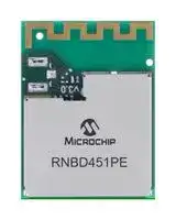


RNBD451PE-I100
Bluetooth Module, BLE 5.2, 2Mbps, PCB Antenna, 1.9 to 3.6V, -102dBm, -40 to 85 °C, RNBD451 Series
- Manufacturer: MICROCHIP
- Product type: Bluetooth Modules & Adaptors
- SVHC: No SVHC (04-Feb-2026)
- Interfaces: UART
- Product Range: RNBD451 Series
- Certifications: CE, FCC, ISED, KC, MIC, NCC, SRRC, UKCA
- Bluetooth Class: -
- Bluetooth Version: Bluetooth LE 5.2
- Supply Voltage Range: 1.9 V to 3.6 V
- Receiver Sensitivity Rx: -102 dBm
- Operating Temperature Range: -40 °C to 85 °C
| Delivery and price | |
|---|---|
| Units per pack | 490 |
| Price | 2.96 € |
| Current stock | 10+ |
| Lead time | 30 days |
## **RNBD451 Bluetooth[®] Low Energy Module Data Sheet RNBD451**

## **Introduction**

The RNBD451 module is based on Microchip’s PIC32CX-BZ2 Bluetooth® Low Energy System-on-Chip (SoC) that provides a complete solution to implement Bluetooth 5.2 Low Energy connectivity. These modules are interfaced via a Two-Wire or Four-Wire (Flow Control) UART interface with Microchip’s simple ASCII command set for easy integration into most of the applications. The host microcontroller can dynamically configure the RNBD451 module with a few simple ASCII commands. The RNBD451 module, combined with Microchip’s Bluetooth Low Energy silicon with necessary GPIO and an on-board PCB antenna, creates an easy-to-use drop-in solution.

## **Features**

- Fully RF-Certified Bluetooth Low Energy Module

- Compact Form Factor

- On-Board Bluetooth 5.2 Low Energy Stack

- ASCII Command Interface Over UART

- Host Controller Interface (HCI) Mode

- ASCII Commands are Backward Compatible with RN487x Family of Modules

- Beacon Support

- Built-in Microchip Transparent Profile for UART Data Streaming

- Over-the-Air (OTA) Remote Configuration

- Embedded Enhanced Security

- 2M Uncoded PHY and Long Range (Coded PHY)

- Extended Advertising

- Data Length Extensions and Secure Connections

- Bluetooth Low Energy Privacy 1.2 with Up to Eight Resolvable and Accept Lists

- UART-Based Device Firmware Update (DFU)

- Built-in Microchip OTA Profile with Client and Server Role for OTA DFU Execution

   - OTA device firmware update

   - OTAPC device firmware update on peer RNBD451 device

   - Host MCU OTA firmware update using RNBD451

- Integrated 16 MHz POSC

- Supports UART

- Eight GPIOs that Can Be Controlled By RN Command

- 12-Bit Analog-to-Digital Converters (ADC) Successive Approximation Register (SAR) Module for Analog-toDigital Conversion

- Add-On Up to Six 16-Bit UUID GATT Services (Public Service), Four 128-Bit UUID GATT Services (Private Service) and Each Service Includes Up to Eight Characteristic Attributes

Advance Information Data Sheet

DS70005514B - 1

© 2022-2023 Microchip Technology Inc. and its subsidiaries

**RNBD451**

- Supports Bluetooth Low Energy Advertiser, Observer, Central and Peripheral Roles

- Supports Bluetooth Low Energy GATT Client and Server Roles

- Supports Up to Six Concurrent Bluetooth Low Energy Connections

- Multi-Link and Multi-Role

- Remote Command Mode in Multi-Link Connection

- Secured Connection

- DTM Test Mode

- Supports PTA Control

Advance Information Data Sheet

DS70005514B - 2

© 2022-2023 Microchip Technology Inc. and its subsidiaries

**RNBD451**

## **Operational Conditions**

- Operating Voltage:

   - 3.3V typical

   - MLDO mode (Linear Regulator): 1.9V - 3.6V

   - DC-DC mode (Buck Regulator): 2.4V - 3.6V

- Temperature Range: -40°C to +85°C

- 39-pin SMD Package with Shield CAN

   - Size: 15.5 mm x 20.7 mm x 2.8 mm

## **RF/Analog Features**

- Industrial, Scientific and Medical (ISM) Band: 2.402-2.480 GHz Operation

- Channels: 0-39

- Up to +15 dBm E.I.R.P Programmable Transmit Output Power

- Typical Receiver Power Sensitivity:

   - -95 dBm for Bluetooth Low Energy 1 Mbps

   - -92 dBm for Bluetooth Low Energy 2 Mbps

   - -102 dBm for Bluetooth Low Energy 125 Kbps

   - -99 dBm for Bluetooth Low Energy 500 Kbps

- Digital Received Signal Strength Indicator (RSSI)

## **Applications**

- Health/Medical Devices

- Sports Activity/Fitness Meters

- Beacon Applications

- Internet of Things (IoT) Sensor Tag

- Remote Control

- Wearable Smart Devices and Accessories

- Smart Energy/Smart Home

- Industrial Control

Advance Information Data Sheet

DS70005514B - 3

© 2022-2023 Microchip Technology Inc. and its subsidiaries

**RNBD451**

## **Table of Contents**

|**Table of Contents**|**Table of Contents**|**Table of Contents**|
|---|---|---|
|Introduction...........................................................................................................................................................................1|||
|Features................................................................................................................................................................................. 1|||
||Operational Conditions................................................................................................................................................ 3||
||RF/Analog Features ...................................................................................................................................................... 3||
||Applications ...................................................................................................................................................................3||
|1.|Quick References...........................................................................................................................................................6||
||1.1.|Reference Documentation................................................................................................................................6|
||1.2.|Acronyms and Abbreviations............................................................................................................................6|
|2.|Ordering Information....................................................................................................................................................7||
||2.1.|RNBD451 Module Ordering Information........................................................................................................ 7|
|3.|Device Overview............................................................................................................................................................ 8||
||3.1.|Module Overview............................................................................................................................................... 8|
||3.2.|Module Confguration .................................................................................................................................... 10|
||3.3.|Device Power Modes....................................................................................................................................... 12|
||3.4.|Device Programming....................................................................................................................................... 13|
|4.|Electrical Characteristics.............................................................................................................................................14||
||4.1.|Absolute Maximum Electrical Characteristics.............................................................................................. 14|
||4.2.|DC Electrical Characteristics........................................................................................................................... 14|
||4.3.|Active Current Consumption DC Electrical Specifcations.......................................................................... 15|
||4.4.|Sleep Current Consumption DC Electrical Specifcations........................................................................... 16|
||4.5.|Deep Sleep Current Consumption DC Electrical Specifcations................................................................. 18|
||4.6.|XDS (Extreme Deep Sleep) Current Consumption DC Electrical Specifcations....................................... 18|
||4.7.|Power Supply DC Module Electrical Specifcations......................................................................................19|
||4.8.|I/O PIN AC/DC Electrical Specifcations......................................................................................................... 20|
||4.9.|ADC Electrical Specifcations...........................................................................................................................22|
||4.10.|Bluetooth Low Energy RF Characteristics..................................................................................................... 23|
|5.|Basic|Connection Requirement................................................................................................................................. 35|
||5.1.|Power Pins........................................................................................................................................................ 35|
||5.2.|Master Clear (NMCLR) Pin...............................................................................................................................35|
||5.3.|Unused I/O Pins............................................................................................................................................... 36|
||5.4.|Interface Pins....................................................................................................................................................36|
|6.|Physical Dimensions and Attributes......................................................................................................................... 37||
||6.1.|RNBD451 Module Placement Guidelines......................................................................................................37|
||6.2.|RNBD451 Module Routing Guidelines.......................................................................................................... 38|
||6.3.|RNBD451 Module Packaging Information ................................................................................................... 39|
||6.4.|RNBD451 Module RF Considerations............................................................................................................42|
||6.5.|RNBD451 Module Antenna Considerations................................................................................................. 43|
||6.6.|RNBD451 Module Refow Profle Information..............................................................................................43|
||6.7.|RNBD451 Module Assembly Considerations................................................................................................43|
|7.|ASCII|Command API.................................................................................................................................................... 45|


Advance Information Data Sheet © 2022-2023 Microchip Technology Inc. and its subsidiaries

DS70005514B - 4

**RNBD451**

|8.|Application Reference Schematics............................................................................................................................ 46|
|---|---|
|9.|Supported Bluetooth Low Energy Profle and Services ......................................................................................... 47|
|10.|Appendix A: Regulatory Approval..............................................................................................................................48|
||10.1. United States.................................................................................................................................................... 48|
||10.2. Canada.............................................................................................................................................................. 49|
||10.3. Europe............................................................................................................................................................... 50|
||10.4. Japan..................................................................................................................................................................51|
||10.5. Korea................................................................................................................................................................. 52|
||10.6. Taiwan............................................................................................................................................................... 52|
||10.7. China..................................................................................................................................................................53|
||10.8. UKCA (UK Conformity Assessed)....................................................................................................................53|
||10.9. Other Regulatory Information........................................................................................................................54|
|11.|Document Revision History........................................................................................................................................55|
|Microchip Information....................................................................................................................................................... 57||
||The Microchip Website............................................................................................................................................... 57|
||Product Change Notifcation Service........................................................................................................................ 57|
||Customer Support.......................................................................................................................................................57|
||Microchip Devices Code Protection Feature............................................................................................................ 57|
||Legal Notice..................................................................................................................................................................57|
||Trademarks.................................................................................................................................................................. 58|
||Quality Management System.....................................................................................................................................59|
||Worldwide Sales and Service..................................................................................................................................... 60|


Advance Information Data Sheet

DS70005514B - 5

© 2022-2023 Microchip Technology Inc. and its subsidiaries

**RNBD451 Quick References**

## **1. Quick References**

## **1.1 Reference Documentation**

For more details, refer to the following documents:

- _AN233 Solder Reflow Recommendation Application Note_ (DS00233)

- _RNBD451 Bluetooth[®] Low Energy Module User’s Guide_ (DS50003467)

## **1.2 Acronyms and Abbreviations**

**Table 1-1.** Acronyms and Abbreviations

|**Acronyms and Abbreviations**|**Description**|
|---|---|
|ADC|Analog-to-Digital Converters|
|API|Application Programming Interface|
|CDM|Charged Device Model|
|CTS|Clear to Send|
|DIS|Device Information Service|
|DFU|Device Firmware Update|
|HBM|Human Body Model|
|IoT|Internet of Things|
|ISM|Industrial, Scientifc and Medical|
|MBD|Microchip Bluetooth Data|
|NVM|Nonvolatile Memory|
|OTA|Over-the-air|
|OTAPC|Over-the-air Profle Client|
|PDS|Persistent Data Storage|
|PMU|Power Management Unit|
|POR|Power-on Reset|
|RSSI|Received Signal Strength Indicator|
|RTS|Request to Send|
|SAR|Successive Approximation Register|
|SoC|System-on-Chip|


Advance Information Data Sheet

DS70005514B - 6

© 2022-2023 Microchip Technology Inc. and its subsidiaries

**RNBD451 Ordering Information**

## **2. Ordering Information**

This chapter provides the ordering information of the RNBD451 module.

## **2.1 RNBD451 Module Ordering Information**

The following table describes the ordering information of the RNBD451 module.

**Table 2-1.** RNBD451 Module Ordering Details

|**Model No.**|**Module SoC**|**Description**|**Regulatory**<br>**Certifcation**|**Ordering Code**|
|---|---|---|---|---|
|RNBD451PE|PIC32CX1012BZ25048-<br>I/MYX|RNBD451 module with<br>PCB antenna|FCC, ISED, CE, UKCA,<br>SRRC, KCC, MIC, NCC|RNBD451PE-IXXX|


The following figure illustrates the details of the RNBD451 module ordering information.

**Figure 2-1.** RNBD451 Module Ordering Information

**==> picture [415 x 250] intentionally omitted <==**

**----- Start of picture text -----**<br>
-<br>RN BD 45 1 P E I XXX<br>Microchip Brand<br>Technology<br>Bluetooth Data<br>Family<br>Pin Count<br>1 = High<br>Antenna<br>P = PCB Antenna<br>Encryption<br>E = Encryption<br>Temperature Range<br>I = Industrial (-40 to +85°C)<br>Firmware Version/<br>Custom Designation<br>**----- End of picture text -----**<br>


Advance Information Data Sheet

DS70005514B - 7

© 2022-2023 Microchip Technology Inc. and its subsidiaries

**RNBD451 Device Overview**

## **3. Device Overview**

## **3.1 Module Overview**

The RNBD451 Bluetooth Low Energy module integrates the Bluetooth 5.2 baseband controller, Bluetooth stack, digital and analog I/O and RF power amplifier into one solution.

## **Figure 3-1.** RNBD451 Module Block Diagram

**==> picture [456 x 232] intentionally omitted <==**

**----- Start of picture text -----**<br>
Printed<br>Antenna<br>Power Encryption Subsystem Wireless Subsystem<br>Power Supply DC-DC/MLDO Integrity Check Monitor<br>Radio Transceiver RF Matching<br>Storage and<br>CLDO AES Circuit<br>Filtering<br>Bandgap Public Key Crypto<br>Bluetooth<br>TRNG<br>16 MHz Cryst al  SERCOM USART<br>Oscillators Cortex [®]  M4 CPU<br>WDSP 64 MHz<br>GPIO/EIC GPIO<br>System Timer 1 MB Flash<br>Panel, 32 kB<br> NVR ADC Analog Pin<br>128 KB SRAM<br>**----- End of picture text -----**<br>


Advance Information Data Sheet

DS70005514B - 8

© 2022-2023 Microchip Technology Inc. and its subsidiaries

**RNBD451 Device Overview**

## **Figure 3-2.** Pin Diagram – RNBD451

**==> picture [261 x 330] intentionally omitted <==**

**----- Start of picture text -----**<br>
U1<br>RNBD451<br>1 GND PB4 39<br>2 GND PB1 38<br>3 NMCLR PB2 37<br>4 PB0 PA3 36<br>5 PB3 PA2 35<br>TPAD_GND<br>6 PB5 PA14 34<br>7 VDD_A PA13 33<br>8 GND PA10 32<br>9 PA11 PA7 31<br>10 PA12 PA9 30<br>11 GND PA8 29<br>12 PB6 VDD 28<br>13 PB7 VDD 27<br>PB8 PB9 PA4 PB10 PB11 GND PA0 PA1 PB12 PB13 PA5 PA6 GND<br>14 15 16 17 18 19 20 21 22 23 24 25 26<br>**----- End of picture text -----**<br>


**Note:** Ensure the exposed thermal pad (TPAD_GND) on the bottom of the module is connected to ground in the PCB.

**Table 3-1.** Pin Description

|**Pin Number**|**Name**|**RNBD451 Defnition**|**Type**|
|---|---|---|---|
|1|GND|Ground|—|
|2|GND|Ground|—|
|3|NMCLR|Reset|I|
|4|PB0|PTA control (WLAN ACTIVE)|I|
|5|PB3|Bluetooth®Low Energy status indication pin 1/2|O|
|6|PB5|Bluetooth status LED|O|
|7|VDD_A|VDDANA power supply|—|
|8|GND|Ground|—|
|9|PA11|Reserved. No Connect|—|
|10|PA12|Reserved. No Connect|—|
|11|GND|Ground|—|
|12|PB6|UART receive data|I|
|13|PB7|Bluetooth Low Energy status indication pin 2/2|O|
|14|PB8|I/O level control by RN command|I/O|
|15|PB9|Reserved. No Connect|—|
|16|PA4|UART Request to Send (RTS)|O|
|17|PB10|I/O level control by RN command|I/O|


Advance Information Data Sheet

DS70005514B - 9

© 2022-2023 Microchip Technology Inc. and its subsidiaries

**RNBD451 Device Overview**

|**...........continued**|**...........continued**|**...........continued**|**...........continued**|
|---|---|---|---|
|**Pin Number**|**Name**|**RNBD451 Defnition**|**Type**|
|18|PB11|I/O level control by RN command|I/O|
|19|GND|Ground|—|
|20|PA0|I/O level control by RN command|I/O|
|21|PA1|I/O level control by RN command|I/O|
|22|PB12|I/O level control by RN command|I/O|
|23|PB13|I/O level control by RN command|I/O|
|24|PA5|UART transmit data|O|
|25|PA6|UART Clear to Send (CTS)|I|
|26|GND|Ground|—|
|27|VDD|VDD and VDDIO power supply|—|
|28|VDD|VDD and VDDIO power supply|—|
|29|PA8|Debug UART receive data. Recommend to add<br>a test point on this pin.|I|
|30|PA9|Reserved|—|
|31|PA7|Debug UART transmit data. Recommend to<br>add a test point on this pin.|O|
|32|PA10|I/O level control by RN command|I/O|
|33|PA13|PTA control (BT_PRIORITY)|O|
|34|PA14|PTA control (BT_ACTIVE)|O|
|35|PA2|UART transmit indication pin|O|
|36|PA3|Event indication pin (RSSI indication pin)|O|
|37|PB2|UART mode switch|I|
|38|PB1|ADC|I|
|39|PB4|UART receive indication pin/RNBD451 wake-up<br>pin Low-power mode|I|
|**Notes:**<br>•<br>Upon reset, if the PB5 pin is held low, the RNBD451 module sends out REBOOT, MAC ID and frmware version. Upon the<br>RNBD451 module reset, the PB5 pin acts as the input for approximately 300 ms. Post this time, the PB5 pin changes to<br>output and resumes normal functionality, which is Bluetooth status LED.<br>•<br>It is recommend to have a 10K pull-up resistor on the UART TXD pin (PA5). For reference, see8.  Application Reference<br>Schematics.<br>•<br>For the serial DFU update, the UART pins PB6 (UART receive data) and PA5 (UART transmit data) is used.||||


## **3.2 Module Configuration**

Use the ASCII command interface for configuring the GPIO pins of the RNBD451 module to different functions. The following table provides the details about the various pins and functions in the RNBD451 module that are available for configuration and their default configuration settings. **Note:** This configuration is not applicable in HCI mode.

Advance Information Data Sheet

DS70005514B - 10

© 2022-2023 Microchip Technology Inc. and its subsidiaries

**RNBD451 Device Overview**

**Table 3-2.** Configurable Functions and Descriptions

|**Pin**|**Function**<br>**Name**|**Description**|
|---|---|---|
|PB5|Bluetooth®<br>status LED|To indicate the Bluetooth Low Energy connection status by a specifc LED fash pattern, see the<br>following pattern description:<br>•<br>Standby mode – No Bluetooth Low Energy connection. The RNBD451 module is in<br>Advertisement or Scan state. Flash one time for every three seconds.<br>–<br>ON – 50 ms<br>–<br>OFF – 2950 ms<br>•<br>Linked mode – Bluetooth Low Energy ACL link is connected, regardless of whether it is in the<br>Central or Peripheral role. Flash two times for every 1.5 seconds.<br>–<br>ON – 50 ms<br>–<br>OFF – 150 ms<br>–<br>ON – 50 ms<br>–<br>OFF – 1050 ms<br>•<br>DFU mode – The RNBD451 module is in MCU DFU procedure. Flash 4 times for every two<br>seconds.<br>–<br>ON – 100 ms<br>–<br>OFF – 100 ms<br>**Note:**By default, the Bluetooth status LED is turned OFF. The user can enable this feature by<br>using the`SR,<hex16>`command. For example`SR,0001`. For more details, refer to the_RNBD451_<br>_Bluetooth Low Energy Module User’s Guide_(DS50003467).|
|PB1|ADC|A dedicated ADC input pin where an analog signal can be the input to the RNBD451 module. The<br>RNBD451 module performs the ADC conversion using a fxed reference and provides the digital<br>value that can be read using a command. For more details, refer to the_RNBD451 Bluetooth Low_<br>_Energy Module User’s Guide_(DS50003467).|
|PB8,<br>PB10,<br>PB11,<br>PA0,<br>PA1,<br>PB12,<br>PB13<br>and<br>PA10|I/O level<br>control|Host MCU can assert the RN command to set some GPIO pins as output pins to set their level or<br>input pins to read their level.|
|PB2|UART mode<br>switch|•<br>When the host MCU pulls the UART mode switch pin from low to high (rising edge), the<br>RNBD451 module switches to the Data mode.<br>•<br>When the host MCU pulls the UART mode switch pin from high to low (falling edge), the<br>RNBD451 module switches to the Command mode.<br>•<br>When the host MCU uses the RN command to switch the mode, the host MCU keeps the UART<br>mode switch pin to the original setting.<br>**Note:**By default, the UART mode switch functionality is not assigned on to the PB2 pin. The<br>user can enable this feature using the`SR,<hex16>`command, for example,`SR,0002`. For<br>more details, refer to the_RNBD451 Bluetooth Low Energy Module User’s Guide_(DS50003467).|
|PB4|UART RX<br>indication|•<br>If the RNBD451 module’s low power is enabled, the host MCU must wake up the RNBD451<br>module before sending the UART data out.<br>•<br>Pull the UART RX indication pin low to wake up the system).|
|PA3|RSSI indication|•<br>Use this indication pin to indicate the quality of the link based on the RSSI level.<br>•<br>If the RSSI level is lower than the specifed threshold value, the RSSI indication pin goes low.|
|PA2|UART TX<br>indication|•<br>UART TX indication is an output pin. Provides indication if the RNBD451 module is transmitting<br>to host MCU over UART.<br>•<br>Pulled low before UART TX begins and pulled high after UART TX is over.|


Advance Information Data Sheet

DS70005514B - 11

© 2022-2023 Microchip Technology Inc. and its subsidiaries

**RNBD451 Device Overview**

**Table 3-3.** Status Indication Pins

|**BT_Status_Ind1 (PB3)**|**BT_Status_Ind2 (PB7)**|**RNBD451 Status**|
|---|---|---|
|Low|Low|Bluetooth®Low Energy is disconnected|
|||Data transmission channel is closed|
|High|Low|Bluetooth Low Energy is connected|
|||Data transmission channel is closed|
|High|High|Bluetooth Low Energy is connected|
|||Data transmission channel is opened|
|Low|High|DFU mode (local or Over-the-air Profle Client<br>(OTAPC))|
|**Note:**By default the Bluetooth status indication feature is disabled in the frmware. The user can enable this feature via<br>`SR,<hex16>`command, for example,`SR,1000`. For more details, refer to the_RNBD451 Bluetooth Low Energy Module User’s_<br>_Guide_(DS50003467).|||


## **3.3 Device Power Modes**

The RNBD451 module incorporates a Power Management Unit (PMU) that provides both DC-DC (Buck) and MLDO power conversion. On power-up, the RNBD451 module operates in MLDO mode. The RNBD451 module command set provides the option to set the PMU mode as MLDO mode or BUCK PWM mode via `Set PMU Mode` command. For example, `SPMU,<0,1>` .

The RNBD451 module supports the following device power modes:

- Run mode – In the Run mode, the CPU is actively executing code. Run mode provides normal operation of the processor. All the features and configurations are available to be controlled.

- Sleep/Standby mode – In this mode, the RNBD451 module operates with minimum power consumption. Upon entering this mode, the RNBD451 module enters into minimal power consumption state in between the advertisement interval. After establishing the connection, then in between the connection interval, the RNBD451 module enters into minimal power consumption state and only consumes less power. Every connection/advertising interval, the RNBD451 module wakes up from Sleep/Standby Sleep mode, performs the Bluetooth low energy activity and goes back to sleep. In this mode, the overall average power consumption of the system is always less in comparison to the module in Run mode. Use the `Low Power Control` command to configure the RNBD451 module into Sleep mode or Low-power Control mode. For example, `SO,<0,1>` .

Pull the UART_RX_IND (PB4) pin to low from Host MCU to enable the UART before the Host MCU transmits data to the RNBD451 module. The UART_RX_IND must be active prior to UART data more than two ms to make the RNBD451 module ready to receive data.

- Deep Sleep mode – In this mode, configure the RNBD451 module to operate with less power consumption compared to Sleep/Standby mode. The Deep Sleep mode feature is incorporated only for advertisement. After every advertising interval, the RNBD451 module wakes up from Deep Sleep mode, performs the advertisement and goes back to Deep Sleep mode. The RNBD451 module continues this pattern of advertisement until a connection is established. Enable the deep sleep advertisement in the RNBD451 module using `Set Deep Sleep Advertising` command. For example, `SDO,<0,1>,<hex16>` .

   - Pull the UART_RX_IND (PB4) pin to low from host MCU to enable the UART before Host MCU transmits data to the RNBD451 module. The UART_RX_IND must be active prior to UART data more than 25 ms to make the RNBD451 module ready to receive data.

- Extreme Deep Sleep mode – In this mode, configure the module to operate in Shutdown state. In this state, the system stays in the Extreme Deep Sleep (XDS) mode and it consumes extreme low power. Hard reset or pull UART_RX_IND pin low can bring the system back to Run mode. For more details on the commands for different Low-power mode configurations, refer to the _RNBD451 Bluetooth Low Energy Module User’s Guide_ (DS50003467).

Advance Information Data Sheet © 2022-2023 Microchip Technology Inc. and its subsidiaries

DS70005514B - 12

**RNBD451 Device Overview**

## **3.4 Device Programming**

The RNBD451 device is available for purchase with a pre-programmed firmware. Microchip periodically releases the firmware for fixing previously reported issues or to implement latest feature support. There are two ways to perform regular firmware update:

1. Serial DFU command based update over UART

2. Over-the-air (OTA) update of firmware using Microchip Bluetooth Data (MBD) mobile application or module to module OTA update (OTAPC mode commands)

3. Advanced programming

For advanced programming option (SWD), go to support.microchip.com.

**Note:** For the serial DFU and OTA programming guidance, refer to the _RNBD451 Bluetooth Low Energy Module User’s Guide_ (DS50003467).

Advance Information Data Sheet

DS70005514B - 13

© 2022-2023 Microchip Technology Inc. and its subsidiaries

**RNBD451 Electrical Characteristics**

## **4. Electrical Characteristics**

## **4.1 Absolute Maximum Electrical Characteristics**

Exposure to these maximum rating conditions for extended periods may affect device reliability. Functional operation of the device at these or any other conditions above the parameters indicated in the operation listings of this specification is not implied.

**Table 4-1.** Absolute Maximum Ratings

|**Parameter**|**Value**|
|---|---|
|Ambient temperature under bias|-40°C to +85°C|
|Storage temperature|-65°C to +150°C|
|Voltage on VDD/ VDDIOwith respect to GND|-0.3V to +4.0V|
|Voltage on pins, with respect to GND|-0.3V to (VDD+ 0.3V)|
|Maximum current out of GND pins|300 mA|
|Maximum current into VDDpins(2)|300 mA|
|Maximum output current sourced/sunk by any Low Current Mode I/O pin (4x drive<br>strength)|10 mA|
|Maximum output current sourced/sunk by any High Current Mode I/O pin (8x drive<br>strength)|15 mA|
|Maximum current sink by all ports|120 mA|
|Maximum current sourced by all ports(2)|120 mA|
|**ESD Qualifcation**||
|Human Body Model (HBM) per JESD22-A114|2000V|
|Charged Device Model (CDM) (ANSI/ESD STM 5.3.1)…(All pins/Corner pins)|+500V/-500V|
|**Notes:**<br>1.<br>Stresses above those listed under “Absolute Maximum Ratings” can cause permanent damage to the device. This is a<br>stress rating only and functional operation of the device at those or any other conditions above those indicated in the<br>operation listings of this specifcation is not implied. Exposure to the maximum rating conditions for extended periods<br>may afect device reliability.<br>2.<br>Maximum allowable current is a function of device maximum power dissipation (See the_Thermal Operating Conditions_<br>table in the_Thermal Specifcations_from Related Links).||


## **4.2 DC Electrical Characteristics**

**Table 4-2.** Operating Frequency VS. Voltage

|**Param. No.**|**VDDIO, VDDANA Range**|**Temp. Range (in °C)**|**Max. MCU Frequency**|**Comments**|
|---|---|---|---|---|
|DC_5|1.9V to 3.6V|-40°C to +85°C|64 MHz|Industrial|
|**Notes:**<br>1.<br>The same voltage must be applied to VDDINand VDDANA.<br>2.<br>MLDO mode (Linear regulator): 1.9V - 3.6V<br>DC-DC mode (Buck regulator): 2.4V - 3.6V|||||


Advance Information Data Sheet

DS70005514B - 14

© 2022-2023 Microchip Technology Inc. and its subsidiaries

**RNBD451 Electrical Characteristics**

## **4.3 Active Current Consumption DC Electrical Specifications**

**Table 4-3.** Active Current Consumption DC Electrical Specifications

|**DC Characteristics**|**DC Characteristics**|||**Standard Operating Conditions: VDDIO = VDDANA**<br>**1.9V to 3.6V (unless otherwise stated) Operating**<br>**Temperature: -40°C ≤ TA ≤ +85°C for Industrial Temp**|**Standard Operating Conditions: VDDIO = VDDANA**<br>**1.9V to 3.6V (unless otherwise stated) Operating**<br>**Temperature: -40°C ≤ TA ≤ +85°C for Industrial Temp**|**Standard Operating Conditions: VDDIO = VDDANA**<br>**1.9V to 3.6V (unless otherwise stated) Operating**<br>**Temperature: -40°C ≤ TA ≤ +85°C for Industrial Temp**|**Standard Operating Conditions: VDDIO = VDDANA**<br>**1.9V to 3.6V (unless otherwise stated) Operating**<br>**Temperature: -40°C ≤ TA ≤ +85°C for Industrial Temp**|
|---|---|---|---|---|---|---|---|
|**Param. No.**|**Symbol**|**Characteristics**|**Clock/Freq**|**Typ(1)**|**Max.**|**Units**|**Conditions**|
|APWR_1|IDD_ACTIVE|MCU IDDin Active<br>|PLL 64 MHz|131|—|μA/MHz|VDD= VDDANA|
|APWR_2||mode w/LDO<br>mode selected|FRC 8 MHz|443|||= 3.3V|
|APWR_3||MCU IDDin Active<br>mode w/BUCK<br>mode selected|PLL 64 MHz|76.8||||
|APWR_4|||FRC 8 MHz|300||||


**Figure 4-1.** Run Mode Current Consumption in Buck Mode at PLL 64 MHz

**==> picture [461 x 241] intentionally omitted <==**

**----- Start of picture text -----**<br>
7<br>6<br>5<br>2.4 - 64<br>2.7 - 64<br>4 3.3 - 64<br>3.6 - 64<br>3<br>2<br>1<br>0<br>-40 0 25 60 85<br>Temperature (in degree Celcius)<br>Current Consumption (mA)<br>**----- End of picture text -----**<br>


Advance Information Data Sheet

DS70005514B - 15

© 2022-2023 Microchip Technology Inc. and its subsidiaries

**RNBD451 Electrical Characteristics**

**Figure 4-2.** Run Mode Current Consumption in MLDO Mode at PLL 64 MHz

**==> picture [459 x 225] intentionally omitted <==**

**----- Start of picture text -----**<br>
9.2<br>9<br>8.8<br>8.6<br>1.9 - 64<br>8.4 2.4 - 64<br>2.7 - 64<br>3.3 - 64<br>8.2<br>3.6 - 64<br>8<br>7.8<br>7.6<br>7.4<br>7.2<br>7<br>-40 0 25 60 85<br>Temperature (in degree Celcius)<br>Current Consumption (mA)<br>**----- End of picture text -----**<br>


## **Note:**

1. Typical value measured at 3.3V and 25 ℃

## **4.4 Sleep Current Consumption DC Electrical Specifications**

**Table 4-4.** Sleep Current Consumption DC Electrical Specifications

|**DC Characteristics**|**DC Characteristics**||**Standard Operating Conditions: VDDIO = VDDANA 1.9V to 3.6V (unless**<br>**otherwise stated) Operating Temperature: -40°C ≤ TA ≤ +85°C for**<br>**Industrial Temp**|**Standard Operating Conditions: VDDIO = VDDANA 1.9V to 3.6V (unless**<br>**otherwise stated) Operating Temperature: -40°C ≤ TA ≤ +85°C for**<br>**Industrial Temp**|**Standard Operating Conditions: VDDIO = VDDANA 1.9V to 3.6V (unless**<br>**otherwise stated) Operating Temperature: -40°C ≤ TA ≤ +85°C for**<br>**Industrial Temp**|**Standard Operating Conditions: VDDIO = VDDANA 1.9V to 3.6V (unless**<br>**otherwise stated) Operating Temperature: -40°C ≤ TA ≤ +85°C for**<br>**Industrial Temp**|**Standard Operating Conditions: VDDIO = VDDANA 1.9V to 3.6V (unless**<br>**otherwise stated) Operating Temperature: -40°C ≤ TA ≤ +85°C for**<br>**Industrial Temp**|
|---|---|---|---|---|---|---|---|
|**Param. No.**|**Symbol**|**Characteristics**|**VDDIO**|**Typ(1)**|**Max.**|**Units**|**Conditions**|
|SPWR_1|IDD_SLEEP|MCU IDDin Sleep<br>mode w/LDO<br>mode selected|3.3V|950|—|µA|XTAL ON|
|SPWR_29||MCU IDDin Sleep<br>mode w/BUCK<br>mode selected|3.3V|470|—|µA|XTAL ON|


Advance Information Data Sheet

DS70005514B - 16

© 2022-2023 Microchip Technology Inc. and its subsidiaries

**RNBD451 Electrical Characteristics**

## **Figure 4-3.** Sleep Current with XTAL_ON_MLDO

**==> picture [459 x 300] intentionally omitted <==**

**----- Start of picture text -----**<br>
5<br>4.5<br>4<br>3.5<br>3 1.9<br>2.4<br>2.5<br>2.7<br>2<br>3.3<br>1.5 3.6<br>1<br>0.5<br>0<br>-40 0 25 60 85<br>Temperature (DegreeC)<br>IDD_Total_Current (mA)<br>**----- End of picture text -----**<br>


**Figure 4-4.** Sleep Current with XTAL_ON_DC_DC

**==> picture [458 x 154] intentionally omitted <==**

**----- Start of picture text -----**<br>
5<br>2.4<br>4.5<br>2.7<br>4<br>3.5 3.3<br>3 3.6<br>2.5<br>2<br>1.5<br>1<br>0.5<br>0<br>-40 0 25 60 85<br>Temperature (DegreeC)<br>IDD_Total_Current (mA)<br>**----- End of picture text -----**<br>


## **Note:**

1. Typical value measured during characterization at 3.3V and 25 ℃

Advance Information Data Sheet

DS70005514B - 17

© 2022-2023 Microchip Technology Inc. and its subsidiaries

**RNBD451 Electrical Characteristics**

## **4.5 Deep Sleep Current Consumption DC Electrical Specifications**

**Table 4-5.** Deep Sleep Current Consumption DC Electrical Specifications

|**DC Characteristics**|**DC Characteristics**|**DC Characteristics**|**Standard Operating Conditions: VDDIO = VDDANA 1.9V to 3.6V (unless**<br>**otherwise stated) Operating Temperature: -40°C ≤ TA ≤ +85°C for Industrial**<br>**Temp**|**Standard Operating Conditions: VDDIO = VDDANA 1.9V to 3.6V (unless**<br>**otherwise stated) Operating Temperature: -40°C ≤ TA ≤ +85°C for Industrial**<br>**Temp**|**Standard Operating Conditions: VDDIO = VDDANA 1.9V to 3.6V (unless**<br>**otherwise stated) Operating Temperature: -40°C ≤ TA ≤ +85°C for Industrial**<br>**Temp**|**Standard Operating Conditions: VDDIO = VDDANA 1.9V to 3.6V (unless**<br>**otherwise stated) Operating Temperature: -40°C ≤ TA ≤ +85°C for Industrial**<br>**Temp**|**Standard Operating Conditions: VDDIO = VDDANA 1.9V to 3.6V (unless**<br>**otherwise stated) Operating Temperature: -40°C ≤ TA ≤ +85°C for Industrial**<br>**Temp**|
|---|---|---|---|---|---|---|---|
|**Param.**<br>**No.**|**Symbol**|**Characteristics**|**VDDIO**|**Typ(1)**|**Max.**|**Units**|**Conditions**|
|BPWR_1|IDD_BACKUP|MCU IDDin Deep<br>Sleep mode powered<br>|3.3V|1.2|—|µA|No backup RAM<br>retained|
|BPWR_2||from VDDIO|3.3V|1.5|—|µA|8 KB backup RAM<br>retained|
|**Figure 4-5.**Deep Sleep Current RAM ON<br>**Current in μA**<br>**Temperature (°C)**<br>0<br>0.5<br>1<br>1.5<br>2<br>2.5<br>3<br>3.5<br>-40<br>0<br>25<br>60<br>85<br>1.9<br>2.4<br>2.7<br>3.3<br>3.6||||||||


## **Note:**

1. Typical value measured during characterization at 3.3V and 25 ℃

## **4.6 XDS (Extreme Deep Sleep) Current Consumption DC Electrical Specifications**

**Table 4-6.** XDS (Extreme Deep Sleep) Current Consumption DC Electrical Specifications

|**DC Characteristics**|**DC Characteristics**|**DC Characteristics**|**Standard Operating Conditions: VDDIO = VDDANA 1.9V to 3.6V (unless otherwise**<br>**stated) Operating Temperature: -40°C ≤ TA ≤ +85°C for Industrial Temp**|**Standard Operating Conditions: VDDIO = VDDANA 1.9V to 3.6V (unless otherwise**<br>**stated) Operating Temperature: -40°C ≤ TA ≤ +85°C for Industrial Temp**|**Standard Operating Conditions: VDDIO = VDDANA 1.9V to 3.6V (unless otherwise**<br>**stated) Operating Temperature: -40°C ≤ TA ≤ +85°C for Industrial Temp**|**Standard Operating Conditions: VDDIO = VDDANA 1.9V to 3.6V (unless otherwise**<br>**stated) Operating Temperature: -40°C ≤ TA ≤ +85°C for Industrial Temp**|**Standard Operating Conditions: VDDIO = VDDANA 1.9V to 3.6V (unless otherwise**<br>**stated) Operating Temperature: -40°C ≤ TA ≤ +85°C for Industrial Temp**|
|---|---|---|---|---|---|---|---|
|**Param.**<br>**No.**|**Symbol **|**Characteristics**|**VDDIO**|**Typ(1)**|**Max.**|**Units**|**Conditions**|
|OPWR_1|IDD_OFF|MCU IDDin OFF<br>mode powered<br>from VDDIOx|3.3V|0.12|—|µA|In OFF mode, the<br>device is entirely<br>powered-of.|


Advance Information Data Sheet

DS70005514B - 18

© 2022-2023 Microchip Technology Inc. and its subsidiaries

**RNBD451 Electrical Characteristics**

## **Figure 4-6.** Extreme Deep Sleep Current

**==> picture [457 x 214] intentionally omitted <==**

**----- Start of picture text -----**<br>
1.2<br>1<br>0.8<br>1.9<br>0.6 2.4<br>2.7<br>3.3<br>0.4 3.6<br>0.2<br>0<br>-40 0 25 60 85<br>Temperature (°C)<br>Current in μA<br>**----- End of picture text -----**<br>


## **Note:**

1. Typical value measured during characterization at 3.3V and 25 ℃

## **4.7 Power Supply DC Module Electrical Specifications**

**Table 4-7.** Power Supply DC Electrical Specifications

|**AC Characteristics**|**AC Characteristics**|**AC Characteristics**|**Standard Operating Conditions: VDDIO = VDDANA 1.9-3.6V (unless**<br>**otherwise stated)**<br>**Operating Temperature: -40°C ≤ TA ≤ +85°C for Industrial Temp**|**Standard Operating Conditions: VDDIO = VDDANA 1.9-3.6V (unless**<br>**otherwise stated)**<br>**Operating Temperature: -40°C ≤ TA ≤ +85°C for Industrial Temp**|**Standard Operating Conditions: VDDIO = VDDANA 1.9-3.6V (unless**<br>**otherwise stated)**<br>**Operating Temperature: -40°C ≤ TA ≤ +85°C for Industrial Temp**|**Standard Operating Conditions: VDDIO = VDDANA 1.9-3.6V (unless**<br>**otherwise stated)**<br>**Operating Temperature: -40°C ≤ TA ≤ +85°C for Industrial Temp**|**Standard Operating Conditions: VDDIO = VDDANA 1.9-3.6V (unless**<br>**otherwise stated)**<br>**Operating Temperature: -40°C ≤ TA ≤ +85°C for Industrial Temp**|
|---|---|---|---|---|---|---|---|
|**Param. No.**|**Symbol**|**Characteristics**|**Min.**|**Typ.**|**Max.**|**Units**|**Conditions**|
|REG_36|VDDCORE|VDDCORE voltage<br>range|—|1.2|—|V|—|
|REG_37|VDD(1)|VDD input voltage<br>range|1.9|3.3|3.6|V|—|
|REG_39|VDDANA(1)|VDDANA input<br>voltage range|1.9|3.3|3.6|V|—|
|REG_43|SVDDIO_R|VDDIO rise ramp<br>rate to ensure<br>internal Power-on<br>Reset signal|—|0.1|—|V/µs|Failure to meet this<br>specifcation may lead to<br>start-up or unexpected<br>behaviors|
|REG_44|SVDDIO_F|VDDIO falling ramp<br>rate to ensure<br>internal Power-on<br>Reset signal|—|—|—|V/µs|Failure to meet this<br>specifcation may cause the<br>device to not detect reset|
|REG_45|VP0R+|Power-on Reset|—|1.5|—|V|VDDIO power-up/down (See<br>Param REG43, VDDIO Ramp<br>Rate)|
|REG_45_A|VP0R-|Power-on Reset|—|1.5|—|V|VDDIO Power-up/down (See<br>Param REG43, VDDIO Ramp<br>Rate)|
|REG_47|VBOR33(1)|VDDIO BOR (All<br>modes)(1)|—|1.7|—|V|—|
|REG_48|VBOR12|BOR of the 1.2V<br>regulator|—|1.0|—|V|—|


Advance Information Data Sheet

DS70005514B - 19

© 2022-2023 Microchip Technology Inc. and its subsidiaries

**RNBD451 Electrical Characteristics**

|**...........continued**|**...........continued**|**...........continued**|**...........continued**|**...........continued**|**...........continued**|**...........continued**|**...........continued**|
|---|---|---|---|---|---|---|---|
|**AC Characteristics**|||**Standard Operating Conditions: VDDIO = VDDANA 1.9-3.6V (unless**<br>**otherwise stated)**<br>**Operating Temperature: -40°C ≤ TA ≤ +85°C for Industrial Temp**|||||
|**Param. No.**|**Symbol**|**Characteristics**|**Min.**|**Typ.**|**Max.**|**Units**|**Conditions**|
|REG_48A|VZBPOR33|Zero power BOR|—|1.8|—|V|—|
|REG_53|TRST(2)|External RESET valid<br>active pulse width|—|11|—|µs|Minimum Reset active time<br>to guarantee module Reset.<br>Reset flter circuit inside<br>Module|
|REG_58|BOR_DELAY|Width of the BOR<br>event|—|488|—|µs|—|
|**Notes:**<br>1.<br>VDD and VDDANA must be at the same voltage level.<br>2.<br>The RESET pulse width is the minimum pulse width required on the NMCLR pin after any fltering.||||||||


## **4.8 I/O PIN AC/DC Electrical Specifications**

**Table 4-8.** I/O PIN AC/DC Electrical Specifications

|**AC Characteristics**|**AC Characteristics**||**Standard Operating Conditions: VDDIO = VDDANA 1.9-3.6V (unless**<br>**otherwise stated)**<br>**Operating Temperature: -40°C ≤ TA ≤ +85°C for Industrial Temp**|**Standard Operating Conditions: VDDIO = VDDANA 1.9-3.6V (unless**<br>**otherwise stated)**<br>**Operating Temperature: -40°C ≤ TA ≤ +85°C for Industrial Temp**|**Standard Operating Conditions: VDDIO = VDDANA 1.9-3.6V (unless**<br>**otherwise stated)**<br>**Operating Temperature: -40°C ≤ TA ≤ +85°C for Industrial Temp**|**Standard Operating Conditions: VDDIO = VDDANA 1.9-3.6V (unless**<br>**otherwise stated)**<br>**Operating Temperature: -40°C ≤ TA ≤ +85°C for Industrial Temp**|**Standard Operating Conditions: VDDIO = VDDANA 1.9-3.6V (unless**<br>**otherwise stated)**<br>**Operating Temperature: -40°C ≤ TA ≤ +85°C for Industrial Temp**|
|---|---|---|---|---|---|---|---|
|**Param. No.**|**Symbol**|**Characteristics**|**Min.**|**Typ.(1)**|**Max.**|**Units**|**Conditions**|
|DI_1|VOL|Output voltage low<br>(Drive strength, 8x)|—|0.1|—|V|VDDIO = 3.3V at IOL = 10<br>mA|
|||Output voltage low<br>(Drive strength, 4x)||0.2|—||VDDIO = 3.3V at IOL = 10<br>mA|
|DI_2|VOL|Output voltage low<br>(Drive strength, 8x)|—|0.2|—|V|VDDIO = 3.3V at IOL = 13<br>mA|
|||Output voltage low<br>(Drive strength, 4x)||0.3|—||VDDIO = 3.3V at IOL = 13<br>mA|
|DI_3|VOL|Output voltage low<br>(Drive strength, 8x)|—|0.2|—|V|VDDIO = 3.3V at IOL = 15<br>mA|
|DI_4|VOH|Output voltage high<br>(Drive strength, 8x)|—|2.3|—|V|VDDIO = 3.3V at IOH = 5 mA|
|||Output voltage high<br>(Drive strength, 4x)|—|2.1|—||VDDIO = 3.3V at IOH = 5 mA|
|DI_5|VOH|Output voltage high<br>(Drive strength, 8x)|—|2.2|—|V|VDDIO = 3.3V at IOH = 7 mA|
|||Output voltage high<br>(Drive strength, 4x)|—|2.0|—||VDDIO = 3.3V at IOH = 7 mA|
|DI_6|VOH|Output voltage high<br>(Drive strength, 8x)|—|2.1|—|V|VDDIO = 3.3V at IOH = 10<br>mA|
|DI_7|VIL|Input voltage low<br>(Drive strength, 8x)|—|0.7|—|V|VDDIO = 3.3V|
|||Input voltage low<br>(Drive strength, 4x)|—|0.5|—||VDDIO = 3.3V|
|DI_8|VIH|Input voltage high<br>(Drive strength, 8x)|—|2.9|—|V|VDDIO = 3.3V|
|||Input voltage high<br>(Drive strength, 4x)|—|2.9|—||VDDIO = 3.3V|
|DI_13|IIL|Input pin leakage<br>current|—|71.8|—|nA|—|


Advance Information Data Sheet

DS70005514B - 20

© 2022-2023 Microchip Technology Inc. and its subsidiaries

**RNBD451 Electrical Characteristics**

|**...........continued**|**...........continued**|||||||
|---|---|---|---|---|---|---|---|
|**AC Characteristics**|||**Standard Operating Conditions: VDDIO = VDDANA 1.9-3.6V (unless**<br>**otherwise stated)**<br>**Operating Temperature: -40°C ≤ TA ≤ +85°C for Industrial Temp**|||||
|**Param. No.**|**Symbol**|**Characteristics**|**Min.**|**Typ.(1)**|**Max.**|**Units**|**Conditions**|
|DI_15(5)|RPDWN|Internal pull-down<br>(Drive strength, 8x)|—|21.4|—|kΩ|VDDIO = 3.3V|
|||Internal pull-down<br>(Drive strength, 4x)|—|3.9|—|kΩ||
|DI_17|RPUP|Internal pull-up<br>(Drive strength, 8x)|—|18.6|—|kΩ||
|||Internal pull-up<br>(Drive strength, 4x)|—|3.3|—|kΩ||
|DI_25|TRISE|I/O pin rise<br>time (High drive<br>strength, high load)|—|1.97|—|ns|VDDIO = 3.3V|
|||I/O pin rise time<br>(Low drive strength,<br>high load)|—|10.7|—|ns|—|
|||I/O pin rise<br>time (High drive<br>strength, standard<br>load)|—|2.0|—|ns|—|
|||I/O pin rise time<br>(Low drive strength,<br>standard load)|—|7.6|—|ns|—|
|DI_27|TFALL|I/O pin fall<br>time (High drive<br>strength, high load)|—|1.6|—|ns|—|
|||I/O pin fall time<br>(Low drive strength,<br>high load)|—|8.1|—|ns|—|
|||I/O pin fall<br>time (High drive<br>strength, standard<br>load)|—|1.6|—|ns|—|
|||I/O pin fall time<br>(Low drive strength,<br>standard load)|—|5.1|—|ns|—|


## **Notes:**

1. All measurements done at 3.3V at 25 ℃

2. VIL source < (GND – 0.3). Characterized but not tested.

3. Any number and/or combination of I/O pins not excluded under IICL or IICH conditions are permitted provided the absolute instantaneous sum of the input injection currents from all pins do not exceed the specified ∑IICT limit. To limit the injection current, the user must insert a resistor in series RSERIES (in other words, RS), between the input source voltage and device pin. The resistor value is calculated according to:

   - For negative Input voltages less than (GND – 0.3): RS ≥ absolute value of | ((VIL source – (GND – 0.3)) / IICL)

   - For positive input voltages greater than (VDDIO + 0.3): RS ≥ ((VIH source – (VDDIO +0.3))/ IICH)

   - For Vpin voltages greater than VDDIO + 0.3 and less than GND – 0.3: RS = the larger of the values calculated above

Advance Information Data Sheet

DS70005514B - 21

© 2022-2023 Microchip Technology Inc. and its subsidiaries

**RNBD451 Electrical Characteristics**

4. High load = 50 pF and Standard load = 30 pF

5. The drive strength of pads are as follows:

   - 8x pads - PA0, PA1, PA3, PA4, PA5, PA6, PA7, PA8, PA9, PA10, PA13, PA14, PB10, PB11, PB12, PB13

   - 4x pads - PA2, PB0, PB1, PB2, PB3, PB4, PB5, PB6, PB7, PB8, PB9

## **4.9 ADC Electrical Specifications**

**Table 4-9.** ADC AC Electrical Specifications

|**AC Characteristics**|**AC Characteristics**|**AC Characteristics**|**Standard Operating Conditions: VDDIO = VDDANA 1.9-3.6V (unless otherwise**<br>**stated)**<br>**Operating Temperature: -40°C ≤ TA ≤ +85°C for Industrial Temp**|**Standard Operating Conditions: VDDIO = VDDANA 1.9-3.6V (unless otherwise**<br>**stated)**<br>**Operating Temperature: -40°C ≤ TA ≤ +85°C for Industrial Temp**|**Standard Operating Conditions: VDDIO = VDDANA 1.9-3.6V (unless otherwise**<br>**stated)**<br>**Operating Temperature: -40°C ≤ TA ≤ +85°C for Industrial Temp**|**Standard Operating Conditions: VDDIO = VDDANA 1.9-3.6V (unless otherwise**<br>**stated)**<br>**Operating Temperature: -40°C ≤ TA ≤ +85°C for Industrial Temp**|**Standard Operating Conditions: VDDIO = VDDANA 1.9-3.6V (unless otherwise**<br>**stated)**<br>**Operating Temperature: -40°C ≤ TA ≤ +85°C for Industrial Temp**|
|---|---|---|---|---|---|---|---|
|**Param.**<br>**No.**|**Symbol **|**Characteristics**|**Min.**|**Typ.**|**Max.**|**Units**|**Conditions**|
|**Device Supply**||||||||
|ADC_1|VDDANA|ADC supply|VDDANA(min)|—|VDDANA(max)|V|VDDIO= VDDANA|
|**Reference Input**||||||||
|ADC_3|VREF(6)|ADC reference<br>voltage(4)|—|—|VDDANA|V|VREF= VDDANA|
|**Analog Input Range**||||||||
|ADC_7|AFS|Full-scale analog<br>input signal range<br>(Single-ended)|0|—|VDDANA|V|VREF= VDDANA|


**Table 4-10.** ADC Single-Ended Mode AC Electrical Specifications

|**AC Characteristics**|**AC Characteristics**|**AC Characteristics**|**Standard Operating Conditions: VDDIO = VDDANA 1.9-3.6V (unless**<br>**otherwise stated)**<br>**Operating Temperature: -40°C ≤ TA ≤ +85°C for Industrial Temp**|**Standard Operating Conditions: VDDIO = VDDANA 1.9-3.6V (unless**<br>**otherwise stated)**<br>**Operating Temperature: -40°C ≤ TA ≤ +85°C for Industrial Temp**|**Standard Operating Conditions: VDDIO = VDDANA 1.9-3.6V (unless**<br>**otherwise stated)**<br>**Operating Temperature: -40°C ≤ TA ≤ +85°C for Industrial Temp**|**Standard Operating Conditions: VDDIO = VDDANA 1.9-3.6V (unless**<br>**otherwise stated)**<br>**Operating Temperature: -40°C ≤ TA ≤ +85°C for Industrial Temp**|**Standard Operating Conditions: VDDIO = VDDANA 1.9-3.6V (unless**<br>**otherwise stated)**<br>**Operating Temperature: -40°C ≤ TA ≤ +85°C for Industrial Temp**|
|---|---|---|---|---|---|---|---|
|**Param. No. **|**Symbol**|**Characteristics**|**Min. **|**Typ.**|**Max. **|**Units **|**Conditions**|
|**Single-Ended Mode ADC Accuracy**||||||||
|SADC_11|Res|Resolution|—|—|—|bits|The RNBD451 module operates with 12-bit<br>resolution|
|SADC_13|EN0B(3)|Efective number of bits|—|9.3|—|bits|1.6 Msps, Internal VREF, VDDANA= VDDIO= 3.3V|
|SADC_19|INL(3)|Integral non-linearity|—|-5.2|—|LSb|1.6 Msps, Internal VREF, VDDANA= VDDIO= 3.3V|
|||||2.7||||
|SADC_25|DNL(3)|Diferential non-linearity|—|-1|—|LSb|1.6 Msps, Internal VREF, VDDANA= VDDIO= 3.3V|
|||||1.8||||
|SADC_31|GERR(3)|Gain error|—|-0.7|—|LSb|1.6 Msps, Internal VREF, VDDANA= VDDIO= 3.3V|
|SADC_37|E0FF(3)|Ofset error|—|3.2|—|LSb|Internal VREF, VDDANA= VDDIO= 3.3V|
|**Single-Ended Mode ADC Dynamic Performance**||||||||
|SADC_49|SINAD(1,2,3)|Signal-to-noise and<br>distortion|—|57.8|—|dB|VREF= VDDANA= VDDIO= 3.3V at 12-bit<br>resolution, max sampling rate(1,2)|
|SADC_51|SNR(1,2,3))|Signal-to-noise ratio|—|58.2|—|||
|SADC_53|SFDR(1,2,3)|Spurious free dynamic<br>range|—|66.2|—|||
|SADC_55|THD(1,2,3,5)|Total harmonic distortion|—|-71.3|—|||


Advance Information Data Sheet

DS70005514B - 22

© 2022-2023 Microchip Technology Inc. and its subsidiaries

**RNBD451 Electrical Characteristics**

## **Notes:**

1. Characterized with an analog input sine wave = (FTP(maximum)/100). Example: FTP(maxium) = 1 Msps/100 = 10 KHz sine wave.

2. Sinewave peak amplitude = 96% ADC_ Full Scale amplitude input with 12-bit resolution

3. Spec values collected under the following additional conditions:

   - a. 12-bit resolution mode

   - b. All registers at the reset default value not otherwise mentioned

4. ADC Measurements done with 3.3V VREF Voltage

5. Value taken over 7 harmonics

**Table 4-11.** ADC Conversion AC Electrical Requirements

|**AC Characteristics**|**AC Characteristics**|**AC Characteristics**|**Standard Operating Conditions: VDDIO = VDDANA 1.9-3.6V (unless**<br>**otherwise stated)**<br>**Operating Temperature: -40°C ≤ TA ≤ +85°C for Industrial Temp**|**Standard Operating Conditions: VDDIO = VDDANA 1.9-3.6V (unless**<br>**otherwise stated)**<br>**Operating Temperature: -40°C ≤ TA ≤ +85°C for Industrial Temp**|**Standard Operating Conditions: VDDIO = VDDANA 1.9-3.6V (unless**<br>**otherwise stated)**<br>**Operating Temperature: -40°C ≤ TA ≤ +85°C for Industrial Temp**|**Standard Operating Conditions: VDDIO = VDDANA 1.9-3.6V (unless**<br>**otherwise stated)**<br>**Operating Temperature: -40°C ≤ TA ≤ +85°C for Industrial Temp**|**Standard Operating Conditions: VDDIO = VDDANA 1.9-3.6V (unless**<br>**otherwise stated)**<br>**Operating Temperature: -40°C ≤ TA ≤ +85°C for Industrial Temp**|
|---|---|---|---|---|---|---|---|
|**Param. No. **|**Symbol**|**Characteristics**|**Min.**|**Typ.**|**Max.**|**Units**|**Conditions**|
|**ADC_ Clock Requirements**||||||||
|ADC_57|TAD|ADC clock period|—|20.8|—|ns|VREF= VDDANA= 3.3V|
|**ADC Single-Ended Throughput Rates**||||||||
|ADC_59|FTPR (Single-<br>ended Mode)|Throughput rate(2)<br>(Single-ended)|—|2|—|Msps|12-bit resolution,<br>DIV_SHR = 2|
||||—|0.7|—||12-bit resolution,<br>DIV_SHR = 4|


## **Notes:**

1. Conversion_time = (SAMC_SHR+15)*TAD

2. FTPR = 1/(( SAMC_SHR + Resolution + 1 ) * ( 1/( ControlClk/DIV_SHR )))

## **4.10 Bluetooth Low Energy RF Characteristics**

**Table 4-12.** Bluetooth Low Energy RF Characteristics

|**AC Characteristics**|**AC Characteristics**||**Standard Operating Conditions: VDDIO = VDDANA 1.9-3.6V**<br>**(unless otherwise stated)**<br>**Operating Temperature: -40°C ≤ TA ≤ +85°C for**<br>**Industrial Temp**|**Standard Operating Conditions: VDDIO = VDDANA 1.9-3.6V**<br>**(unless otherwise stated)**<br>**Operating Temperature: -40°C ≤ TA ≤ +85°C for**<br>**Industrial Temp**|**Standard Operating Conditions: VDDIO = VDDANA 1.9-3.6V**<br>**(unless otherwise stated)**<br>**Operating Temperature: -40°C ≤ TA ≤ +85°C for**<br>**Industrial Temp**|**Standard Operating Conditions: VDDIO = VDDANA 1.9-3.6V**<br>**(unless otherwise stated)**<br>**Operating Temperature: -40°C ≤ TA ≤ +85°C for**<br>**Industrial Temp**|**Standard Operating Conditions: VDDIO = VDDANA 1.9-3.6V**<br>**(unless otherwise stated)**<br>**Operating Temperature: -40°C ≤ TA ≤ +85°C for**<br>**Industrial Temp**|
|---|---|---|---|---|---|---|---|
|**Param.**<br>**No.**|**Symbol**|**Characteristics**|**Min.**|**Typ(1)**|**Max.**|**Units**|**Conditions**|
|BTG1|FREQ|Frequency range of<br>operation|2402|—|2480|MHz|—|
|BTTX1|TXPWR:MPA|Bluetooth®transmit power<br>MPA|—|11.5|—|dBm|—|
|BTTX2|TXPWR:LPA|Bluetooth transmit power<br>LPA|—|4.0|—|dBm|—|
|BTX3|TXIB:1MBPS|In-band emission for FTX ± 2<br>MHz|—|-32|—|dBm|—|
|||In-band emission for FTX ±<br>(3+N) MHz|—|-45|—|dBm|—|
|BTX4|TXIB:2MBPS|In-band emission for FTX ± 4<br>MHz|—|-43|—|dBm|—|
|||In-band emission for FTX ± 5<br>MHz|—|-48|—|dBm|—|
|||In-band emission for FTX ±<br>(6+N) MHz|—|-51|—|dBm|—|


Advance Information Data Sheet

DS70005514B - 23

© 2022-2023 Microchip Technology Inc. and its subsidiaries

**RNBD451 Electrical Characteristics**

|**...........continued**|**...........continued**|||||||
|---|---|---|---|---|---|---|---|
|**AC Characteristics**|||**Standard Operating Conditions: VDDIO = VDDANA 1.9-3.6V**<br>**(unless otherwise stated)**<br>**Operating Temperature: -40°C ≤ TA ≤ +85°C for**<br>**Industrial Temp**|||||
|**Param.**<br>**No.**|**Symbol**|**Characteristics**|**Min.**|**Typ(1)**|**Max.**|**Units**|**Conditions**|
|BTRX1|RXSENSE|Receiver sensitivity at 1<br>Mbps|—|-95.5|—|dBm|(4)|
|||Receiver sensitivity at 2<br>Mbps|—|-92.5|—|dBm|(4)|
|||Receiver sensitivity at 500<br>kbps|—|-98.5|—|dBm|(4)|
|||Receiver sensitivity at 125<br>kbps|—|-102|—|dBm|(4)|
|BTRX2|MAXINSIG|Maximum input signal level<br>at 1 Mbps|—|0|—|dBm|—|
|||Maximum input signal level<br>at 2 Mbps|—|0|—|dBm||
|||Maximum input signal level<br>at 500 kbps|—|0|—|dBm||
|||Maximum input signal level<br>at 125 kbps|—|0|—|dBm||
|BTRX3|CI1M:COCH|C/I Co channel rejection|—|13|—|dB|—|
||CI1M: ± -1 MHz|C/I adjacent channel<br>rejection|—|14|—|dB|—|
||CI1M: ± -2 MHz|C/I adjacent channel<br>rejection|—|13|—|dB|—|
||CI1M:ADJ(3+n)|C/I alternate channel<br>rejection|—|21|—|dB|—|
||CI1M:IMG|C/I image frequency<br>rejection|—|15|—|dB|—|
||CI1M:IMG ± -1 MHz|C/I adjacent channel to<br>image freq rejection|—|16|—|dB|—|
|BTRX4|CIS2:COCH|C/I Co channel rejection|—|11|—|dB|—|
||CIS2: ± -1 MHz|C/I adjacent channel<br>rejection|—|17|—|dB|—|
||CIS2: ± -2 MHz|C/I adjacent channel<br>rejection|—|17|—|dB|—|
||CIS2:ADJ(3+n)|C/I alternate channel<br>rejection|—|19|—|dB|—|
||CIS2:IMG|C/I image frequency<br>rejection|—|14|—|dB|—|
||CIS2:IMG ± -1 MHz|C/I adjacent channel to<br>image freq rejection|—|18|—|dB|—|


Advance Information Data Sheet

DS70005514B - 24

© 2022-2023 Microchip Technology Inc. and its subsidiaries

**RNBD451 Electrical Characteristics**

|**...........continued**|**...........continued**|**...........continued**|**...........continued**|**...........continued**|**...........continued**|**...........continued**|**...........continued**|
|---|---|---|---|---|---|---|---|
|**AC Characteristics**|||**Standard Operating Conditions: VDDIO = VDDANA 1.9-3.6V**<br>**(unless otherwise stated)**<br>**Operating Temperature: -40°C ≤ TA ≤ +85°C for**<br>**Industrial Temp**|||||
|**Param.**<br>**No.**|**Symbol**|**Characteristics**|**Min.**|**Typ(1)**|**Max.**|**Units**|**Conditions**|
|BTRX5|CIS8:COCH|C/I Co channel rejection|—|5|—|dB|—|
||CIS8: ± -1 MHz|C/I adjacent channel<br>rejection|—|13|—|dB|—|
||CIS8: ± -2 MHz|C/I adjacent channel<br>rejection|—|12|—|dB|—|
||CIS8:ADJ(3+n)|C/I alternate channel<br>rejection|—|12|—|dB|—|
||CIS8:IMG|C/I image frequency<br>rejection|—|9|—|dB|—|
||CIS2:IMG ± -1 MHz|C/I adjacent channel to<br>image freq rejection|—|17|—|dB|—|
|BTRX6|CI2M:COCH|C/I Co channel rejection|—|13|—|dB|—|
||CI2M: ± -2 MHz|C/I adjacent channel<br>rejection|—|17|—|dB|—|
||CI2M: ± -4 MHz|C/I adjacent channel<br>rejection|—|19|—|dB|—|
||CI2M:ADJ(6+2n)|C/I alternate channel<br>rejection|—|19|—|dB|—|
||CI2M:IMG|C/I image frequency<br>rejection|—|16|—|dB|—|
||CI2M:IMG ± -2 MHz|C/I adjacent channel to<br>image freq rejection|—|18|—|dB|—|
|BTRX7|BLOCK1M:<2 GHZ|Blocking performance from<br>30-2 GHz|—|20|—|dB|—|
||BLOCK1M:2<br>GHZ<SIG<2399 MHz|Blocking performance from<br>2003-2399 MHz|—|14|—|dB|—|
||BLOCK1M:2484<br>MHZ<SIG<2977 MHz|Blocking performance<br>between 2484-2997 MHz|—|20|—|dB|—|
||BLOCK1M:3<br>GHZ<SIG<12.75 GHz|Blocking performance<br>between 3-12.5 GHz|—|20|—|dB|—|
|BTRX8|BLE1M:INTERMOD|Inter modulation<br>performance for BLEM|—|14.5|—|dB|—|
||BLE2M:INTERMOD|Inter modulation<br>performance for BLEM|—|21.5|—|dB|—|


## **Notes:**

1. Measured at 25 ℃ , averaged across all voltages and channels

2. Measured on a board with the reference schematic

3. PDU length = 37, channels = 2402/2426/2440/2480 MHz

Advance Information Data Sheet

DS70005514B - 25

© 2022-2023 Microchip Technology Inc. and its subsidiaries

**RNBD451 Electrical Characteristics**

**Table 4-13.** Bluetooth Low Energy RF Current Characteristics

|**AC Characteristics**|**AC Characteristics**||||**Standard Operating Conditions: VDDIO = VDDANA**<br>**1.9-3.6V (unless otherwise stated)**<br>**Operating Temperature: -40°C ≤ TA ≤ +85°C for**<br>**Industrial Temp**|**Standard Operating Conditions: VDDIO = VDDANA**<br>**1.9-3.6V (unless otherwise stated)**<br>**Operating Temperature: -40°C ≤ TA ≤ +85°C for**<br>**Industrial Temp**|**Standard Operating Conditions: VDDIO = VDDANA**<br>**1.9-3.6V (unless otherwise stated)**<br>**Operating Temperature: -40°C ≤ TA ≤ +85°C for**<br>**Industrial Temp**|**Standard Operating Conditions: VDDIO = VDDANA**<br>**1.9-3.6V (unless otherwise stated)**<br>**Operating Temperature: -40°C ≤ TA ≤ +85°C for**<br>**Industrial Temp**|**Standard Operating Conditions: VDDIO = VDDANA**<br>**1.9-3.6V (unless otherwise stated)**<br>**Operating Temperature: -40°C ≤ TA ≤ +85°C for**<br>**Industrial Temp**|
|---|---|---|---|---|---|---|---|---|---|
|**Param.**<br>**No.**|**Symbol**|**Characteristics**|**RF**<br>**Power**|**CPU**<br>**Frequency**|**Min.**|**Typ.**|**Max.**|**Units**|**Conditions**|
|IBLETX1|IDDTXMPA|Current consumption<br>with output power in<br>DC-DC mode 1 Mbps|+12<br>dBm|64 MHz|—|42.8|—|mA|—|
|IBLETX4||Current consumption<br>at +12 dBm output<br>power in MLDO mode|+12<br>dBm|64 MHz|—|96.7|—|mA|—|
|IBLETX7|IDDTXLPA|Current consumption<br>at +4 dBm output<br>power in DC-DC mode<br>1 Mbps|4 dBm|64 MHz|—|24.9|—|mA|—|
|IBLETX10||Current consumption<br>at +4 dBm output<br>power in MLDO mode|4 dBm|64 MHz|—|55.5|—|mA|—|
|IBLETX7|IDDTXLPA0|Current consumption<br>at +0 dBm output<br>power in DC-DC mode<br>1 Mbps|0 dBm|64 MHz|—|22.7|—|mA|—|
|IBLETX10||Current consumption<br>at 0 dBm output power<br>in MLDO mode|0 dBm|64 MHz|—|47.6|—|mA|—|
|IBLERX1|IDDRXBLE1M|Current consumption<br>at RX signal level -80<br>dBm in DC-DC mode|-80 dBm|64 MHz|—|20.6|—|mA|—|
|IBLERX4||Current consumption<br>at RX signal level -80<br>dBm in MLDO mode|-80 dBm|64 MHz|—|40.6|—|mA|—|


## **Notes:**

- Current consumption is measured on a board based upon the Microchip Technology Reference Design.

- Current consumption is for the entire SoC (including the MCU), measured at the input power rail.

- Current consumption is measured using HUT code.

- Current reported is the average of the current during the transmit or receive burst (exclude off cycle of the transmit/receive operation).

Advance Information Data Sheet

DS70005514B - 26

© 2022-2023 Microchip Technology Inc. and its subsidiaries

**RNBD451 Electrical Characteristics**

**Figure 4-7.** Module Bluetooth Low Energy Receive Sensitivity vs Temperature

**==> picture [457 x 209] intentionally omitted <==**

**----- Start of picture text -----**<br>
-50<br>-60<br>-70<br>-80<br>-90<br>-100<br>-110<br>-40 25 85<br>Temperature (°C)<br>Sensitivity level(dBm)<br>**----- End of picture text -----**<br>


## **Notes:**

- Bluetooth Low Energy receive sensitivity is measured across temperatures at 3.6V, 2440 MHz, uncoded data at 1 Ms/s.

- PDU length = 37

- Sensitivity is measured according to the SIG specifications.

**Figure 4-8.** Module Bluetooth Low Energy Receive Sensitivity vs Frequency

**==> picture [457 x 236] intentionally omitted <==**

**----- Start of picture text -----**<br>
-50<br>-60<br>-70<br>-80<br>-90<br>-100<br>-110<br>Frequency (MHz)<br>Sensitivity level(dBm)<br>2402 2406 2410 2414 2418 2422 2426 2430 2434 2438 2442 2446 2450 2454 2458 2462 2466 2470 2474 2478<br>**----- End of picture text -----**<br>


Advance Information Data Sheet © 2022-2023 Microchip Technology Inc. and its subsidiaries

DS70005514B - 27

**RNBD451 Electrical Characteristics**

## **Notes:**

- Bluetooth Low Energy sensitivity is measured across channels at 3.6V at 25 ℃ , uncoded data at 1 Ms/s.

- PDU length = 37

- Sensitivity is measured according to the SIG specifications

**Figure 4-9.** Bluetooth Low Energy 1M CI Margin

**==> picture [459 x 192] intentionally omitted <==**

**----- Start of picture text -----**<br>
40<br>35<br>30<br>25<br>20<br>15<br>10<br>5<br>0<br>Channel (MHz)<br>2400 2410 2420 2430 2440 2450 2460 2470 2480<br>Margin (dB)<br>**----- End of picture text -----**<br>


## **Notes:**

- Bluetooth Low Energy 1M C/I Margin is measured at 2440 MHz at 25 ℃ , 3.6V, uncoded data at 1 Ms/s.

- C/I test is done with HUT code based on the SIG specifications.

- Reported C/I margin is the margin above the C/I specifications from SIG.

**Figure 4-10.** Bluetooth Low Energy Receive Sensitivity vs Voltage

**==> picture [457 x 191] intentionally omitted <==**

**----- Start of picture text -----**<br>
-50<br>-60<br>-70<br>-80<br>-90<br>-100<br>-110<br>1.9 2.3 2.6 3.6<br>Supply Voltage (V)<br>Sensitivity level(dBm)<br>**----- End of picture text -----**<br>


Advance Information Data Sheet

DS70005514B - 28

© 2022-2023 Microchip Technology Inc. and its subsidiaries

**RNBD451 Electrical Characteristics**

## **Notes:**

- Bluetooth Low Energy receive sensitivity is measured at 2440 MHz at 25 ℃ , uncoded data at 1 Ms/s.

- PDU length = 37

- Sensitivity is measured according to the SIG specifications.

**Figure 4-11.** Bluetooth Low Energy Receive Sensitivity vs Temperature

**==> picture [458 x 235] intentionally omitted <==**

**----- Start of picture text -----**<br>
-50<br>-60<br>-70<br>-80<br>-90<br>-100<br>-110<br>-40 25 125<br>Temperature (°C)<br>Sensitivity Level (dBm)<br>**----- End of picture text -----**<br>


## **Notes:**

- Bluetooth Low Energy receive sensitivity is measured across channels at 3.6V, 2440 MHz, uncoded data at 1 Ms/s.

- PDU length = 37

- Sensitivity is measured according to the SIG specifications.

Advance Information Data Sheet

DS70005514B - 29

© 2022-2023 Microchip Technology Inc. and its subsidiaries

**RNBD451 Electrical Characteristics**

**Figure 4-12.** Bluetooth Low Energy Receive Sensitivity vs Frequency

**==> picture [457 x 257] intentionally omitted <==**

**----- Start of picture text -----**<br>
-50<br>-60<br>-70<br>-80<br>-90<br>-100<br>-110<br>Frequency (MHz)<br>Sensitivity level(dBm)<br>2402 2406 2410 2414 2418 2422 2426 2430 2434 2438 2442 2446 2450 2454 2458 2462 2466 2470 2474 2478<br>**----- End of picture text -----**<br>


## **Notes:**

- Bluetooth Low Energy receiver sensitivity is measured across channels at 3.6V at 25 ℃ , uncoded data at 1 Ms/s.

- PDU length = 37

- Sensitivity is measured according to the SIG specifications.

**Figure 4-13.** Bluetooth Low Energy Receive Current vs Temperature

**==> picture [457 x 218] intentionally omitted <==**

**----- Start of picture text -----**<br>
30<br>25<br>20<br>15<br>10<br>5<br>0<br>Temperature (°C)<br>Current in mA<br>-40 -35 -25 -15 -5 5 15 25 35 45 55 65 75 85 95 105 115 125<br>**----- End of picture text -----**<br>


Advance Information Data Sheet

DS70005514B - 30

© 2022-2023 Microchip Technology Inc. and its subsidiaries

**RNBD451 Electrical Characteristics**

## **Notes:**

- Bluetooth Low Energy receive current is measured at 3.3V (Buck mode), uncoded data at 1 Ms/s with LNA configured at maximum gain.

- PDU length = 37

- Current is measured on input power rail to SoC (includes processor current as well).

- Current is measured with HUT code.

**Figure 4-14.** Bluetooth Low Energy Transmit Power vs Frequency

**==> picture [458 x 236] intentionally omitted <==**

**----- Start of picture text -----**<br>
14<br>12<br>10<br>8<br>6<br>4<br>2<br>0<br>Frequency (MHz)<br>Power Level (dBm)<br>2402 2406 2410 2414 2418 2422 2426 2430 2434 2438 2442 2446 2450 2454 2458 2462 2466 2470 2474 2478<br>**----- End of picture text -----**<br>


## **Notes:**

- Bluetooth Low Energy transmit power is measured across frequency after transmit power calibration at 3.3V (Buck mode).

- Transmit power is measured with HUT code.

- Transmit power is measured after the PA matching and LPF.

Advance Information Data Sheet

DS70005514B - 31

© 2022-2023 Microchip Technology Inc. and its subsidiaries

**RNBD451 Electrical Characteristics**

**Figure 4-15.** Bluetooth Low Energy Transmit Power vs Transmit Power Level

**==> picture [458 x 237] intentionally omitted <==**

**----- Start of picture text -----**<br>
14<br>10<br>6<br>2<br>-2<br>-6<br>-10<br>-14<br>-18<br>-22<br>-26<br>-30<br>-34<br>12 11 10 9 8 7 6 5 4 2 0 -5 -10 -16 -22 -29<br>BLE Tx Power Level<br>Tx power (dBm)<br>**----- End of picture text -----**<br>


## **Notes:**

- Bluetooth Low Energy transmit power is measured at 2440 MHz after transmit power calibration.

- Transmit power is measured on board based on Microchip Technology Reference Design.

- Transmit power is measured after PA match and LPF.

- Transmit power is measured with HUT code.

- Transmit power is controlled by transmit power settings on HUT code for measurement.

**Figure 4-16.** Bluetooth Low Energy Transmit Power vs VDD Supply Voltage

**==> picture [457 x 223] intentionally omitted <==**

**----- Start of picture text -----**<br>
14<br>12<br>10<br>8<br>6<br>4<br>2<br>0<br>1.9 2.1 2.3 2.5 2.7 2.9 3.1 3.3 3.5<br>Voltage (V)<br>Tx power (dBm)<br>**----- End of picture text -----**<br>


Advance Information Data Sheet

DS70005514B - 32

© 2022-2023 Microchip Technology Inc. and its subsidiaries

**RNBD451 Electrical Characteristics**

## **Notes:**

- Bluetooth Low Energy transmit power is measured across voltage after transmit power calibration.

- Transmit power is measured after calibration at +12 dBm (± 0.5 dBm).

- Transmit power is measured on-board based on the Microchip Reference Design.

- Transmit power is measured after the LPA and PA match section.

- Transmit power is measured with HUT code.

**Figure 4-17.** Bluetooth Low Energy Transmit Power vs. Temperature

**==> picture [457 x 215] intentionally omitted <==**

**----- Start of picture text -----**<br>
10<br>5<br>0<br>Temperature (°C)<br>Tx power (dBm)<br>-40 -35 -25 -15 -5 5 15 25 35 45 55 65 75 85 95 105 115 125<br>**----- End of picture text -----**<br>


## **Notes:**

- Bluetooth Low Energy transmit power is measured across temperature after transmit power calibration at 3.6V and 2440 MHz.

- Transmit power is measured with HUT code.

- Temperature power compensation is triggered before power measurement.

- Transmit power is measured after the PA matching and LPF.

Advance Information Data Sheet

DS70005514B - 33

© 2022-2023 Microchip Technology Inc. and its subsidiaries

**RNBD451 Electrical Characteristics**

**Figure 4-18.** Bluetooth Low Energy Transmit Current vs Temperature

**==> picture [457 x 213] intentionally omitted <==**

**----- Start of picture text -----**<br>
100<br>90<br>80<br>70<br>60<br>50<br>40<br>30<br>20<br>10<br>0<br>Temperature (°C)<br>Current in mA<br>-40 -35 -25 -15 -5 5 15 25 35 45 55 65 75 85 95 105 115 125<br>**----- End of picture text -----**<br>


## **Notes:**

- Bluetooth Low Energy transmit current is measured at 3.3V (Buck mode) at 2440 MHz across temperature.

- Transmit current is measured after calibration at +12 dBm (± 0.5 dBm).

- Current is measured on input power rail to SoC.

- Current is measured with HUT code.

Advance Information Data Sheet

DS70005514B - 34

© 2022-2023 Microchip Technology Inc. and its subsidiaries

**RNBD451 Basic Connection Requirement**

## **5. Basic Connection Requirement**

The RNBD451 module requires attention to a minimal set of device pin connections before proceeding with development.

**Figure 5-1.** RNBD451 Module Basic Connection and Interface Diagram

**==> picture [452 x 358] intentionally omitted <==**

**----- Start of picture text -----**<br>
U1<br>TPAD_GND 40 GND<br>1 39<br>GND PB4 PB4<br>2 38<br>GND PB1 PB1<br>GND 3 37<br>NMCLR NMCLR PB2 PB2<br>4 36<br>PB0 PB0 PA3 PA3<br>5 35<br>PB3 PB3 PA2 PA2<br>PB5 6 PB5 RNBD451 PA14 34 PA14<br>VDD<br>7 33<br>VDD_A PA13 PA13<br>8 32<br>C2 C3 GND PA10 PA10<br>0.1uF 4.7uF<br>9 31<br>PA11 PA7 PA7<br>10 30<br>PA12 PA9 PA9<br>GND GND<br>11 29<br>GND PA8 PA8<br>28 V D D<br>VDD<br>GND<br>PB6 12 PB6 VDD 27<br>13<br>PB7 PB7<br>C4 C5<br>0.1uF 4.7uF<br>RNBD451<br>GND GND<br>GND GND<br>PB8 PB9 PA4 PB10 PB11 GND PA0 PA1 PB12 PB13 PA5 PA6 GND<br>14 15 16 17 18 19 20 21 22 23 24 25 26<br>PB8 PB9 PA4 PB10 PB11 PA0 PA1 PB12 PB13 PA5 PA6<br>**----- End of picture text -----**<br>


## **5.1 Power Pins**

It is recommended that a bulk and a decoupling capacitor be added at the input supply pin (VDD, VDD_A and GND pins) of the RNBD451 module.

- It is recommended to add a 4.7 μF and a 0.1 μF cap on both VDD and VDD_A pins.

- The value of the capacitors are based on typical application requirements and are the minimum recommended values. Depending on the application requirement (in other words, a noisy power line or other known noise sources), the values of capacitors can be adjusted to provide a clean supply to the module.

- All capacitors must be placed close to the Module Power supply pins.

## **5.2 Master Clear (NMCLR) Pin**

Pulling the NMCLR pin low generates a device Reset. For more details on the typical NMCLR circuit, see Figure 5-1.

Advance Information Data Sheet

DS70005514B - 35

© 2022-2023 Microchip Technology Inc. and its subsidiaries

**RNBD451 Basic Connection Requirement**

The module has sufficient filtering (0.1 μF) and pull-up (10k) on the Reset line. On a typical application, no extra filtering is required on this pin.

## **5.3 Unused I/O Pins**

The recommendation is not to allow the unused I/O pins to float as inputs. The user can configure them as inputs and pulled up. Alternatively, depending on the application, they can be pulled down as well.

## **5.3.1 GPIO Pins Functions**

Most of the RNBD451 module pins can be configured as GPIOs pins. To find the functionality supported by each of these GPIOs, see Table 3-1. It is recommended to add a series resistor on the host board for all critical, high frequency pins and clocks for EMI considerations. The value of the series resistor depends on the actual pin configuration. These resistors must be placed close to the module. For the placement of the series resistor, see Figure 6-2.

## **5.4 Interface Pins**

The following illustrates the power scheme using a 3.3V low-dropout regulator to the RNBD451 module and a host MCU. This scheme ensures using the same voltage for both the module and the MCU.

**Figure 5-2.** Power Scheme

**==> picture [387 x 166] intentionally omitted <==**

**----- Start of picture text -----**<br>
Vin (3.3V)<br>LDO<br>RNBD451 MCU<br>VDD<br>VDD<br>(1.9~3.6V) NMCLR I/O<br>TXD RX<br>VDD_A RXD TX<br>(1.9~3.6V) RTS CTS (Note 4)<br>CTS RTS (Note 4)<br>Control and<br>Indication I/Os I/Os<br>(Note 2 and Note 3)<br>**----- End of picture text -----**<br>


## **Notes:**

1. Ensure VDD_IO and MCU VDD voltages are compatible.

2. Control and indication ports are configurable.

3. To implement low-power operation, enable the UART RX indication pin, connect to host MCU and control.

4. These connectivities are optional and needed only when there is a need for UART flow control.

Advance Information Data Sheet © 2022-2023 Microchip Technology Inc. and its subsidiaries

DS70005514B - 36

**RNBD451 Physical Dimensions and Attributes**

## **6. Physical Dimensions and Attributes**

## **6.1 RNBD451 Module Placement Guidelines**

- For any Bluetooth Low Energy product, the antenna placement affects the performance of the whole system. The antenna requires free space to radiate RF signals, and it must not be surrounded by the ground plane. Thus, for the best PCB antenna performance, the RNBD451 module must be placed at the edge of the host board.

- Align the RNBD451 module ground outline edge with the edge of the host board ground plane (see Figure 6-1).

- A low-impedance ground plane for the RNBD451 module ensures the best radio performance (best range and lowest noise). As per the requirement, extend the ground plane beyond the minimum recommendation for the host board EMC and noise reduction.

- For the best performance, keep metal structures and components (such as mechanical spacers, bump-on and so on) at least 31.75 mm away from the PCB trace antenna (see Figure 6-1).

- Do not place the antenna on the RNBD451 module in direct contact with or close proximity to plastic casing or objects. Keep a minimum clearance of 10 mm in all directions around the PCB antenna (see the following figure). Keeping metallic and plastic objects close to the antenna can detune the antenna and reduce the performance of the device.

- Solder the exposed GND pads on the bottom of the RNBD451 module to the host board (see Figure 6-2).

- A PCB cutout or a copper keep-out is required under the RF test point. For more details, refer to 6.3.  RNBD451 Module Packaging Information .

- Copper keep-out areas are required on the top layer under voltage test points. For more details, refer to 6.3.  RNBD451 Module Packaging Information .

- On the other hand, the entire region on the host board except the exposed ground paddle must be solder-masked.

The following figure illustrates examples of the RNBD451 module placement on a host board with a ground plane.

Advance Information Data Sheet

DS70005514B - 37

© 2022-2023 Microchip Technology Inc. and its subsidiaries

**RNBD451 Physical Dimensions and Attributes**

**Figure 6-1.** Module Placement Guidelines

**==> picture [433 x 178] intentionally omitted <==**

**----- Start of picture text -----**<br>
31.75 mm (Keep out clearance region)<br>Module PCB Edge for all metalic and plastic structures<br>around the antenna. Refer to antenna<br>specific details of the respective antenna.<br>No Copper Region<br>16mm<br>6mm<br>Edge of Host PCB Ground Plane<br>Host PCB Ground Plane<br>**----- End of picture text -----**<br>


## **6.2 RNBD451 Module Routing Guidelines**

- Use the multi-layer host board for routing signals on the inner layer and the bottom layer.

- The top layer (underneath the module) of the host board must be ground with as many GND vias as possible (see the following figure).

- Avoid fan-out of the signals under the module or antenna area. Use a via to fan-out signals to the edge of the RNBD451 module.

- For a better GND connection to the RNBD451 module, solder the exposed GND pads of the RNBD451 module on the host board.

- For the module GND pad, use a GND via of a minimum 10 mil (hole diameter) for good ground to all the layers and thermal conduction path.

- Having a series resistor on the host board for all GPIOs is recommended. Place these resistors close to the RNBD451 module. The following figure illustrates the placement of the series resistor.

Advance Information Data Sheet

DS70005514B - 38

© 2022-2023 Microchip Technology Inc. and its subsidiaries

**RNBD451**

**Physical Dimensions and Attributes**

**Figure 6-2.** Example of Host Board on Top Layer

**==> picture [449 x 203] intentionally omitted <==**

**----- Start of picture text -----**<br>
Copper Keep out Region<br>End of Ground Plane<br>on the Base Board<br>Optional Series Resistor<br>on the Digital Lines<br>32 kHz Crystal Placement Module Footprint<br>and Routing<br>Host PCB Board<br>Edge<br>Exposed Grounding Pad No Routing Underneath<br>Underneath Module the Module<br>**----- End of picture text -----**<br>


## **6.3 RNBD451 Module Packaging Information**

For the most current package drawings, please see the Microchip Packaging Specification located at www.microchip.com/en-us/support/package-drawings.

The following images illustrate the packaging information of the RNBD451, which has 39-lead PCB module (ZSX) – 15.5 mm x 20.7 mm x 2.8 mm body (module) with metal shield and coaxial connector.

Advance Information Data Sheet © 2022-2023 Microchip Technology Inc. and its ~~<= -—_———~~ subsidiaries

DS70005514B - 39

**RNBD451 Physical Dimensions and Attributes**

## **39-Lead PCB Module (ZSX) - 15.5x20.7x2.8 mm Body [MODULE] With Metal Shield and Coaxial Connector**

**Note:** For the most current package drawings, please see the Microchip Packaging Specification located at http://www.microchip.com/packaging

**==> picture [329 x 526] intentionally omitted <==**

**----- Start of picture text -----**<br>
2.04<br>6.21<br>1 39<br>COAXIAL 2 38<br>CONNECTOR 3 37<br>4 36<br>5 35 20.70<br>6 34<br>78 3332 14.38<br>11.68 9 31<br>10 30<br>11 29<br>12 28<br>13 27<br>METAL<br>SHIELD<br>14.70<br>15.50<br>0.80<br>2.80 2.00<br>1.20<br>0.00<br>0.80 0.60<br>2.00 13 27<br>TEST POINT Ø0.803.52 12111098 0.30 2829303132 5.287.00 TEST POINT Ø0.801.20<br>7 33<br>6 9X 34<br>9X 0.90 54 0.80 0.90 3536 39X 0.60<br>3 Ø2.24 37<br>0.30 2 I.D. 38<br>1 39 14.53<br>1.00 0.20 Ø3.25 15.89<br>0.80 O.D. Ø0.70<br>0.80<br>18.89<br>20.70<br>Ø0.70<br>Microchip Technology Drawing C04-10052 Rev B Sheet 1 of 2<br>14 15 16 17 18 19 0 2 21 22 23 24 25 26<br>0.00 15.50<br>0.70 14.85<br>1.75<br>0.60 .46<br>6 7.07 11.92<br>14 15 16 17 18 19 20 21 22 23 24 25 26<br>2.24 6.94 10.75 14.85 14.90 CENTER)<br>(TERMINAL<br>**----- End of picture text -----**<br>


Advance Information Data Sheet

DS70005514B - 40

© 2022-2023 Microchip Technology Inc. and its subsidiaries

**RNBD451 Physical Dimensions and Attributes**

## **39-Lead PCB Module (ZSX) - 15.5x20.7x2.8 mm Body [MODULE] With Metal Shield and Coaxial Connector**

**Note:** For the most current package drawings, please see the Microchip Packaging Specification located at http://www.microchip.com/packaging

**==> picture [273 x 165] intentionally omitted <==**

Microchip Technology Drawing C04-10052 Rev B Sheet 2 of 2

Advance Information Data Sheet

DS70005514B - 41

© 2022-2023 Microchip Technology Inc. and its subsidiaries

**RNBD451 Physical Dimensions and Attributes**

## **39-Lead PCB Module (ZSX) - 15.5x20.7x2.8 mm Body [MODULE] With Metal Shield and Coaxial Connector**

**Note:** For the most current package drawings, please see the Microchip Packaging Specification located at http://www.microchip.com/packaging

**==> picture [379 x 354] intentionally omitted <==**

**----- Start of picture text -----**<br>
14.80<br>39X 1.30<br>PCB EDGE<br>Ø3.55<br>NOTE 3<br>0.65<br>39X 0.70<br>1 39<br>3.01<br>2 38<br>3<br>37<br>4<br>9X 0.90 36<br>0.00<br>1.00 5 9X 0.90 0.30 35<br>6 0.30 34<br>(TEST POINT)<br>7 33<br>0.30 8 32 3.35<br>9 31<br>(TEST POINT) 5.07<br>10 30<br>11 29<br>6.83<br>12 Ø1.10 Ø1.10 28<br>NOTE 3 NOTE 3<br>8.35 8.35<br>13 27<br>10.00 1.30<br>0.65 14 15 16 17 18 19 20 21 22 23 24 25 26<br>0.81 0.00<br>7.40 6.00 1.29 0.68 4.17 7.40<br>**----- End of picture text -----**<br>


**==> picture [99 x 7] intentionally omitted <==**

**----- Start of picture text -----**<br>
COPPER KEEPOUT ZONE<br>**----- End of picture text -----**<br>


## RECOMMENDED LAND PATTERN

Notes:

1. All dimensions are in millimeters.

2. Keep this area free from all metal, including ground flll.

3. Keep these areas free from routes and exposed copper.  Ground fill with solder mask may be placed here.

Microchip Technology Drawing C04-12052 Rev B

## **6.4 RNBD451 Module RF Considerations**

The overall performance of the system is significantly affected by the product design, environment and application. The product designer must ensure system-level shielding (if required) and verify the performance of the product features and applications.

Advance Information Data Sheet

DS70005514B - 42

© 2022-2023 Microchip Technology Inc. and its subsidiaries

**RNBD451 Physical Dimensions and Attributes**

Consider the following guidelines for optimal RF performance:

- The RNBD451 module must be positioned in a noise-free RF environment and must be kept far away from high-frequency clock signals and any other sources of RF energy.

- The antenna must not be shielded by any metal objects.

- The power supply must be clean and noise-free.

- Make sure that the width of the traces routed to GND, VDD rails are sufficiently large for handling peak TX current consumption.

   - **Note:** The RNBD451 module includes RF shielding on top of the board as a standard feature.

## **6.5 RNBD451 Module Antenna Considerations**

## **6.5.1**

## **PCB Antenna**

For the RNBD451 module, the PCB antenna is fabricated on the top copper layer and covered in a solder mask. The layers below the antenna do not have copper trace. It is recommended that the module be mounted on the edge of the host board and to have no PCB material below the antenna structure of the module and no copper traces or planes on the host board in that area.

The following table lists the technical specification of the PCB antenna when tested with the RNBD451 module mounted on an Evaluation Board.

**Table 6-1.** PCB Antenna Specification for RNBD451

|**Parameter**|**Specifcation**|
|---|---|
|Operating frequency|2402 to 2480 MHz|
|Peak gain|2.36 dBi at 2420 MHz|
|Efciency|50%|


## **6.6 RNBD451 Module Reflow Profile Information**

The RNBD451 module was assembled using the IPC/JEDEC J-STD-020 Standard lead free reflow profile. Solder the RNBD451 module to the host board using standard leaded or lead-free solder reflow profiles. To avoid damaging the module, adhere to the following recommendations:

- For Solder Reflow Recommendations, refer to the _AN233 Solder Reflow Recommendation Application Note_ (DS00233).

- Do not exceed a peak temperature (TP) of 250°C.

- For specific reflow profile recommendations from the vendor, refer to the _AN233 Solder Reflow Recommendation Application Note_ (DS00233).

- Use no-clean flux solder paste.

- Do not wash as moisture can be trapped under the shield.

- Use only one flow. If the PCB requires multiple flows, apply the module on the final flow.

## **6.6.1 Cleaning**

The exposed GND pad helps to self-align the module, avoiding pad misalignment. The recommendation is to use the no clean solder pastes. Ensure full drying of no-clean paste fluxes as a result of the reflow process. As per the recommendation by the solder paste vendor, this requires longer reflow profiles and/or peak temperatures toward the high end of the process window. The uncured flux residues can lead to corrosion and/or shorting in accelerated testing and possibly the field.

## **6.7 RNBD451 Module Assembly Considerations**

The RNBD451 module is assembled with an EMI shield to ensure compliance with EMI emission and immunity rules. The EMI shield is made of a tin-plated steel (SPTE) and is not hermetically

Advance Information Data Sheet © 2022-2023 Microchip Technology Inc. and its subsidiaries

DS70005514B - 43

**RNBD451 Physical Dimensions and Attributes**

sealed. Use the solutions such as IPA and similar solvents to clean this module. Cleaning solutions containing acid must never be used on the module.

## **6.7.1 Conformal Coating**

The modules are not intended for use with a conformal coating, and the customer assumes all risks (such as the module reliability, performance degradation and so on) if a conformal coating is applied to the modules.

Advance Information Data Sheet

DS70005514B - 44

© 2022-2023 Microchip Technology Inc. and its subsidiaries

**RNBD451 ASCII Command API**

## **7. ASCII Command API**

refer to the For more details on the RNBD451 module command Application Programming Interfaces (APIs), _RNBD451 Bluetooth ® Low Energy Module User’s Guide_ (DS50003467).

Advance Information Data Sheet

DS70005514B - 45

© 2022-2023 Microchip Technology Inc. and its subsidiaries

**RNBD451 Application Reference Schematics**

## **8. Application Reference Schematics**

This chapter provides the application reference circuits of the RNBD451 module.

## **Figure 8-1.** RNBD451 Add On Board

**==> picture [443 x 172] intentionally omitted <==**

**----- Start of picture text -----**<br>
U1<br>Debug UART PA3/EVENT_IND<br>PA8/DEBUG UART RXD HDR-2.54 Male 1x32 J5 13 GND PA7/DEBUG UART TXD PB0/WLAN_ACTIVENMCLR C1 0.1uF10V0402 GND 231 GNDGNDNMCLR TPAD_GNDPB4PB2PB1 40393837 GND PB2/UART MODE SWITCH TP1 TP SMD D2PB4/UART RX IND Red D1PTA Header 470R0402 R1 TVDD<br>PB3/BLE_STATUS IND1 GND 4 PB0 PA3 36<br>TVDD R4 470R 0402TGT_VDDBlue D2 C2 PB5/BLE_STATUS LED C3 GND 7658 PB3PB5VDD_AGND TPAD_GND PA10PA14PA13PA2 32333435 PA14/COEXCTRL1/RF_ACTIVEPA13/COEXCTRL0/BT_STATEPA2/UART_TX_INDPB0/WLAN_ACTIVE R5R3R2 0R0R0R 040204020402 WLAN_ACTIVEBTBT_PRIORITY_ACTIVE J1<br>4.7uF10V0402 0.1uF10V0402 109 PA11PA12 PA9PA7 3031 PA7/DEBUG UART TXD GND HDR-2.54 Male 1x4<br>GND GND GND 1211 PB6GND VDDPA8 2298 PA8/DEBUG UART RXDTGT_VDD TP4 TGT_VDD R6 TVDD<br>PB7/BLE STATUS IND2PB6/UART RXD 13 PB7 VDD 27 GND0.1uF10V0402 C6 GND04024.7uF10V C7 TP SMD D2 0R0603 R7 470R0402 3V3_USB JP1 J2 HDR-2.54 Male 1x33V3_MIKRO<br>TP2 TVDD D3 GREEN Shunt 2.54mm 1x2<br>TP SMD D2 JJ il iid iliiti R40 3 Power Supply Selection a<br>TP3 GND GND 10k04021% GND<br>TP SMD D2 PA6/UART CTS<br>PA5/UART TXD<br>PA4/UART RTS<br>1<br>23<br>4<br>2<br>3 1<br>PB8 PB9 PA4 PB10 PB11 GND PA0 PA1 PB12 PB13 PA5 PA6 GND<br>14 15 16 17 18 19 20 21 22 23 24 25 26<br>**----- End of picture text -----**<br>


Advance Information Data Sheet

DS70005514B - 46

© 2022-2023 Microchip Technology Inc. and its subsidiaries

**RNBD451 Supported Bluetooth Low Energy Profile and Services**

## **9. Supported Bluetooth Low Energy Profile and Services**

The RNBD451 module supports the following built-in GATT profiles and services:

- Device Information Service (DIS)

- Microchip OTA profile and service handling OTA DFU execution

- Microchip transparent profile and service handling UART data streaming function

In addition to the above built-in profile and service, the RNBD451 module provides the capabilities below to register more GATT services and characteristic attributes by RN command sets. The internal Nonvolatile Memory (NVM), which is also called as Persistent Data Storage (PDS), saves these registered GATT services and characteristics.

- Up to six GATT services with 16-bit UUID and eight characteristic attributes for each GATT service

- Up to four GATT services with 128-bit UUID eight characteristic attributes for each GATT service

Advance Information Data Sheet

DS70005514B - 47

© 2022-2023 Microchip Technology Inc. and its subsidiaries

**RNBD451 Appendix A: Regulatory Approval**

## **10.**

## **Appendix A: Regulatory Approval**

The RNBD451 module has received regulatory approval for the following countries:

- Bluetooth Special Interest Group (SIG) End Product List Declaration ID: D056857 (QDID)

- United States/FCC ID: 2ADHKWBZ451

- Canada/ISED:

   - IC: 20266-WBZ451

   - HVIN: WBZ451PE

- Europe/CE

- Japan/MIC

- Korea/KCC

- Taiwan/NCC

- China/SRRC

- Great Britain/UKCA

## **10.1 United States**

The RNBD451 module has received Federal Communications Commission (FCC) CFR47 Telecommunications, Part 15 Subpart C “Intentional Radiators” single-modular approval in accordance with Part 15.212 Modular Transmitter approval. Single-modular transmitter approval is defined as a complete RF transmission sub-assembly, designed to be incorporated into another device, that must demonstrate compliance with FCC rules and policies independent of any host. A transmitter with a modular grant can be installed in different end-use products (referred to as a host, host product or host device) by the grantee or other equipment manufacturer, then the host product may not require additional testing or equipment authorization for the transmitter function provided by that specific module or limited module device.

The user must comply with all of the instructions provided by the Grantee, which indicate installation and/or operating conditions necessary for compliance.

A host product itself is required to comply with all other applicable FCC equipment authorization regulations, requirements, and equipment functions that are not associated with the transmitter module portion. For example, compliance must be demonstrated: to regulations for other transmitter components within a host product; to requirements for unintentional radiators (Part 15 Subpart B), such as digital devices, computer peripherals, radio receivers, etc.; and to additional authorization requirements for the non-transmitter functions on the transmitter module (i.e., Suppliers Declaration of Conformity (SDoC) or certification) as appropriate (e.g., Bluetooth and Wi-Fi transmitter modules may also contain digital logic functions).

## **10.1.1 Labeling and User Information Requirements**

The RNBD451 module has been labeled with its own FCC ID number, and if the FCC ID is not visible when the module is installed inside another device, then the outside of the finished product into which the module is installed must display a label referring to the enclosed module. This exterior label must use the following wording:

Contains Transmitter Module FCC ID: 2ADHKWBZ451

or Contains FCC ID: 2ADHKWBZ451

**This device complies with Part 15 of the FCC Rules. Operation is subject to the following two conditions: (1) this device may not cause harmful interference, and (2) this device must accept any interference received, including interference that may cause undesired operation** .

The user's manual for the finished product must include the following statement:

Advance Information Data Sheet © 2022-2023 Microchip Technology Inc. and its subsidiaries

DS70005514B - 48

**RNBD451 Appendix A: Regulatory Approval**

This equipment has been tested and found to comply with the limits for a Class B digital device, pursuant to part 15 of the FCC Rules. These limits are designed to provide reasonable protection against harmful interference in a residential installation. This equipment generates, uses and can radiate radio frequency energy, and if not installed and used in accordance with the instructions, may cause harmful interference to radio communications. However, there is no guarantee that interference will not occur in a particular installation. If this equipment does cause harmful interference to radio or television reception, which can be determined by turning the equipment off and on, the user is encouraged to try to correct the interference by one or more of the following measures:

- Reorient or relocate the receiving antenna

- Increase the separation between the equipment and receiver

- Connect the equipment into an outlet on a circuit different from that to which the receiver is connected

- Consult the dealer or an experienced radio/TV technician for help

Additional information on labeling and user information requirements for Part 15 devices can be found in KDB Publication 784748, which is available at the FCC Office of Engineering and Technology (OET) Laboratory Division Knowledge Database (KDB) apps.fcc.gov/oetcf/kdb/index.cfm.

## **10.1.2 RF Exposure**

All transmitters regulated by FCC must comply with RF exposure requirements. KDB 447498 General RF Exposure Guidance provides guidance in determining whether proposed or existing transmitting facilities, operations or devices comply with limits for human exposure to Radio Frequency (RF) fields adopted by the Federal Communications Commission (FCC).

From the FCC Grant: Output power listed is conducted. This grant is valid only when the module is sold to OEM integrators and must be installed by the OEM or OEM integrators. This transmitter is restricted for use with the specific antenna(s) tested in this application for Certification and must not be co-located or operating in conjunction with any other antenna or transmitters within a host device, except in accordance with FCC multi-transmitter product procedures.

RNBD451: These modules are approved for installation into mobile or/and portable host platforms atleast 20cm away from the human body.

## **10.1.3 Helpful Web Sites**

- Federal Communications Commission (FCC): www.fcc.gov.

- FCC Office of Engineering and Technology (OET) Laboratory Division Knowledge Database (KDB) apps.fcc.gov/oetcf/kdb/index.cfm.

## **10.2 Canada**

The RNBD451 module has been certified for use in Canada under Innovation, Science and Economic Development Canada (ISED, formerly Industry Canada) Radio Standards Procedure (RSP) RSP-100, Radio Standards Specification (RSS) RSS-Gen and RSS-247. Modular approval permits the installation of a module in a host device without the need to recertify the device.

## **10.2.1 Labeling and User Information Requirements**

Labeling Requirements (from RSP-100 - Issue 12, Section 5): The host product shall be properly labeled to identify the module within the host device.

The Innovation, Science and Economic Development Canada certification label of a module shall be clearly visible at all times when installed in the host device; otherwise, the host product must be labeled to display the Innovation, Science and Economic Development Canada certification number of the module, preceded by the word “Contains” or similar wording expressing the same meaning, as follows:

## **Contains IC: 20266-WBZ451**

User Manual Notice for License-Exempt Radio Apparatus (from Section 8.4 RSS-Gen, Issue 5, February 2021): User manuals for license-exempt radio apparatus shall contain the following or equivalent notice in a conspicuous location in the user manual or alternatively on the device or both:

Advance Information Data Sheet

DS70005514B - 49

© 2022-2023 Microchip Technology Inc. and its subsidiaries

**RNBD451 Appendix A: Regulatory Approval**

**This device contains license-exempt transmitter(s)/receiver(s) that comply with Innovation, Science and Economic Development Canada’s license-exempt RSS(s). Operation is subject to the following two conditions:**

**(1) This device may not cause interference;**

**(2) This device must accept any interference, including interference that may cause undesired operation of the device.**

**L’émetteur/récepteur exempt de licence contenu dans le présent appareil est conforme aux CNR d’Innovation, Sciences et Développement économique Canada applicables aux appareils radio exempts de licence. L’exploitation est autorisée aux deux conditions suivantes:**

**1. L’appareil ne doit pas produire de brouillage;**

**2. L’appareil doit accepter tout brouillage radioélectrique subi, même si le brouillage est susceptible d’en compromettre le fonctionnement.**

Transmitter Antenna (From Section 6.8 RSS-GEN, Issue 5, February 2021): User manuals, for transmitters shall display the following notice in a conspicuous location:

**This radio transmitter [IC: 20266-WBZ451] has been approved by Innovation, Science and Economic Development Canada to operate with the antenna types listed below, with the maximum permissible gain indicated. Antenna types not included in this list that have a gain greater than the maximum gain indicated for any type listed are strictly prohibited for use with this device.**

**Le présent émetteur radio [IC: 20266-WBZ451] a été approuvé par Innovation, Sciences et Développement économique Canada pour fonctionner avec les types d'antenne énumérés cidessous et ayant un gain admissible maximal. Les types d'antenne non inclus dans cette liste, et dont le gain est supérieur au gain maximal indiqué pour tout type figurant sur la liste, sont strictement interdits pour l'exploitation de l'émetteur.**

Immediately following the above notice, the manufacturer shall provide a list of all antenna types approved for use with the transmitter, indicating the maximum permissible antenna gain (in dBi) and required impedance for each.

## **10.2.2 RF Exposure**

All transmitters regulated by Innovation, Science and Economic Development Canada (ISED) must comply with RF exposure requirements listed in RSS-102 - Radio Frequency (RF) Exposure Compliance of Radiocommunication Apparatus (All Frequency Bands).

This transmitter is restricted for use with a specific antenna tested in this application for certification, and must not be co-located or operating in conjunction with any other antenna or transmitters within a host device, except in accordance with Canada multi-transmitter product procedures.

RNBD451: The device operates at an output power level which is within the ISED SAR test exemption limits at any user distance > 20cm.

## **10.2.3 Helpful Web Sites**

Innovation, Science and Economic Development Canada (ISED): www.ic.gc.ca/.

## **10.3 Europe**

The RNBD451 module is/are a Radio Equipment Directive (RED) assessed radio module that is CE marked and has been manufactured and tested with the intention of being integrated into a final product.

The RNBD451 module has/have been tested to RED 2014/53/EU Essential Requirements mentioned in the following European Compliance table.

**Table 10-1.** European Compliance Information

|**Certifcation**|**Standard**|**Article**|
|---|---|---|
|Safety|EN 62368|31|
|Health|EN 62311|.a|
|EMC|EN 301 489-1|31b|
||EN 301 489-17|.|
|Radio|EN 300 328|3.2|


Advance Information Data Sheet

DS70005514B - 50

© 2022-2023 Microchip Technology Inc. and its subsidiaries

**RNBD451 Appendix A: Regulatory Approval**

The ETSI provides guidance on modular devices in the “ _Guide to the application of harmonised standards covering articles 3.1b and 3.2 of the RED 2014/53/EU (RED) to multi-radio and combined radio and non-radio equipment_ ” document available at http://www.etsi.org/deliver/etsi_eg/ 203300_203399/20 3367/01.01.01_60/eg_203367v010101p.pdf.

**Note:** To maintain conformance to the standards listed in the preceding European Compliance table, the module shall be installed in accordance with the installation instructions in this data sheet and shall not be modified. When integrating a radio module into a completed product, the integrator becomes the manufacturer of the final product and is therefore responsible for demonstrating compliance of the final product with the essential requirements against the RED.

## **10.3.1 Labeling and User Information Requirements**

The label on the final product that contains the RNBD451 module must follow CE marking requirements.

## **10.3.2 Conformity Assessment**

From ETSI Guidance Note EG 203367, section 6.1, when non-radio products are combined with a radio product:

If the manufacturer of the combined equipment installs the radio product in a host non-radio product in equivalent assessment conditions (i.e. host equivalent to the one used for the assessment of the radio product) and according to the installation instructions for the radio product, then no additional assessment of the combined equipment against article 3.2 of the RED is required.

## **10.3.2.1 Simplified EU Declaration of Conformity**

Hereby, Microchip Technology Inc. declares that the radio equipment type RNBD451 in compliance with Directive 2014/53/EU.

The full text of the EU declaration of conformity, for this product, is available at www.microchip.com/ design-centers/wireless-connectivity/.

## **10.3.3 Helpful Websites**

A document that can be used as a starting point in understanding the use of Short Range Devices (SRD) in Europe is the European Radio Communications Committee (ERC) Recommendation 70-03 E, which can be downloaded from the European Communications Committee (ECC) at: http:// www.ecodocdb.dk/.

Additional helpful web sites are:

- Radio Equipment Directive (2014/53/EU):

https://ec.europa.eu/growth/single-market/european-standards/harmonised-standards/red_en

- European Conference of Postal and Telecommunications Administrations (CEPT): http://www.cept.org

- European Telecommunications Standards Institute (ETSI): http://www.etsi.org

- The Radio Equipment Directive Compliance Association (REDCA): http://www.redca.eu/

## **10.4 Japan**

The RNBD451 module has received type certification and is required to be labeled with its own technical conformity mark and certification number as required to conform to the technical standards regulated by the Ministry of Internal Affairs and Communications (MIC) of Japan pursuant to the Radio Act of Japan.

Integration of this module into a final product does not require additional radio certification provided installation instructions are followed and no modifications of the module are allowed. Additional testing may be required:

Advance Information Data Sheet © 2022-2023 Microchip Technology Inc. and its subsidiaries

DS70005514B - 51

**RNBD451 Appendix A: Regulatory Approval**

- If the host product is subject to electrical appliance safety (for example, powered from an AC mains), the host product may require Product Safety Electrical Appliance and Material (PSE) testing. The integrator should contact their conformance laboratory to determine if this testing is required

- There is an voluntary Electromagnetic Compatibility (EMC) test for the host product administered by VCCI: www.vcci.jp/vcci_e/index.html

## **10.4.1 Labeling and User Information Requirements**

The label on the final product which contains the RNBD451 module(s) must follow Japan marking requirements. The integrator of the module should refer to the labeling requirements for Japan available at the Ministry of Internal Affairs and Communications (MIC) website.

For the RNBD451 module, due to a limited module size, the technical conformity logo and ID is displayed in the data sheet and/or packaging and cannot be displayed on the module label. The final product in which this module is being used must have a label referring to the type certified module inside:

## 020-220180

## **10.4.2 Helpful Web Sites**

- Ministry of Internal Affairs and Communications (MIC): www.tele.soumu.go.jp/e/index.htm.

- Association of Radio Industries and Businesses (ARIB): www.arib.or.jp/english/.

## **10.5 Korea**

The RNBD451 module has received certification of conformity in accordance with the Radio Waves Act. Integration of this module into a final product does not require additional radio certification provided installation instructions are followed and no modifications of the module are allowed.

## **10.5.1 Labeling and User Information Requirements**

The label on the final product which contains the RNBD451 module(s) must follow KC marking requirements. The integrator of the module should refer to the labeling requirements for Korea available on the Korea Communications Commission (KCC) website.

The RNBD451 module is labeled with its own KC mark. The final product requires the KC mark and certificate number of the module:

## **R-C-mcp-WBZ451PE**

## **10.5.2 Helpful Websites**

- Korea Communications Commission (KCC): www.kcc.go.kr.

- National Radio Research Agency (RRA): rra.go.kr.

## **10.6 Taiwan**

The RNBD451 module has received compliance approval in accordance with the Telecommunications Act. Customers seeking to use the compliance approval in their product should contact Microchip Technology sales or distribution partners to obtain a Letter of Authority.

Integration of this module into a final product does not require additional radio certification provided installation instructions are followed and no modifications of the module are allowed.

Advance Information Data Sheet © 2022-2023 Microchip Technology Inc. and its subsidiaries

DS70005514B - 52

**RNBD451 Appendix A: Regulatory Approval**

## **10.6.1 Labeling and User Information Requirements**

For the RNBD451 module, due to the limited module size, the NCC mark and ID are displayed in the data sheet only and cannot be displayed on the module label:

CCAN22Y10504T8

The user's manual should contain following warning (for RF device) in traditional Chinese:

根據 NCC LP0002 低功率射頻器材技術規範 _ 章節 3.8.2 :

取得審驗證明之低功率射頻器材,非經核准,公司、商號或使用者均不得擅自變更頻率、加大功率或變更 原設計之特性及功能。

低功率射頻器材之使用不得影響飛航安全及干擾合法通信;經發現有干擾現象時,應立即停用,並改善至 無干擾時方得繼續使用。

前述合法通信,指依電信管理法規定作業之無線電通信。

低功率射頻器材須忍受合法通信或工業、科學及醫療用電波輻射性電機設備之干擾。

## **10.6.2 Helpful Web Sites**

National Communications Commission (NCC): www.ncc.gov.tw

## **10.7 China**

The RNBD451 has/have received certification of conformity in accordance with the China MIIT Notice 2014-01 of State Radio Regulation Committee (SRRC) certification scheme. Integration of this module into a final product does not require additional radio certification, provided installation instructions are followed and no modifications of the module are allowed. Refer to SRRC certificate available in RNBD451 product page for expiry date.

## **10.7.1 Labeling and User Information Requirements**

The RNBD451 module is labeled with its own CMIIT ID as follows:

## CMIIT ID: 2023DJ2440

When Host system is using an approved Full Modular Approval (FMA) radio: The host must bear a label containing the statement “This device contains SRRC approved Radio module CMIIT ID: CMIIT ID here”.

## **10.8 UKCA (UK Conformity Assessed)**

The RNBD451 module is a UK conformity assessed radio module that meets all the essential requirements according to CE RED requirements.

## **10.8.1 Labeling Requirements for Module and User’s Requirements**

The label on the final product that contains the RNBD451 module must follow UKCA marking requirements.

Advance Information Data Sheet DS70005514B - 53 © 2022-2023 Microchip Technology Inc. and its subsidiaries

**RNBD451 Appendix A: Regulatory Approval**

The UKCA mark above is printed on the module itself or on the packing label.

Additional details for the label requirement are available at:

https://www.gov.uk/guidance/using-the-ukca-marking#check-whether-you-need-to-use-the-newukca-marking.

## **10.8.2 UKCA Declaration of Conformity**

Hereby, Microchip Technology Inc. declares that the radio equipment type the RNBD451 module is in compliance with the Radio Equipment Regulations 2017. The full text of the UKCA declaration of conformity for this product is available (under _Documents > Certifications_ ) at: www.microchip.com/ en-us/product/rnbd451pe.

## **10.8.3 Helpful Websites**

For more information on the UKCA regulatory approvals, refer to the www.gov.uk/guidance/placingmanufactured-goods-on-the-market-in-great-britain.

## **10.9 Other Regulatory Information**

- For information about other countries' jurisdictions not covered here, refer to the www.microchip.com/design-centers/wireless-connectivity/certifications.

- Should other regulatory jurisdiction certification be required by the customer, or the customer needs to recertify the module for other reasons, contact Microchip for the required utilities and documentation.

Advance Information Data Sheet © 2022-2023 Microchip Technology Inc. and its subsidiaries

DS70005514B - 54

**RNBD451 Document Revision History**

## **11. Document Revision History**

**Table 11-1.** Document Revision History

|**Revision**|**Date**|**Section**|**Description**|
|---|---|---|---|
|B|10/2023|Introduction|Minor update|
|||Features|Minor update|
|||RF/Analog Features|Minor update|
|||1.1.  Reference Documentation|Added the reference link|
|||2.1.  RNBD451 Module Ordering Information|Minor update|
|||3.1.  Module Overview|•<br>Updated the pin diagram<br>and pin details table|
|||3.2.  Module Confguration|Minor update|
|||4.1.  Absolute Maximum Electrical Characteristics|Minor update|
|||4.2.  DC Electrical Characteristics|Minor update|
|||4.3.  Active Current Consumption DC Electrical Specifcations|•<br>Updated the plot<br>•<br>Removed few notes|
|||4.4.  Sleep Current Consumption DC Electrical Specifcations|•<br>Updated the plot<br>•<br>Removed few notes|
|||4.5.  Deep Sleep Current Consumption DC Electrical Specifcations|•<br>Updated the plot<br>•<br>Removed few notes|
|||4.6.  XDS (Extreme Deep Sleep) Current Consumption DC Electrical<br>Specifcations|•<br>Updated the plot<br>•<br>Removed few notes|
|||4.7.  Power Supply DC Module Electrical Specifcations|•<br>Removed few<br>characteristics<br>•<br>Removed few notes|
|||4.8.  I/O PIN AC/DC Electrical Specifcations|Minor update|
|||4.9.  ADC Electrical Specifcations|Minor update|
|||4.10.  Bluetooth Low Energy RF Characteristics|•<br>Updated the “Bluetooth<br>Low Energy 1M CI Margin”<br>plot<br>•<br>Minor update|
|||5.  Basic Connection Requirement|Updated the fgure|
|||5.1.  Power Pins|Minor update|
|||5.2.  Master Clear (NMCLR) Pin|Minor update|
|||5.3.  Unused I/O Pins|Minor update|
|||5.3.1.  GPIO Pins Functions|Minor update|
|||6.1.  RNBD451 Module Placement Guidelines|Minor update|
|||6.5.1.  PCB Antenna|Minor update|
|||Figure 8-1|Updated the fgure|
|||7.  ASCII Command API|Removed the commands|
|||10.  Appendix A: Regulatory Approval|Added the following<br>countries:10.4.  Japan,<br>10.5.  Korea,10.6.  Taiwan,<br>10.7.  China,10.8.2.  UKCA<br>Declaration of Conformity|


Advance Information Data Sheet

DS70005514B - 55

© 2022-2023 Microchip Technology Inc. and its subsidiaries

**RNBD451 Document Revision History**

|**...........continued**|**...........continued**|**...........continued**|**...........continued**|
|---|---|---|---|
|**Revision**|**Date**|**Section**|**Description**|
|A|12/2022|Document|Initial revision|


Advance Information Data Sheet

DS70005514B - 56

© 2022-2023 Microchip Technology Inc. and its subsidiaries

**RNBD451**

## **Microchip Information**

**==> picture [44 x 40] intentionally omitted <==**

## **The Microchip Website**

Microchip provides online support via our website at www.microchip.com/. This website is used to make files and information easily available to customers. Some of the content available includes:

- **Product Support** – Data sheets and errata, application notes and sample programs, design resources, user’s guides and hardware support documents, latest software releases and archived software

- **General Technical Support** – Frequently Asked Questions (FAQs), technical support requests, online discussion groups, Microchip design partner program member listing

- **Business of Microchip** – Product selector and ordering guides, latest Microchip press releases, listing of seminars and events, listings of Microchip sales offices, distributors and factory representatives

## **Product Change Notification Service**

Microchip’s product change notification service helps keep customers current on Microchip products. Subscribers will receive email notification whenever there are changes, updates, revisions or errata related to a specified product family or development tool of interest.

To register, go to www.microchip.com/pcn and follow the registration instructions.

## **Customer Support**

Users of Microchip products can receive assistance through several channels:

- Distributor or Representative

- Local Sales Office

- Embedded Solutions Engineer (ESE)

- Technical Support

Customers should contact their distributor, representative or ESE for support. Local sales offices are also available to help customers. A listing of sales offices and locations is included in this document.

Technical support is available through the website at: www.microchip.com/support

## **Microchip Devices Code Protection Feature**

Note the following details of the code protection feature on Microchip products:

- Microchip products meet the specifications contained in their particular Microchip Data Sheet.

- Microchip believes that its family of products is secure when used in the intended manner, within operating specifications, and under normal conditions.

- Microchip values and aggressively protects its intellectual property rights. Attempts to breach the code protection features of Microchip product is strictly prohibited and may violate the Digital Millennium Copyright Act.

- Neither Microchip nor any other semiconductor manufacturer can guarantee the security of its code. Code protection does not mean that we are guaranteeing the product is “unbreakable”. Code protection is constantly evolving. Microchip is committed to continuously improving the code protection features of our products.

## **Legal Notice**

This publication and the information herein may be used only with Microchip products, including to design, test, and integrate Microchip products with your application. Use of this information in any other manner violates these terms. Information regarding device applications is provided only for your convenience and may be superseded by updates. It is your responsibility to ensure

Advance Information Data Sheet © 2022-2023 Microchip Technology Inc. and its subsidiaries

DS70005514B - 57

**RNBD451**

that your application meets with your specifications. Contact your local Microchip sales office for additional support or, obtain additional support at www.microchip.com/en-us/support/design-help/ client-support-services.

THIS INFORMATION IS PROVIDED BY MICROCHIP "AS IS". MICROCHIP MAKES NO REPRESENTATIONS OR WARRANTIES OF ANY KIND WHETHER EXPRESS OR IMPLIED, WRITTEN OR ORAL, STATUTORY OR OTHERWISE, RELATED TO THE INFORMATION INCLUDING BUT NOT LIMITED TO ANY IMPLIED WARRANTIES OF NON-INFRINGEMENT, MERCHANTABILITY, AND FITNESS FOR A PARTICULAR PURPOSE, OR WARRANTIES RELATED TO ITS CONDITION, QUALITY, OR PERFORMANCE.

IN NO EVENT WILL MICROCHIP BE LIABLE FOR ANY INDIRECT, SPECIAL, PUNITIVE, INCIDENTAL, OR CONSEQUENTIAL LOSS, DAMAGE, COST, OR EXPENSE OF ANY KIND WHATSOEVER RELATED TO THE INFORMATION OR ITS USE, HOWEVER CAUSED, EVEN IF MICROCHIP HAS BEEN ADVISED OF THE POSSIBILITY OR THE DAMAGES ARE FORESEEABLE. TO THE FULLEST EXTENT ALLOWED BY LAW, MICROCHIP'S TOTAL LIABILITY ON ALL CLAIMS IN ANY WAY RELATED TO THE INFORMATION OR ITS USE WILL NOT EXCEED THE AMOUNT OF FEES, IF ANY, THAT YOU HAVE PAID DIRECTLY TO MICROCHIP FOR THE INFORMATION.

Use of Microchip devices in life support and/or safety applications is entirely at the buyer's risk, and the buyer agrees to defend, indemnify and hold harmless Microchip from any and all damages, claims, suits, or expenses resulting from such use. No licenses are conveyed, implicitly or otherwise, under any Microchip intellectual property rights unless otherwise stated.

## **Trademarks**

The Microchip name and logo, the Microchip logo, Adaptec, AVR, AVR logo, AVR Freaks, BesTime, BitCloud, CryptoMemory, CryptoRF, dsPIC, flexPWR, HELDO, IGLOO, JukeBlox, KeeLoq, Kleer, LANCheck, LinkMD, maXStylus, maXTouch, MediaLB, megaAVR, Microsemi, Microsemi logo, MOST, MOST logo, MPLAB, OptoLyzer, PIC, picoPower, PICSTART, PIC32 logo, PolarFire, Prochip Designer, QTouch, SAM-BA, SenGenuity, SpyNIC, SST, SST Logo, SuperFlash, Symmetricom, SyncServer, Tachyon, TimeSource, tinyAVR, UNI/O, Vectron, and XMEGA are registered trademarks of Microchip Technology Incorporated in the U.S.A. and other countries.

AgileSwitch, ClockWorks, The Embedded Control Solutions Company, EtherSynch, Flashtec, Hyper Speed Control, HyperLight Load, Libero, motorBench, mTouch, Powermite 3, Precision Edge, ProASIC, ProASIC Plus, ProASIC Plus logo, Quiet-Wire, SmartFusion, SyncWorld, TimeCesium, TimeHub, TimePictra, TimeProvider, and ZL are registered trademarks of Microchip Technology Incorporated in the U.S.A.

Adjacent Key Suppression, AKS, Analog-for-the-Digital Age, Any Capacitor, AnyIn, AnyOut, Augmented Switching, BlueSky, BodyCom, Clockstudio, CodeGuard, CryptoAuthentication, CryptoAutomotive, CryptoCompanion, CryptoController, dsPICDEM, dsPICDEM.net, Dynamic Average Matching, DAM, ECAN, Espresso T1S, EtherGREEN, EyeOpen, GridTime, IdealBridge, IGaT, In-Circuit Serial Programming, ICSP, INICnet, Intelligent Paralleling, IntelliMOS, Inter-Chip Connectivity, JitterBlocker, Knob-on-Display, MarginLink, maxCrypto, maxView, memBrain, Mindi, MiWi, MPASM, MPF, MPLAB Certified logo, MPLIB, MPLINK, mSiC, MultiTRAK, NetDetach, Omniscient Code Generation, PICDEM, PICDEM.net, PICkit, PICtail, Power MOS IV, Power MOS 7, PowerSmart, PureSilicon, QMatrix, REAL ICE, Ripple Blocker, RTAX, RTG4, SAM-ICE, Serial Quad I/O, simpleMAP, SimpliPHY, SmartBuffer, SmartHLS, SMART-I.S., storClad, SQI, SuperSwitcher, SuperSwitcher II, Switchtec, SynchroPHY, Total Endurance, Trusted Time, TSHARC, Turing, USBCheck, VariSense, VectorBlox, VeriPHY, ViewSpan, WiperLock, XpressConnect, and ZENA are trademarks of Microchip Technology Incorporated in the U.S.A. and other countries.

SQTP is a service mark of Microchip Technology Incorporated in the U.S.A.

The Adaptec logo, Frequency on Demand, Silicon Storage Technology, and Symmcom are registered trademarks of Microchip Technology Inc. in other countries.

GestIC is a registered trademark of Microchip Technology Germany II GmbH & Co. KG, a subsidiary of Microchip Technology Inc., in other countries.

Advance Information Data Sheet

DS70005514B - 58

© 2022-2023 Microchip Technology Inc. and its subsidiaries

**RNBD451**

All other trademarks mentioned herein are property of their respective companies.

© 2022-2023, Microchip Technology Incorporated and its subsidiaries. All Rights Reserved. ISBN: 978-1-6683-3196-5

## **Quality Management System**

For information regarding Microchip’s Quality Management Systems, please visit www.microchip.com/quality.

Advance Information Data Sheet

DS70005514B - 59

© 2022-2023 Microchip Technology Inc. and its subsidiaries

## **Worldwide Sales and Service**

**AMERICAS ASIA/PACIFIC ASIA/PACIFIC EUROPE Corporate Office Australia - Sydney India - Bangalore Austria - Wels** 2355 West Chandler Blvd. Tel: 61-2-9868-6733 Tel: 91-80-3090-4444 Tel: 43-7242-2244-39 Chandler, AZ 85224-6199 **China - Beijing India - New Delhi** Fax: 43-7242-2244-393 Tel: 480-792-7200 Tel: 86-10-8569-7000 Tel: 91-11-4160-8631 **Denmark - Copenhagen** Fax: 480-792-7277 **China - Chengdu India - Pune** Tel: 45-4485-5910 Technical Support: Tel: 86-28-8665-5511 Tel: 91-20-4121-0141 Fax: 45-4485-2829 www.microchip.com/support **China - Chongqing Japan - Osaka Finland - Espoo** Web Address: Tel: 86-23-8980-9588 Tel: 81-6-6152-7160 Tel: 358-9-4520-820 www.microchip.com **China - Dongguan Japan - Tokyo France - Paris Atlanta** Tel: 86-769-8702-9880 Tel: 81-3-6880- 3770 Tel: 33-1-69-53-63-20 Duluth, GA **China - Guangzhou Korea - Daegu** Fax: 33-1-69-30-90-79 Tel: 678-957-9614 Tel: 86-20-8755-8029 Tel: 82-53-744-4301 **Germany - Garching** Fax: 678-957-1455 **China - Hangzhou Korea - Seoul** Tel: 49-8931-9700 **Austin, TX** Tel: 86-571-8792-8115 Tel: 82-2-554-7200 **Germany - Haan** Tel: 512-257-3370 **China - Hong Kong SAR Malaysia - Kuala Lumpur** Tel: 49-2129-3766400 **Boston** Tel: 852-2943-5100 Tel: 60-3-7651-7906 **Germany - Heilbronn** Westborough, MA **China - Nanjing Malaysia - Penang** Tel: 49-7131-72400 Tel: 774-760-0087 Tel: 86-25-8473-2460 Tel: 60-4-227-8870 **Germany - Karlsruhe** Fax: 774-760-0088 **China - Qingdao Philippines - Manila** Tel: 49-721-625370 **Chicago** Tel: 86-532-8502-7355 Tel: 63-2-634-9065 **Germany - Munich** Itasca, IL **China - Shanghai Singapore** Tel: 49-89-627-144-0 Tel: 630-285-0071 Tel: 86-21-3326-8000 Tel: 65-6334-8870 Fax: 49-89-627-144-44 Fax: 630-285-0075 **China - Shenyang Taiwan - Hsin Chu Germany - Rosenheim Dallas** Tel: 86-24-2334-2829 Tel: 886-3-577-8366 Tel: 49-8031-354-560 Addison, TX **China - Shenzhen Taiwan - Kaohsiung Israel - Ra’anana** Tel: 972-818-7423 Tel: 86-755-8864-2200 Tel: 886-7-213-7830 Tel: 972-9-744-7705 Fax: 972-818-2924 **China - Suzhou Taiwan - Taipei Italy - Milan Detroit** Tel: 86-186-6233-1526 Tel: 886-2-2508-8600 Tel: 39-0331-742611 Novi, MI **China - Wuhan Thailand - Bangkok** Fax: 39-0331-466781 Tel: 248-848-4000 Tel: 86-27-5980-5300 Tel: 66-2-694-1351 **Italy - Padova Houston, TX China - Xian Vietnam - Ho Chi Minh** Tel: 39-049-7625286 Tel: 281-894-5983 Tel: 86-29-8833-7252 Tel: 84-28-5448-2100 **Netherlands - Drunen Indianapolis China - Xiamen** Tel: 31-416-690399 Noblesville, IN Tel: 86-592-2388138 Fax: 31-416-690340 Tel: 317-773-8323 **China - Zhuhai Norway - Trondheim** Fax: 317-773-5453 Tel: 86-756-3210040 Tel: 47-72884388 Tel: 317-536-2380 **Poland - Warsaw Los Angeles** Tel: 48-22-3325737 Mission Viejo, CA **Romania - Bucharest** Tel: 949-462-9523 Tel: 40-21-407-87-50 Fax: 949-462-9608 **Spain - Madrid** Tel: 951-273-7800 Tel: 34-91-708-08-90 **Raleigh, NC** Fax: 34-91-708-08-91 Tel: 919-844-7510 **Sweden - Gothenberg New York, NY** Tel: 46-31-704-60-40 Tel: 631-435-6000 **Sweden - Stockholm San Jose, CA** Tel: 46-8-5090-4654 Tel: 408-735-9110 **UK - Wokingham** Tel: 408-436-4270 Tel: 44-118-921-5800 **Canada - Toronto** Fax: 44-118-921-5820 Tel: 905-695-1980 Fax: 905-695-2078

Advance Information Data Sheet

DS70005514B - 60

© 2022-2023 Microchip Technology Inc. and its subsidiaries
Updated at April 28, 2026
Microchip Technology Inc. is a leading global provider of smart, connected, and secure embedded control solutions. Known for enabling engineers to design with confidence, the company delivers a comprehensive product portfolio that reduces total system costs and accelerates time to market across the industrial, automotive, communications, and computing sectors. Our extensive selection of Microchip components highlights the manufacturer's strength in both discrete semiconductors and advanced wireless connectivity. We carry a robust lineup of highly efficient single MOSFETs and Schottky diodes tailored for demanding power management and switching applications. Alongside these essential discretes, engineers can source a wide array of ready-to-use networking modules, prominently featuring Bluetooth and WLAN adapters that streamline the development of modern IoT and connected devices. Rounding out the offering is a diverse range of Microchip integrated circuits and specialized components. This includes versatile I/O expanders for simplified system integration, precision timing solutions such as MEMS oscillators and pulse generators, as well as AC/DC LED driver ICs and sub-2.4GHz RF transceivers. Backed by Microchip's renowned commitment to exceptional quality and reliable performance, these components provide scalable, dependable building blocks for complex electronic designs.
About Novapart
Novapart is a B2B electronic component broker specialising in stock shortages and cost reduction. We source hard-to-find parts and identify compliant alternatives across a catalogue of 410,000+ components from 500+ manufacturers.
Learn more →Stock Shortage Specialist
When a component is unavailable, discontinued or has an unacceptable lead time, we tap into our network of vetted European and Asian distributors to source what you need — without compromising on quality or traceability.
Request a quote →Compliant Alternatives
We identify pin-to-pin, electrically equivalent substitutes that meet the same certifications (RoHS, AEC-Q100, REACH) as your original specification — validated against datasheets, not just part numbers. Often at a lower cost.
BOM Analysis service →