
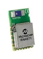


RN4871-I/RM130
Bluetooth 4.2, 1.9V to 3.6V Supply, RN4871 Series Range, 10Mbps, -90dBm Sensitivity
- Manufacturer: MICROCHIP
- Product type: Bluetooth Modules & Adaptors
- Bluetooth Version:Bluetooth 4.2; Supply Voltage Min:1.9V; Supply Voltage Max:3.6V; Signal Range Max:-; Data Rate:10Mbps; Bluetooth Class:-; Receive Sensitivity:-90dBm; Operating Tem
- SVHC: No SVHC (04-Feb-2026)
- Interfaces: I2C, SPI, UART
- Product Range: RN4871 Series
- Certifications: CE, FCC, ISED, KC, NCC, SRRC
- Bluetooth Class: -
- Bluetooth Version: Bluetooth 4.2
- Supply Voltage Range: 1.9 V to 3.6 V
- Receiver Sensitivity Rx: -90 dBm
- Operating Temperature Range: -40 °C to 85 °C
| Delivery and price | |
|---|---|
| Units per pack | 250 |
| Price | 6.38 € |
| Current stock | 500+ |
| Lead time | 30 days |
## **RN4870/71** ~~MICROCHIP~~ **Bluetooth[®] 4.2 Low Energy Module** ## **Features** - Fully Qualified Bluetooth[®] Low Energy Module - Certified to FCC, IC, CE, KCC, NCC and SRRC - On-Board Bluetooth 4.2 Low Energy Stack - ASCII Command Interface API over UART - Scripting Engine for Hostless Operation - Compact Form Factor – The RN4870/71 family comes in four different sizes from 6 mm x 8 mm to 12 mm x 22 mm: - RN4870: 12 mm x 22 mm - RN4871: 9 mm x 11.5 mm - RN4870U: 12 mm x 15 mm - RN4871U: 6 mm x 8 mm - Beacon Private Service for Beacon Services - UART Transparent Service for Serial Data Applications - Remote Configuration Over The Air ## **Operational** - Operating Voltage: 1.9V to 3.6V (3.3V typical) - Temperature Range: - -20°C to +70°C (Normal) - -40°C to +85°C (Industrial) - Supports UART - Up to Three Pulse Width Modulation (PWM) Outputs ## **Antenna Options** ## **RF/Analog Features** - ISM Band 2.402 to 2.480 GHz Operation - Channels: 0-39 - RX Sensitivity: -90 dBm - TX Power: 0 dBm - RSSI Monitor ## **MAC/Baseband/Higher Layer Features** - Secure AES128 Encryption - GAP, GATT, SM, L2CAP and Integrated Public Profiles - Customer Can Create up to Five Public and Four Private Services - Keyboard I/O Authentication - Software Configurable Role as Peripheral or Central and Client or Server - Integrated Chip Antenna (RN487x) - refer to **Section 8.0, Antenna Characteristics** , Figure 8-1 and Figure 8-2 for antenna performance specifications - External Antenna Connection via RF Pad (RN4870U/RN4871U) ## **Applications** - Health/Medical Devices - Sports Activity/Fitness Meters - Beacon Applications - Internet of Things (IoT) Sensor Tag - Remote Control - Wearable Smart Devices and Accessories - Smart Energy/Smart Home - Industrial Control DS50002489C-page 1 2016-2017 Microchip Technology Inc. **RN4870/71** ## **Table of Contents** |1.0|Device Overview .......................................................................................................................................................................... 3| |---|---| |2.0|Specifications ............................................................................................................................................................................... 9| |3.0|Interface PINs..............................................................................................................................................................................11| |4.0|Physical Dimensions And Attributes ........................................................................................................................................... 13| |5.0|Application Reference Circuits ................................................................................................................................................... 23| |6.0|ASCII Command API.................................................................................................................................................................. 29| |7.0|Supported Services .................................................................................................................................................................... 31| |8.0|Antenna Characteristics ............................................................................................................................................................. 33| |9.0|Timing Characteristics................................................................................................................................................................ 35| |10.0|Regulatory Approval ................................................................................................................................................................... 37| |11.0|Ordering Information .................................................................................................................................................................. 43| |The|Microchip Web Site ....................................................................................................................................................................... 45| |Customer Change Notification Service ................................................................................................................................................ 45|| |Customer Support................................................................................................................................................................................ 45|| |Product Identification System............................................................................................................................................................... 46|| ## **TO OUR VALUED CUSTOMERS** It is our intention to provide our valued customers with the best documentation possible to ensure successful use of your Microchip products. To this end, we will continue to improve our publications to better suit your needs. Our publications will be refined and enhanced as new volumes and updates are introduced. If you have any questions or comments regarding this publication, please contact the Marketing Communications Department via E-mail at **docerrors@microchip.com** . We welcome your feedback. ## **Most Current Data Sheet** To obtain the most up-to-date version of this data sheet, please register at our Worldwide Web site at: ## **http://www.microchip.com** You can determine the version of a data sheet by examining its literature number found on the bottom outside corner of any page. The last character of the literature number is the version number, (e.g., DS30000000A is version A of document DS30000000). ## **Errata** An errata sheet, describing minor operational differences from the data sheet and recommended workarounds, may exist for current devices. As device/documentation issues become known to us, we will publish an errata sheet. The errata will specify the revision of silicon and revision of document to which it applies. To determine if an errata sheet exists for a particular device, please check with one of the following: - Microchip’s Worldwide Web site; **http://www.microchip.com** - Your local Microchip sales office (see last page) When contacting a sales office, please specify which device, revision of silicon and data sheet (include literature number) you are using. ## **Customer Notification System** Register on our web site at **www.microchip.com** to receive the most current information on all of our products. DS50002489C-page 2 2016-2017 Microchip Technology Inc. **RN4870/71** ## **1.0 DEVICE OVERVIEW** ## **1.1 Overview** The RN4870/71 Bluetooth Low Energy (BLE) modules integrate Bluetooth 4.2 baseband controller, on-board Bluetooth stack, digital and analog I/O, and RF power amplifier into one solution. Table 1-1 shows the various options for packaging and features available in the RN4870/71 family. Table 1-2 provides the description of the pin functions for all the modules in the RN4870/71 family. Figure 1-1 through Figure 1-4 show the pinout for the different modules. **TABLE 1-1: RN4870/71 FAMILY** |**Part Number(1)**|**Antenna**<br>**On-Board**|**Shielding**|**Number of**<br>**Pins**|**Dimensions**|**Operating**<br>**Temperature Range**| |---|---|---|---|---|---| |RN4870-V/RMXXX|Yes|Yes|33|12 mm x 22 mm|-20°C to +70°C| |RN4870U-V/RMXXX|No|No|30|12 mm x 15 mm|-20°C to +70°C| |RN4871-V/RMXXX|Yes|Yes|16|9 mm x 11.5 mm|-20°C to +70°C| |RN4871U-V/RMXXX|No|No|17|6 mm x 8 mm|-20°C to +70°C| |RN4870-I/RMXXX|Yes|Yes|33|12 mm x 22 mm|-40°C to +85°C| |RN4871-I/RMXXX|Yes|Yes|16|9 mm x 11.5 mm|-40°C to +85°C| **Note 1:** The last three digits in P/N indicate the firmware version. At the time of publication, the latest firmware version is 1.28. Ensure to check product webpage for latest part number and firmware version. ## **TABLE 1-2: PIN DESCRIPTION** |**RN4870U **|**RN4870 **|**RN4871U **|**RN4871**|**Name**|**Type**|**Description**| |---|---|---|---|---|---|---| |—|1|—|—|GND|Power|Ground reference| |—|2|—|—|GND|Power|Ground reference| |1|3|12|13|GND|Power|Ground reference| |2|4|11|14|VBAT|Power|Positive supplyinput. Range: 1.9V~3.6V| |—|—|10|—|BK_IN|Power|Buck power supply input<br>Can be connected to the VBAT pin<br>Connect to 10 µF low ESR ceramic capacitor<br>Voltage range: 1.9V to 3.6V| |3|5|—|—|P2_2|D I/O|GPIO<br>PWM1<br>Default: Input;pulled-high| |4|6|—|—|VDD_IO|Power|VDD; power input<br>Same input pin as VBAT<br>Can be connected to the VBATpin| |5|7|—|—|VDD_IO|Power|VDD; power input<br>Same input pin as VBAT<br>Can be connected to the VBATpin| |6|8|—|—|ULPC_O|Power|1.2V ULPC LDO output<br>Used for diagnostic purposes<br>_Do not connect_to any pin or device<br>For measurement, connect a bypass 1 µF<br>capacitor toground| |7|9|—|—|P2_3|D I/O|GPIO<br>PWM2<br>Default: Input;pulled-high| |8|10|—|—|BK_O|Power|1.55V Buck power supply output for diagnostic<br>purpose<br>_Do not connect_| |—|—|13|6|P1_6|D|Configurable pin. Refer to**Section 1.2 “Module**<br>**Configuration”**for details.| DS50002489C-page 3 2016-2017 Microchip Technology Inc. ## **RN4870/71** **TABLE 1-2: PIN DESCRIPTION (CONTINUED)** |**RN4870U **|**RN4870 **|**RN4871U **|**RN4871**|**Name**|**Type**|**Description**| |---|---|---|---|---|---|---| |—|—|14|5|P1_7|D|Configurable pin. Refer to**Section 1.2 “Module**<br>**Configuration”**for details.| |9|11|15|15|P2_7|D O/p|UART_TX_IND output pin. Provides indication if<br>RN4870 is transmitting to host MCU over UART.<br>Pulled low before UART TX begins and pulled high<br>after UART TX is over.| |10|12|—|—|P1_1|D I/O<br>A I/p|GPIO; default: Input; pulled-high<br>AD9<br>Configured as the BLEDK_STATUS1_IND pin by<br>default| |11|13|2|3|P1_2|D I/O<br>A I/p|GPIO; default: Input; pulled-high<br>AD10; I2C SCLpin| |12|14|3|4|P1_3|D I/O|GPIO; default: Input; pulled-high<br>AD11; I2C SDApin| |13|15|8|11|P0_0|D I/O|GPIO; default: Input; pulled-high<br>AD0<br>Configured as the UART_CTSpin bydefault| |14|16|—|—|P1_0|D I/O|GPIO; default: Input; pulled-high<br>AD8<br>Configured as the BLEDK_STATUS2_IND pin by<br>default| |15|17|6|9|P3_6|D I/O|GPIO; default: Input; pulled-high<br>PWM0<br>Configured as the UART_RTSpin bydefault| |16|18|16|16|P2_0|D I/p|System configuration input;<br>1: Application mode<br>0: Test mode/Flash update/EEPROM configuration<br>Default: Input;pulled-high| |17|19|—|—|P2_4|D I/O|GPIO; default: Input;pulled-high| |18|20|—|—|NC|—|No Connection| |19|21|7|10|RST_N|D I/p|Module Reset; active-low; Internally pulled-high| |20|22|5|7|UART_RX|D I/p|UART Data input| |21|23|4|8|UART_TX|D O/p|UART Data output| |22|24|—|—|P3_1|D I/O|GPIO; default: Input; pulled-high<br>Configured as RSSI_IND pin by default; SPI NCS<br>Bus| |23|25|—|—|P3_2|D I/p|GPIO; default: Input; pulled-high<br>Configured as the LINK_DROP pin by default; SPI<br>MISOpin| |24|26|—|—|P3_3|D I/p|GPIO; default: Input; pulled-high<br>Configured as the UART RX Indication pin by default;<br>SPI MOSIpin| |25|27|—|—|P3_4|D I/p|GPIO; default: Input; pulled-high<br>Configured as the PAIRING_KEY pin by default; SPI<br>SCLKpin| |26|28|—|—|P3_5|D I/O<br>A I/p|GPIO; default: Input; pulled-high<br>LED1; provides indication whether the module is ON/<br>OFF| |27|29|—|—|P0_7|D I/O|GPIO; default: Input; pulled-high<br>Configured to the LOW_BATTERY_INDICATOR pin<br>bydefault| DS50002489C-page 4 2016-2017 Microchip Technology Inc. **RN4870/71** ## **TABLE 1-2: PIN DESCRIPTION (CONTINUED)** |**RN4870U **|**RN4870 **|**RN4871U **|**RN4871**|**Name**|**Type**|**Description**| |---|---|---|---|---|---|---| |28|30|9|12|P0_2|D I/O|AD2<br>LED0: Provides indication whether the module is in<br>ON/OFF mode| |29|31|17|2|GND|Power|Ground Reference| |—|32|—|—|GND|Power|Ground Reference| |30|—|1|—|BT_RF|A I/O|External Antenna connection (50 ohms). Only for<br>RN4870U and RN4871U. No connection for RN4871.| |—|33|—|—|GND|Power|Ground Reference| |**Legend:**<br>Pin Type Abbreviations: A = Analog D = Digital I/O = Input/Output I/p = Input O/p = Output||||||| **FIGURE 1-1: PIN DIAGRAM - RN4870U** **==> picture [468 x 493] intentionally omitted <==** **----- Start of picture text -----**<br> Top View Bottom View<br>GND 1 30 BT_RF 30 1<br>VBAT 2 TP-3 TP-3 VCC_RF<br>P2_2 3 29 GND TP-1 VCC_PA<br>VDD_IO 4 28 P0_2/LED TP-1<br>VDD_IO 5 27 P0_7<br>ULPC_O 6 26 P3_5<br>P2_3 7 25 P3_4<br>BK_O 8 24 P3_3<br>P2_7/TX_IND 9 23 P3_2 TP-2 TP-2 CLDO_O<br>P1_1 10 22 P3_1<br>P1_2 11 21 UART_TX<br>P1_3 12 20 UART_RX<br>FIGURE 1-2: PIN DIAGRAM - RN4870<br>Top View Bottom View<br>GND 1 33 GND 33 1<br>GND 2 32 GND<br>GND 3<br>VBAT 4 TP-3 TP-3 VCC_RF<br>P2_2 5 31 GND TP-1 VCC_PA<br>VDD_IO 6 30 P0_2/LED TP-1<br>VDD_IO 7 29 P0_7<br>ULPC_O 8 28 P3_5<br>P2_3 9 27 P3_4<br>BK_O 10 26 P3_3<br>P2_7/TX_IND 11 25 P3_2 TP-2 TP-2 CLDO_O<br>P1_1 12 24 P3_1<br>P1_2 13 23 UART_TX<br>P1_3 14 22 UART_RX<br>13 14 15 16 17 18 19<br>P0_0/CTS P1_0 P3_6/RTS P2_0/MODE P2_4 NC RST_N<br>15 16 17 18 19 20 21<br>P0_0/CTS P1_0 P3_6/RTS P2_0/MODE P2_4 NC RST_N<br>**----- End of picture text -----**<br> DS50002489C-page 5 2016-2017 Microchip Technology Inc. **RN4870/71** **FIGURE 1-3:** **PIN DIAGRAM - RN4871U** **==> picture [423 x 241] intentionally omitted <==** **----- Start of picture text -----**<br> Top View Bottom View<br>1<br>Po<br>UART_RX 5<br>P3_6 6 17 GND 17 == TP-1 L¢X< TP-1 CLDO_O<br>RST_N 7 16 P2_0 TP-2 TP-4<br>P0_0P0_2 89 &X 1514 P2_7P1_7 VCC_RF TP-2 VCC_PA TP-3 nmio TP-3 TP-5 =im TP-4 ULPC_OTP-5 BK_O<br>XX I IAI IN Ax<br>UART_TX P1_3 P1_2 BT_RF<br>4 3 2 1<br>10 11 12 13<br>BK_IN VBAT GND P1_6<br>**----- End of picture text -----**<br> **FIGURE 1-4:** **PIN DIAGRAM - RN4871** **==> picture [143 x 58] intentionally omitted <==** **----- Start of picture text -----**<br> 16 Yi<br>TP-3<br>o U =: 7p-a VEC PA<br>TP-2TP-4 Lixz“<(A, TP-2.. VCC_RF-<br>TP-1<br>TP-5 —_ TP-4 ULPC_O<br>**----- End of picture text -----**<br> DS50002489C-page 6 2016-2017 Microchip Technology Inc. **RN4870/71** ## **1.2 Module Configuration** The GPIO pins of the RN4870 and RN4871 modules can be configured to different functions using the ASCII command interface. Table 1-3 shows the various pins in the RN4870/71 module that are available for configuration and their default configuration settings. Table 1-4 provides details on each functions available. Table 1-5 shows the status of the module as indicated by the Status 1 and Status 2 indication pins. Table 1-6 shows the details of test pads that are present on the bottom side of the module, used for diagnostic purposes during testing. Figure 1-5 shows all the key elements of the module. **TABLE 1-3: CONFIGURABLE PINS AND DEFAULT FUNCTIONS IN THE RN4870 AND RN4871** |**Pin Name**|**Available in**|**Available in**|**Default Function**| |---|---|---|---| ||**RN4870**|**RN4871**|| |P0_7|x|—|Low BatteryIndication| |P1_0|x|—|Status 2| |P1_1|x|—|Status 1| |P2_2|x|—|None| |P2_4|x|—|None| |P3_1|x|—|RSSI Indication| |P3_2|x|—|Link Drop| |P3_3|x|—|UART RX Indication| |P3_4|x|—|PairingKey| |P3_5|x|—|None| |P1_2|x|x|None| |P1_3|x|x|None| |P1_6|—|x|UART RX Indication| |P1_7|—|x|None| ## **TABLE 1-4: CONFIGURABLE FUNCTIONS AND DESCRIPTIONS** |**Function Name**|**Description**| |---|---| |Low Battery Indication|Pin output goes low when the VDDis below a specified level. To set the<br>threshold level, change the EEPROM settings.| |Status 1|Use this indication pin along with the Status 2 pin to indicate the current status of<br>the module. Refer toTable 1-5for details of the status indication.| |Status 2|Use this indication pin along with the Status 1 pin to indicate the current status of<br>the module. Refer toTable 1-5for details of the status indication.| |RSSI Indication|Use this indication pin to indicate the quality of the link based on the RSSI level.<br>If the RSSI level is lower than the specified threshold value, then the RSSI<br>indicationpingoes low. Set the threshold for the RSSI linkqualityin EEPROM.| |Link Drop|When the RN4870/71 is connected to a remote device, the host MCU can use<br>the Link Drop pin to force the module to disconnect the link and and enter<br>shutdown state. Thepin needs to bepulled low for at least 10 ms.| |UART RX Indication|Use this pin to enable communication with the UART when the module is in Low-<br>Power mode. When_not_in Low-Power mode, the module runs on a 16 MHz<br>clock. If Low-Power mode is enabled on the module by using commandSO,1,<br>the module runs on a 32 kHz clock thus reducing power consumption. However,<br>in Low-Power mode, the host MCU_cannot_communicate with the module via the<br>UART since the UART is_not_operational. If the user intends to provide data or<br>commands via UART in the Low-Power mode, then the UART RX INDICATION<br>pin must be pulled low and the user needs to wait for at least five milliseconds<br>before sending the data. Pulling the UART RX INDICATION pin low allows the<br>module to operate the 16 MHz clock and to enable UART.| DS50002489C-page 7 2016-2017 Microchip Technology Inc. **RN4870/71** **TABLE 1-4: CONFIGURABLE FUNCTIONS AND DESCRIPTIONS (CONTINUED)** |**Function Name**|**Description**| |---|---| |Pairing Key|When the RN4870/71 is connected to a remote device, the host MCU can use<br>the Pairing Key pin to force the module to disconnect the link and go back to<br>standbystate. Thepin must bepulled down for at least 160 ms.| |RF Active Indication|Use this indication pin to indicate that the module is currently performing an<br>active transmission and receivingBLE data.| ## **TABLE 1-5: STATUS INDICATION PINS** |**Status 1**|**Status 2**|**State**| |---|---|---| |High|High|Power On| |High|Low|Standbystate| |Low|Low|Connection established| |Low|High|Data session open(Transparent UART)| ## **TABLE 1-6: TEST POINTS ON THE BOTTOM SIDE** |**RN4870U**|**RN4870**|**RN4871U**|**RN4871**|**Symbol**|**Description**| |---|---|---|---|---|---| |TP-1|TP-1|TP-3|TP-3|VCC_PA|1.55V RF PA LDO| |TP-2|TP-2|TP-1|TP-5|CLDO_O|1.2V CLDO Output| |TP-3|TP-3|TP-2|TP-2|VCC_RF|1.2V RF LDO Output| |—|—|TP-4|TP-4|ULPC_O|1.2V ULPC LDO Output| |—|—|TP-5|TP-1|BK_O|1.55V Buck RegOutput| ## **FIGURE 1-5: BLOCK DIAGRAM OF THE RN4870/71** **==> picture [70 x 8] intentionally omitted <==** **----- Start of picture text -----**<br> RN4870/RN4871<br>**----- End of picture text -----**<br> DS50002489C-page 8 2016-2017 Microchip Technology Inc. **RN4870/71** ## **2.0 SPECIFICATIONS** Table 2-1 provides the general specifications for the module. Table 2-2, Table 2-3 and Table 2-4 provide the electrical characteristics and the current consumption of the module. ## **TABLE 2-1: GENERAL SPECIFICATIONS** |**TABLE 2-1:**<br>**GENERAL SPECIFICATIONS**|| |---|---| |**Specification**|**Description**| |Standard Compliance|Bluetooth 4.2| |FrequencyBand|2.402 to 2.480 GHz| |Modulation Method|GFSK| |Maximum Data Rate(Transparent UART)|10 kbps(iOS®9)| |Antenna|Ceramic| |Interface|UART, AIO, PIO| |OperatingRange|1.9V to 3.6V| |Sensitivity|-90 dBm| |RF TX Power|0 dBm| |OperatingTemperature Range for RN4870-I and RN4871-I modules|-40°C to +85°C| |OperatingTemperature Range for RN4870-V and RN4871-V modules|-20°C to +70°C| |Storage Temperature Range|-40°C to +125°C| |OperatingRelative HumidityRange|10% to 90%| |Storage Relative HumidityRange|10% to 90%| |Moisture SensitivityLevel|2| ## **TABLE 2-2: ELECTRICAL CHARACTERISTICS** |**Parameter**|**Min.**|**Typ.**|**Max.**|**Units**| |---|---|---|---|---| |SupplyVoltage(VDD)|1.9|—|3.6|V| |**I/O Voltage Levels**||||| |VILInput Logic Levels Low|VSS|—|0.3 VDD|V| |VIHInput Logic Levels High|0.7 VDD|—|VDD|V| |VOLOutput Logic Levels Low|Vss|—|0.2 VDD|V| |VOHOutput Logic Levels High|0.8 VDD|—|VDD|V| |**Reset**||||| |Reset Low Duration|63|—|—|ns| |**Input and Tri-State Current with**||||| |Pull-UpResistance|34|48|74|k| |Pull-Down Resistance|29|47|86|k| DS50002489C-page 9 2016-2017 Microchip Technology Inc. ## **RN4870/71** ## **TABLE 2-3: CURRENT CONSUMPTION** |**TABLE 2-3:**<br>**CURRENT CONSUMPTION**||||| |---|---|---|---|---| |**Parameter**|**Min.**|**Typ.**|**Max.**|**Units**| |**Supply Current**||||| |TX mode Peak Current at VDD= 3V, TX = 0 dBm, Buck mode|—|10 at +25°C|13 at +75°C/+85°C|mA| |RX mode Peak Current at VDD= 3V, Buck mode|—|10 at +25°C|13 at +75°C/+85°C|mA| |Low-Power Mode Current**(2)**|—|60 at +25°C|—|µA| |Shutdown Low-Power Mode|1|—|2.9|µA| - **Note 1:** The current measurements are characterized across a sample of RN4870/71 modules at room temperature (+25°C), unless otherwise noted. - **2:** For more details on Low-Power mode, refer to the “ _RN4870/71 Bluetooth[®] Low Energy Module User’s Guide”_ (DS50002466). ## **TABLE 2-4: CURRENT CONSUMPTION DURING APPLICATION MODE** |**Test Mode**|**Interval**<br>**(ms)**|**Average Current Consumption**| |---|---|---| |Advertising**(1,2,3)**|20|1.061 mA| ||50|505µA| ||100|298µA| ||500|113µA| ||1000|89µA| |Connected**(1,2,4)**|18.75|2.23 mA| ||50|2.13 mA| ||100|2.10 mA| ||500|83µA| ||1000|80µA| **Note 1:** These measurements are done at an operating temperature of +25°C at 3.3V and are characterized across a sample of RN4870/71 modules. - **2:** Measurements taken with version 1.18 firmware loaded onto the module. - **3:** The advertising packet data payload is approximately 15 bytes in length. - **4:** The amount of data being transmitted between two peer devices can affect the average current measured. The average current measurements are done with only the necessary Bluetooth packets being exchanged to keep the connection active at the stated interval. DS50002489C-page 10 2016-2017 Microchip Technology Inc. **RN4870/71** ## **3.0 INTERFACE PINS** Figure 3-1 shows the power scheme using a 3.3V low-dropout regulator to the RN487x and a host MCU. This scheme ensures that the same voltage is used for both the module and the MCU. Figure 3-1 also shows the basic UART connections to the host MCU. Figure 3-2 shows the recommended connections for running the RN4870/71 on coin cell battery. ## **FIGURE 3-1:** ## **POWER SCHEME** **==> picture [444 x 500] intentionally omitted <==** **----- Start of picture text -----**<br> RN4870/71/70U<br>VBAT a<br>(19-36) TxD Rx Note 1<br>ResRes e t ICt IC Reset<br>a “yp<br>Control &<br>— indication UOs(S—] “O#<br>Note 2, Note 3<br>D PO_2LED<br>pa!<br>&<br>Note 1: Ensure VDD_IO and MCU VDD voltages are compatible<br>System Configurator<br>2: Control and Indication ports are configurable<br>3: To implement low-power operation, enable the UART_RX_IND<br>pin and connect to ground.<br>vin (3.3V)<br>LDO<br>RN4871U<br>ene em - vDD<br>Note 3—E ¢ TXD RX Net<br>BK_IN Note 4 ee ay<br>Reset IC Reset<br>Control &<br>— NoteIndication2, NoteVOs|S—]5 “OS<br>aa PO_2LED<br>Note 3 °,<br>System Configurator Note 1: Ensure VDD_IO and MCU VDD voltages are compatible<br>2: Control and Indication ports are configurable<br>3: 10 µF (X5R) and 330 ohm resistor are required for RN487x<br>4: BK_IN connects to VBAT for RN4871U<br>5: To implement low-power operation, enable the UART_RX_IND<br>pin and connect to ground.<br>**----- End of picture text -----**<br> DS50002489C-page 11 2016-2017 Microchip Technology Inc. ## **RN4870/71** ## **FIGURE 3-2: RN4870/71 COIN CELL POWER SCHEME** **==> picture [174 x 122] intentionally omitted <==** **----- Start of picture text -----**<br> RN4870/71<br>Cell<br>; BAT_IN<br>| (1.9~3.6V)<br>BK_IN<br>Note 2<br>Reset IC Reset<br>las<br>**----- End of picture text -----**<br> - **Note 1:** Application includes ADC, PWM (RN4870), and I[2] C bus interface - **2:** BK_IN connection is needed only for RN4871U. **3:** To implement low-power operation, enable the UART_RX_IND pin and connect to ground. The Configuration pins on the RN4870 can also be configured through Windows[®] -based User Interface (UI) Configuration tool, BLEDK3. DS50002489C-page 12 2016-2017 Microchip Technology Inc. **RN4870/71** ## **4.0 PHYSICAL DIMENSIONS AND ATTRIBUTES** ## **4.1 RN4870 Module** Figure 4-1 shows the physical dimensions of the RN4870 module. Figure 4-2 illustrates the recommended PCB layout, and Figure 4-3 shows the recommended mounting details. Ensure that there is _no_ top copper layer near the test pin area, indicated by the shaded _keep out areas_ , as shown in Figure 4-2. When laying out the host PCB, the areas under the antenna must _not_ contain any top, inner layer, or bottom copper as shown in Figure 4-3. A low-impedance ground plane ensures the best radio performance (best range; lowest noise). Figure 4-3 also shows a minimum ground plane area to the left and right side of the module for best antenna performance. The ground plane can be extended beyond the minimum recommended as required for host PCB EMC noise reduction. For best range performance, keep all external metal at least 30 mm away from the ceramic chip antenna. ## **FIGURE 4-1: RN4870 MODULE DIMENSIONS** DS50002489C-page 13 2016-2017 Microchip Technology Inc. **RN4870/71** **FIGURE 4-2: RN4870 RECOMMENDED PCB FOOTPRINT** **FIGURE 4-3: RECOMMENDED MOUNTING DETAILS** DS50002489C-page 14 2016-2017 Microchip Technology Inc. **RN4870/71** ## **4.2 RN4870U Module** Figure 4-4 shows the physical dimensions of the RN4870U module. Figure 4-5 illustrates the recommended PCB layout, and Figure 4-6 shows the recommended mounting details. A low-impedance ground plane ensures the best radio performance (best range; lowest noise). Pin 30 (BT_RF) is a 50 ohm connection that can be connected ## **FIGURE 4-4:** ## **RN4870U MODULE DIMENSIONS** to an external antenna such as a PCB trace antenna, a component (chip) antenna, or through a host PCB 50 ohm microstrip trace. This trace can be extended to include passive parts for antenna attenuation padding, impedance matching, or to provide test posts. It is recommended that the microstrip trace to be as short as possible for minimum loss and best impedance matching. If the microstrip trace is longer, a 50 ohm impedance is recommended. DS50002489C-page 15 2016-2017 Microchip Technology Inc. **RN4870/71** **FIGURE 4-5: RN4870U RECOMMENDED PCB FOOTPRINT** **FIGURE 4-6: RN4870U RECOMMENDED PCB MOUNTING** DS50002489C-page 16 2016-2017 Microchip Technology Inc. **RN4870/71** ## **4.3 RN4871 Module** Figure 4-7 shows the physical dimensions of the RN4871 module. Figure 4-8 illustrates the recommended PCB layout, and Figure 4-9 shows the recommended mounting details. Ensure that there is _no_ top copper layer near the test pin area, indicated by the shaded _keep out areas_ , as shown in Figure 4-8. When laying out the host PCB, the areas under the antenna must _not_ contain any top, inner layer, or bottom copper as shown in Figure 4-9. A low-impedance ground plane ensures the best radio performance (best range; lowest noise). Figure 4-9 also shows a space area around antenna section for best antenna performance. The ground plane can be extended beyond the minimum recommended as required for host PCB EMC noise reduction. For best range performance, keep all external metal at least 30 mm away from the ceramic chip antenna. ## **FIGURE 4-7: RN4871 MODULE DIMENSIONS** **==> picture [460 x 260] intentionally omitted <==** **----- Start of picture text -----**<br> Top View Side View Bottom View<br>11.5 11.14 11.5<br>Shield<br>9.54 mounting hole<br>7.5 7.18 7.5<br>6.7 1 16 6.7 16 6.7<br>TP-3 6.01 TP-3<br>5.5 5.5<br>4.33.1 4.33.1 TP-1 TP-2TP-4 4.114.853.68 TP-1 TP-2TP-4 4.75<br>TP-5 1.2 2.38 TP-5<br>1.9 Shield 1.9<br>0.70 mounting<br>0.0 0.00 hole 0.0 0.0<br>Shield<br>mounting hole<br>Pad Positions Test Point Positions<br>1.0<br>Dimensions are in millimeters<br>Tolerances: 0.7 0.5 0.7<br>PCB Thikness: +/-0.06mm<br>Pad Detail<br>0.58 8.31 5.79 5.33 0.63<br>0.0 1.5 2.7 3.9 5.1 6.3 7.5 9.0 2.1 0.6 0.0 9.0 7.5 6.3 5.1 3.9 2.7 1.5 0.0<br>6.93 6.0 5.25 0.0<br>**----- End of picture text -----**<br> DS50002489C-page 17 2016-2017 Microchip Technology Inc. **RN4870/71** ## **FIGURE 4-8: RN4871 RECOMMENDED PCB FOOTPRINT** **==> picture [246 x 285] intentionally omitted <==** **----- Start of picture text -----**<br> Top View<br>11.5 tt<br>Keep Out Area 0.5<br>1.5<br>7.5<br>7.0<br>6.7<br>5.5 0.7<br>4.6<br>4.3<br>=<br>3.1<br>1.2<br>1.9<br>== UE: 1.5<br>0.0 Keep Out Area<br>~ooo00r<br>Dimensions are in millimeters<br>1.0 3.0 4.3 8.0<br>0.0 1.5 2.7 3.9 5.1 6.3 7.5 9.0<br>**----- End of picture text -----**<br> **FIGURE 4-9: RN4871 RECOMMENDED PCB MOUNTING SUGGESTION** DS50002489C-page 18 2016-2017 Microchip Technology Inc. **RN4870/71** ## **4.4 RN4871U Module** Figure 4-10 shows the physical dimensions of the RN4871U module. Figure 4-11 illustrates the recommended PCB layout. It is highly recommended to layout the host PCB as suggested in Figure 4-12. Figure 4-13 shows the recommended placement for the module on the host PCB board. For optimal transmission and reception sensitivity, place the module at the edge of the board. A low-impedance ground plane ensures the best radio performance (best range; lowest noise). Pin 1 (BT_RF) is a 50 ohm connection that can be connected to an external antenna such as a PCB trace antenna, a component (chip) antenna, or through a host PCB 50 ohm microstrip trace. This trace can be extended to include passive parts for antenna attenuation padding, impedance matching, or to provide test posts. It is recommended that the microstrip trace to be as short as possible for minimum loss and best impedance matching. If the microstrip trace is longer, a 50 ohm impedance is recommended. ## **FIGURE 4-10: RN4871U MODULE DIMENSIONS** **==> picture [306 x 10] intentionally omitted <==** **----- Start of picture text -----**<br> Top View Side View Bottom View<br>**----- End of picture text -----**<br> DS50002489C-page 19 2016-2017 Microchip Technology Inc. **RN4870/71** **FIGURE 4-11: RN4871U RECOMMENDED PCB FOOTPRINT** **FIGURE 4-12: RN4871U RECOMMENDED PCB MOUNTING** DS50002489C-page 20 2016-2017 Microchip Technology Inc. **RN4870/71** ## **FIGURE 4-13: RECOMMENDATIONS FOR THE PLACEMENT OF THE MODULE ON THE HOST PCB BOARD** **==> picture [435 x 232] intentionally omitted <==** **----- Start of picture text -----**<br> Best<br>Acceptable<br>eSeeding ANT KeepOut Area<br>es —<br>\— 1 \——ima<br>‘y<br>i Acceptable<br>q<br>|4 i : |_|3<br>Em<br>——<br>c|<br>q<br>CI<br>Lowest<br>4<br>performance<br>**----- End of picture text -----**<br> ## **4.5 Soldering Recommendations** The RN4870/71 Bluetooth modules are assembled using standard lead-free reflow profile IPC/JEDEC J-STD-020. The module can be soldered to the host PCB using standard leaded and lead-free solder reflow profiles. To avoid damaging the module, the following recommendations are given: - Microchip Technology Application Note, _“AN233 Solder Reflow Recommendation”_ (DS00233) provides solder reflow recommendations - Do _not_ exceed peak temperature (TP) of 250°C - Refer to the solder paste data sheet for specific reflow profile recommendations - Use no-clean flux solder paste - Do _not_ wash as moisture can be trapped under the shield - Use only one flow. If the PCB requires multiple flows, apply the module on the final flow. DS50002489C-page 21 2016-2017 Microchip Technology Inc. **RN4870/71** ## **NOTES:** DS50002489C-page 22 2016-2017 Microchip Technology Inc. **RN4870/71** ## **5.0 APPLICATION REFERENCE CIRCUITS** ## **5.1 External Configuration and Programming** The RN4870/71 modules can be configured and firmware programmed using an external configuration and programming tool. Figure 5-1 shows the mandatory connections required between the module and the external programming header. It is recommended to include these pin connections on the host PCB for development. For accessing the various configuration and indication pins, use Table 1-2, Table 1-3, Table 1-4 and Table 1-5. ## **5.2 Reference Circuit** Figure 5-2 through Figure 5-5 show the reference circuits for various modules under the RN4870/71 family. In the circuits, the power input range is 1.9V ~ 3.6V. A battery reverse protection circuit is recommended in case a battery power input is used. Note that the VDD_IO is the same as the power input. In case of a LED connection, the power input must be greater than 3.0V. For the RN4870U, an RF antenna matching circuit must also be included as shown in Figure 5-3. ## **FIGURE 5-1: EXTERNAL PROGRAMMING HEADER CONFIGURATIONS** **==> picture [226 x 204] intentionally omitted <==** **----- Start of picture text -----**<br> RN4870/71<br>1 P2_0 P2_0<br>1 VBAT VBAT<br>1 RXD RXD<br>1 TXD TXD<br>1 GND GND<br>**----- End of picture text -----**<br> DS50002489C-page 23 2016-2017 Microchip Technology Inc. ## **FIGURE 5-2:** ## **RN4870 REFERENCE CIRCUIT** **==> picture [640 x 363] intentionally omitted <==** **----- Start of picture text -----**<br> 1 GND GND [33]<br>Reverse Voltage Protection 2 GND GND [32]<br>Power Input<br>Q1 GND<br>J1 STS2301 VCC GND 3 LED Option<br>GND<br>1 4 VCC<br>VBAT<br>2 P2_2 5 LD1<br>C1 6 P2_2 U1 GND [31] P0_2 P0_2 R1<br>VDD_IO P0_2 [30]<br>7 VDD_IO RN4870 P0_7 [29] P0_7 330<br>8 P3_5<br>ULPC_O P3_5 [28]<br>P2_3 9 P3_4<br>P2_3 P3_4 [27]<br>GND GND GND 10 P3_3<br>BK_O P3_3 [26]<br>10uF 6.3V X5R P2_7 11 P2_7/TX_IND P3_2 [25] P3_2 Configurable I/O<br>P1_1 12 P3_1 P0_0 P2_4<br>P1_1 P3_1 [24]<br>P1_2 13 UART_TX P0_7 P2_7<br>P1_2/SCL UART_TX [23]<br>P1_3 14 UART_RX P1_0 P3_1<br>P1_3/SDA UART_RX [22]<br>Configuration Interface UART Interface P1_1 P3_2<br>P2_0 VCC P1_2 P3_3<br>J2 P1_3 P3_4<br>1 VCC P2_2 P3_5<br>R2<br>2 P2_3 P3_6<br>4.7k<br>3 UART_RX RST<br>4 UART_TX<br>5 P2_0 MODE C2<br>1uF<br>Low Test Mode<br>GND<br>High APP Mode<br>GND<br>1 3<br>B<br>2<br>/CTS /RTS /MODE<br>_0 _0 _6 _0 _4<br>P0 P1 P3 P2 P2 NC RST<br>15 16 17 18 19 20 21<br>P0_0 P1_0 P3_6 P2_0 P2_4<br>**----- End of picture text -----**<br> ## **FIGURE 5-3:** ## **RN4870U REFERENCE CIRCUIT** **==> picture [637 x 344] intentionally omitted <==** **----- Start of picture text -----**<br> ANT1<br>Antenna Matching<br>Reverse Voltage Protection<br>L1<br>Power Input<br>Q1 1nH<br>J1 STS2301 VCC GND 1 GND BT_RF [30] C3 C4<br>1 2<br>VBAT<br>2 P2_2 3<br>C1 4 P2_2 U1 GND [29] P0_2<br>VDD_IO P0_2 [28]<br>5 RN4870U P0_7 GND GND<br>VDD_IO P0_7 [27]<br>6 P3_5<br>ULPC_O P3_5 [26]<br>P2_3 7 P3_4<br>P2_3 P3_4 [25]<br>GND GND GND 8 BK_O P3_3 [24] P3_3 LED Option<br>10uF 6.3V X5R P2_7 9 P3_2 VCC<br>P2_7/TX_IND P3_2 [23]<br>P1_1 10 P3_1 LD1<br>P1_1 P3_1 [22] R1<br>P1_2 11 UART_TX P0_2<br>P1_2/SCL UART_TX [21]<br>P1_3 12 P1_3/SDA UART_RX [20] UART_RX 330<br>Configuration Interface UART Interface<br>P2_0 VCC<br>J2 Configurable I/O<br>1 VCC P0_0 P2_4<br>R2<br>2 4.7k P0_7 P2_7<br>3 UART_RX RST P1_0 P3_1<br>4 UART_TX P1_1 P3_2<br>5 P2_0 MODE C2 P1_2 P3_3<br>1uF<br>P1_3 P3_4<br>Low Test Mode<br>P2_2 P3_5<br>GND P2_3 P3_6<br>High APP Mode<br>GND<br>1 3<br>2<br>B<br>/CTS /RTS /MODE<br>_0 _0 _6 _0 _4<br>P0 P1 P3 P2 P2 NC RST<br>13 14 15 16 17 18 19<br>P0_0 P1_0 P3_6 P2_0 P2_4<br>**----- End of picture text -----**<br> ## **FIGURE 5-4:** ## **RN4871 REFERENCE CIRCUIT** **==> picture [638 x 313] intentionally omitted <==** **----- Start of picture text -----**<br> Configuration Interface<br>P2_0 U1<br>J2 RN4871 Reverse Voltage Protection<br>1 VCC<br>2 1 NC P2_0 [16] P2_0 Q1 Power Input<br>3 UART_RX 2 GND P2_7 [15] P2_7 VCC STS2301 J1<br>4 UART_TX P1_3 3 P1_2 VBAT [14] 1<br>5 GND P1_2P1_7 45 P1_3P1_7 GNDP0_2 [13][12] P0_2 C1 2<br>GND GND<br>UART Interface<br>GND GND GND<br>VCC 10uF 6.3V X5R<br>Configurable I/O<br>R2<br>P0_0 P1_7 4.7k LED Option P2_0 MODE<br>P0_2 P2_0 RST VCC<br>P1_2 P2_7 LD1<br>R1 Low Test Mode<br>P1_3 P3_6 C2 Reset Circuit P0_2<br>1uF<br>P1_6 330 High APP Mode<br>GND<br>3 1<br>P1_6 UART_RX UART_TX P3_6 RST P0_0 2<br>6 7 8 9 10 11<br>1_6 ART_RX ART_TX<br>P U U P3_6 P0_0<br>B<br>**----- End of picture text -----**<br> ## **FIGURE 5-5:** ## **RN4871U REFERENCE CIRCUIT** **==> picture [640 x 345] intentionally omitted <==** **----- Start of picture text -----**<br> VCC LED Option VCC P2_0 MODE Configuration Interface<br>P2_0<br>LD1 J2<br>R1 R2 Low Test Mode<br>P0_2 VCC 1<br>4.7k<br>2<br>330 High APP Mode<br>RST UART_RX 3<br>Reverse Voltage Protection UART_TX 4<br>Power Input C2 5<br>Q1 1uF UART_RX<br>J1 STS2301 VCC UART_TX<br>1 UART Interface GND<br>2 GND<br>C1 10 BK_I UART_TX [4]<br>1112 VBATGND U1RN4871U P1_3P1_2 [3][2] P1_3P1_2<br>13 P1_6 BT_RF [1]<br>GND GND GND ANT1<br>10uF 6.3V X5R Antenna Matching<br>GND<br>L1<br>Configurable I/O P1_6 1nH<br>P0_0 P1_7 C3 C4<br>P0_2 P2_0<br>P1_2 P2_7<br>P1_3 P3_6 GND<br>P1_6 GND GND<br>B P0_2 P0_0 P3_6<br>9 8 7 6 5<br>1 3 P0_2 P0_0 RST P3_6<br>UART_RX<br>2<br>P1_7 P2_7 P2_0 GND<br>14 15 16 17<br>P1_7 P2_7 P2_0<br>**----- End of picture text -----**<br> ## **RN4870/71** ## **5.3 Power Drop Protection** To prevent any problems that may arise when the power supply goes below 1.9V, a power-supply dropprotection circuit is recommended. Essentially, this circuit consists of a Reset IC which acts as an _Open_ _Drain_ with a Delay =< 10 ms, and is triggered at 1.8V power supply. Figure 5-6 shows a recommended power drop protection circuit. ## **FIGURE 5-6: POWER DROP PROTECTION CIRCUIT** **==> picture [292 x 202] intentionally omitted <==** **----- Start of picture text -----**<br> VBAT<br>RN4870/71 Reset IC<br>RST_N OUT VDD<br>**----- End of picture text -----**<br> DS50002489C-page 28 2016-2017 Microchip Technology Inc. **RN4870/71** ## **6.0 ASCII COMMAND API** The RN4870/71 command Application Programming Interfaces (APIs) are documented in the _“RN4870/71 Bluetooth[®] Low Energy Module User's Guide”_ (DS50002466). The following are the available command options and their categories: - Connection - Establish connection - Disconnect - Bond/Unbond current connection - Start/Stop scan for other devices - Add/Delete peer devices to white list - Read RSSI values - Stop connection process - I/O - Read/Write I[2] C - Change settings in the EEPROM - Configure pin functions - Configure GPIO mask - Set/Get GPIO states - Read and write analog data - PWM control - GATT Services - Create/Delete public services/characteristics - Read/Write characteristic values - Set notification for characteristics - GAP Role - Central, Peripheral, Observer and Broadcaster - Advertising - Start/Stop - Set custom advertisement content - Set scan response content - Set beacon content - Private Service - Create/Delete private services/characteristics - Read/Write characteristic values - Set notification for characteristics - Transparent UART - Enable/Disable - Peripheral side configuration - Central side configuration - Remote configuration of the module - Read individual device Information or Profile settings - System - Reboot - Factory default - Enter and Exit Command mode - Enter Low-Power mode - Scripting - Enter Script mode - Declare event handler - Execute current script - List current script - Clear script - Define user function DS50002489C-page 29 2016-2017 Microchip Technology Inc. **RN4870/71** ## **NOTES:** DS50002489C-page 30 2016-2017 Microchip Technology Inc. **RN4870/71** ## **7.0 SUPPORTED SERVICES** The RN4870 supports four built-in GATT services: - Device Information public service - Airpatch private service, which handles Over The Air (OTA) updates - BeaconThings, which handles beacon services control - UART Transparent private service, which handles data streaming function In addition to the above predefined private services, the RN4870 provides the ability to create private services. If the services are supported on both end points of a Bluetooth Low Energy connection, such as Central and Peripheral devices, data can be exchanged. For example, two RN4870 modules can define a custom (private) service with its own unique characteristics. Data can be exchanged easily via Command API. Private services are _not_ registered with the Bluetooth SIG, and therefore _not_ interoperable with other Bluetooth Low Energy devices, unless the device implements the private service. An example of a builtin private service is the Transparent UART. For an example on how to create a custom service using the RN4870, refer to _“RN4870/71 Bluetooth[®] Low Energy Module User's Guide”_ (DS50002466). RN4870 allows custom defined services up to five public and four private services. Each custom defined service allows up to eight custom defined characteristics. All service definitions are saved in on-board Non-Volatile Memory (NVM) where the user must setup the module only once. DS50002489C-page 31 2016-2017 Microchip Technology Inc. **RN4870/71** ## **NOTES:** DS50002489C-page 32 2016-2017 Microchip Technology Inc. **RN4870/71** ## **8.0 ANTENNA CHARACTERISTICS** The RN4870 and RN4871 modules contain an integral ceramic chip antenna. Figure 8-1 and Figure 8-2 show the antenna performance on the modules. ## **FIGURE 8-1: RN4870 ANTENNA PERFORMANCE** |**Parameter**|||**Values**| |---|---|---|---| |Frequency|||2450 MHz| |Max Gain|||1.63 dBi| |Efficiency|||71.55%| ||||| |**Antenna Description**|**Manufacturer Part Number**||**Manufacturer**| |ANT ANT3216A063R2400A<br>PIFA 2.4GHz L3 2W1.6|ANT3216A063R2400A||Yageo| DS50002489C-page 33 2016-2017 Microchip Technology Inc. **RN4870/71** ## **FIGURE 8-2: RN4871 ANTENNA PERFORMANCE** |**Parameter**|||**Values**| |---|---|---|---| |Frequency|||2442 MHz| |Max Gain|||0.1 dBi| |Efficiency|||42.7%| ||||| |**Antenna Description**|**Manufacturer Part Number**||**Manufacturer**| |ANT AANT3216LL00R2400A<br>PIFA 2.4GHz L3 2W1.6|ANT3216LL00R2400A||Yageo| DS50002489C-page 34 2016-2017 Microchip Technology Inc. **RN4870/71** ## **9.0 TIMING CHARACTERISTICS** Figure 9-1 shows the timing diagram for the RN4870/ 71 modules when it is Reset in the Test mode and Application mode. Figure 9-2 shows the timing diagram for the module when it is powered on. In Application mode, when RN4870/71 is ready to talk to MCU after Reset, the module provides a UART response indicating that the Reset is complete. For more details, refer to the _“RN4870/71 Bluetooth[®] Low Energy Module User's Guide”_ (DS50002466). **FIGURE 9-1: TIMING DIAGRAM OF RN4870/71 UART READY AFTER RESET (IN TEST AND APPLICATION MODE)** **==> picture [340 x 204] intentionally omitted <==** **----- Start of picture text -----**<br> Ext<br>Reset ise<br>UART Ready<br>1mS for MCU<br>Test Mode<br>Process<br>P2_0=0<br>UART Ready<br>for MCU<br>Application<br>Mode<br>Process Status pin/UART<br>P2_0=1<br>Report Command<br>25mS<br>46mS<br>68mS<br>**----- End of picture text -----**<br> **FIGURE 9-2: TIMING DIAGRAM OF RN4870/71 UART WHEN POWERED ON (IN TEST AND APPLICATION MODE)** **==> picture [367 x 174] intentionally omitted <==** **----- Start of picture text -----**<br> VBAT a<br>UART Ready<br>for MCU<br>Test Mode P2_0=0<br>Process<br>25mS UART Ready<br>for MCU<br>Status pin/UART<br>Application P2_0=1<br>Mode Report Command<br>Process<br>46mS<br>68mS<br>**----- End of picture text -----**<br> DS50002489C-page 35 2016-2017 Microchip Technology Inc. ## **RN4870/71** Table 9-1 shows the error rate for various UART baud rates for the RN4870/71 module. The system clock is running at 16 MHz. ## **TABLE 9-1: ERROR RATE FOR VARIOUS BAUD RATES ON THE RN4870/71** |**Set Baud Rate**|**Measured Baud Rate**|**Error**| |---|---|---| |921600|941176|-2.12%| |460800|457143|0.79%| |307200|307692|-0.16%| |230400|231884|-0.64%| |115200|115942|-0.64%| |57600|57971|-0.64%| |38400|38095|0.79%| |19200|19048|0.79%| |9600|9524|0.79%| DS50002489C-page 36 2016-2017 Microchip Technology Inc. **RN4870/71** ## **10.0 REGULATORY APPROVAL** This section outlines the regulatory information for the RN4870/71 module for the following countries: - United States - Canada - Europe - Japan - Korea - Taiwan - China - Other Regulatory Jurisdictions ## **10.1 United States** The RN4870/71 module has received Federal Communications Commission (FCC) CFR47 Telecommunications, Part 15 Subpart C “Intentional Radiators” singlemodular approval in accordance with Part 15.212 Modular Transmitter approval. Single-modular transmitter approval is defined as a complete RF transmission sub-assembly, designed to be incorporated into another device, that must demonstrate compliance with FCC rules and policies independent of any host. A transmitter with a modular grant can be installed in different end-use products (referred to as a host, host product, or host device) by the grantee or other equipment manufacturer, then the host product may not require additional testing or equipment authorization for the transmitter function provided by that specific module or limited module device. A host product itself is required to comply with all other applicable FCC equipment authorization regulations, requirements, and equipment functions that are not associated with the transmitter module portion. For example, compliance must be demonstrated: to regulations for other transmitter components within a host product; to requirements for unintentional radiators (Part 15 Subpart B), such as digital devices, computer peripherals, radio receivers, etc.; and to additional authorization requirements for the non-transmitter functions on the transmitter module (i.e., Verification or Declaration of Conformity) as appropriate (e.g., Bluetooth and Wi-Fi transmitter modules may also contain digital logic functions). ## For the RN4870 module: Contains Transmitter Module FCC ID: A8TBM70ABCDEFGH _or_ Contains FCC ID: A8TBM70ABCDEFGH This device complies with Part 15 of the FCC Rules. Operation is subject to the following two conditions: (1) this device may not cause harmful interference, and (2) this device must accept any interference received, including interference that may cause undesired operation. Due to the limited size of the RN4871, the FCC Identifier (FCC ID) is not displayed on the module. Therefore, the FCC ID must be placed on the outside of the finished product into which the module is installed must also display a label referring to the enclosed module. This exterior label can use wording as follows: For the RN4871 module: Contains Transmitter Module FCC ID: A8TBM71S2 ## _or_ Contains FCC ID: A8TBM71S2 This device complies with Part 15 of the FCC Rules. Operation is subject to the following two conditions: (1) this device may not cause harmful interference, and (2) this device must accept any interference received, including interference that may cause undesired operation. ## 10.1.1 LABELING AND USER INFORMATION REQUIREMENTS The RN4870 module has been labeled with its own FCC ID number, and if the FCC ID is not visible when the module is installed inside another device, then the outside of the finished product into which the module is installed must also display a label referring to the enclosed module. This exterior label can use wording as follows: DS50002489C-page 37 2016-2017 Microchip Technology Inc. ## **RN4870/71** A user’s manual for the product should include the following statement: This equipment has been tested and found to comply with the limits for a Class B digital device, pursuant to part 15 of the FCC Rules. These limits are designed to provide reasonable protection against harmful interference in a residential installation. This equipment generates, uses and can radiate radio frequency energy, and if not installed and used in accordance with the instructions, may cause harmful interference to radio communications. However, there is no guarantee that interference will not occur in a particular installation. If this equipment does cause harmful interference to radio or television reception, which can be determined by turning the equipment off and on, the user is encouraged to try to correct the interference by one or more of the following measures: - Reorient or relocate the receiving antenna. - Increase the separation between the equipment and receiver. - Connect the equipment into an outlet on a circuit different from that to which the receiver is connected. - Consult the dealer or an experienced radio/TV technician for help. Additional information on labeling and user information requirements for Part 15 devices can be found in KDB Publication 784748 available at the FCC Office of Engineering and Technology (OET) Laboratory Division Knowledge Database (KDB) http://apps.fcc.gov/oetcf/kdb/index.cfm. ## 10.1.2 RF EXPOSURE All transmitters regulated by FCC must comply with RF exposure requirements. KDB Publication 447498 General RF Exposure Guidance provides guidance in determining whether proposed or existing transmitting facilities, operations or devices comply with limits for human exposure to Radio Frequency (RF) fields adopted by the Federal Communications Commission (FCC). FCC Office of Engineering and Technology (OET) Laboratory Division Knowledge Database (KDB): http://apps.fcc.gov/oetcf/kdb/index.cfm ## **10.2 Canada** The RN4870/71 module has been certified for use in Canada under Industry Canada (IC) Radio Standards Procedure (RSP) RSP-100, Radio Standards Specification (RSS) RSS-Gen, RSS-210, and RSS247. Modular approval permits the installation of a module in a host device without the need to recertify the device. ## 10.2.1 LABELING AND USER INFORMATION REQUIREMENTS Labeling Requirements (from RSP-100 - Issue 10, Section 3): The host device shall be properly labeled to identify the module within the host device. Modular Devices (from RSP-100 - Issue 10, Section 7): The Industry Canada certification label of a module shall be clearly visible at all times when installed in the host device, otherwise the host device must be labeled to display the Industry Canada certification number of the module, preceded by the words “Contains transmitter module”, or the word “Contains”, or similar wording expressing the same meaning, as follows: For the RN4870 module: Contains transmitter module IC: 12246A-BM70BLES1F2 Due to the limited size of the RN4871, the Industry Canada certification number is not displayed on the module. Therefore, the host device must be labeled to display the Industry Canada certification number of the module, preceded by the words “Contains transmitter module”, or the word “Contains”, or similar wording expressing the same meaning, as follows: Contains transmitter module IC: 12246A-BM71S2 Output power listed is conducted. This grant is valid only when the module is sold to OEM integrators and must be installed by the OEM or OEM integrators. This transmitter is restricted for use with the specific antenna(s) tested in this application for Certification and must not be co-located or operating in conjunction with any other antenna or transmitters within a host device, except in accordance with FCC multi-transmitter product procedures. This module is approved for installation into mobile or/and portable host platforms. ## 10.1.3 HELPFUL WEB SITES Federal Communications Commission (FCC): http://www.fcc.gov DS50002489C-page 38 2016-2017 Microchip Technology Inc. **RN4870/71** User Manual Notice for License-Exempt Radio Apparatus (from Section 8.4, RSS-Gen, Issue 4, November 2014): User manuals for license-exempt radio apparatus shall contain the following or equivalent notice in a conspicuous location in the user manual or alternatively on the device or both: This device complies with Industry Canada's licenseexempt RSSs. Operation is subject to the following two conditions: (1) This device may not cause interference; and (2) This device must accept any interference, including interference that may cause undesired operation of the device. Le présent appareil est conforme aux CNR d'Industrie Canada applicables aux appareils radio exempts de licence. L'exploitation est autorisée aux deux conditions suivantes: (1) l'appareil ne doit pas produire de brouillage; (2) l'utilisateur de l'appareil doit accepter tout brouillage radioélectrique subi, même si le brouillage est susceptible d'en compromettre le fonctionnement. ## 10.2.2 RF EXPOSURE All transmitters regulated by IC must comply with RF exposure requirements listed in RSS-102 - Radio Frequency (RF) Exposure Compliance of Radiocommunication Apparatus (All Frequency Bands). The R&TTE Compliance Association provides guidance on modular devices in document **Technical Guidance Note 01** available at http://www.rtteca.com/html/download_area.htm. **Note:** To maintain conformance to the testing listed in Table 10-1, the module shall be installed in accordance with the installation instructions in this data sheet and shall not be modified. When integrating a radio module into a completed product the integrator becomes the manufacturer of the final product and is therefore responsible for demonstrating compliance of the final product with the essential requirements of the R&TTE Directive. ## 10.3.1 LABELING AND USER INFORMATION REQUIREMENTS The label on the final product which contains the RN4870/71 module must follow CE marking requirements. The R&TTE Compliance Association **Technical Guidance Note 01** provides guidance on final product CE marking. ## 10.2.3 HELPFUL WEB SITES Industry Canada: http://www.ic.gc.ca/ ## **10.3 Europe** The RN4870/71 module is an R&TTE Directive assessed radio module that is CE marked and has been manufactured and tested with the intention of being integrated into a final product. The RN4870/71 module has been tested to R&TTE Directive 1999/5/EC Essential Requirements for Health and Safety (Article (3.1(a)), Electromagnetic Compatibility (EMC) (Article 3.1(b)), and Radio (Article 3.2) and are summarized in Table 10-1 and Table 10-2 European Compliance Testing. A Notified Body Opinion has also been issued. All test reports are available on the RN4870/71 product web page at http://www.microchip.com. DS50002489C-page 39 2016-2017 Microchip Technology Inc. ## **RN4870/71** ## 10.3.2 HELPFUL WEB SITES A document that can be used as a starting point in understanding the use of Short Range Devices (SRD) in Europe is the European Radio Communications Committee (ERC) Recommendation 70-03 E, which can be downloaded from the European Radio Communications Office (ERO) at: http://www.ero.dk/. Additional helpful web sites are: - Radio and Telecommunications Terminal Equipment (R&TTE): http://ec.europa.eu/enterprise/rtte/index_en.htm - European Conference of Postal and Telecommunications Administrations (CEPT): http://www.cept.org/ - European Telecommunications Standards Institute (ETSI): http://www.etsi.org - European Radio Communications Office (ERO): http://www.ero.dk/ - The Radio and Telecommunications Terminal Equipment Compliance Association (R&TTE CA): http://www.rtteca.com/ ## **TABLE 10-1: EUROPEAN COMPLIANCE TESTING FOR RN4870** |**Certification**|**Standards**|**Article**|**Laboratory**|**Report Number**| |---|---|---|---|---| |Safety<br>~~a ee~~<br>~~ee~~|EN60950-1:2006/A11:2009/A1:2010/<br>A12:2011/A2:2013<br>~~ee~~|(3.1(a))<br>~~ee~~<br>~~—rsee~~|TUV<br>Rheinland<br>~~Pp~~<br>~~Pp~~|10051261 003<br>~~Pp~~| |Health<br>~~a ee~~<br>~~ee~~<br>~~po —rsee~~|EN 62479:2010<br>~~ee~~<br>~~—rsee~~|||10053580 001<br>~~Pp~~| |EMC<br>~~a ee~~<br>~~ee~~<br>~~po —rsee~~<br>~~ee~~|EN 301 489-1 V1.9.2<br>~~ee~~<br>~~—rsee~~|(3.1(b))<br>~~ee~~<br>~~—rsee~~||10051137 002<br>~~Pp~~<br>~~Pp~~| ||EN 301 489-17 V2.2.1<br>~~—rsee~~|||| |Radio<br>~~po —rsee~~<br>~~ee~~|EN 300 328 V1.9.1<br>~~—rsee~~|(3.2)<br>~~—rsee~~||10053580 001<br>~~Pp~~| |Notified Body<br>Opinion<br>~~ee~~<br>~~ceo~~|~~ceo~~|~~ceo~~|~~Pp~~<br>~~ceo~~|10048935 001<br>~~Pp~~<br>~~ceo~~| |**Certification**<br>~~a~~<br>~~ne~~|**Standards**|**Article**|**Laboratory**|**Report Number**| |---|---|---|---|---| |Safety<br>~~ne~~<br>~~ee~~|EN60950-1:2006/A11:2009/A1:2010/<br>A12:2011/A2:2013|(3.1(a))|TUV<br>Rheinland<br>~~|~~<br>~~|~~|10053210 001<br>~~|~~| |Health<br>~~ne~~<br>~~ee~~|EN 62479:2010|||10053433 001<br>~~|~~| |EMC<br>~~ne~~<br>~~ee~~<br>~~a cre~~<br>~~es~~|EN 301 489-1 V1.9.2<br>~~cre~~|(3.1(b))<br>~~cre~~||10052964 001<br>~~|~~<br>~~|~~| ||EN 301 489-17 V2.2.1<br>~~cre~~|||| |Radio<br>~~es~~|EN 300 328 V1.9.1|(3.2)||10053433 001<br>~~|~~| |Notified Body<br>Opinion<br>~~es~~<br>~~cet~~|~~cet~~|~~cet~~|~~|~~<br>~~cet~~|10048936 001<br>~~|~~<br>~~cet~~| DS50002489C-page 40 2016-2017 Microchip Technology Inc. **RN4870/71** ## **10.4 Japan** The RN4870/71 module has received type certification and is labeled with its own technical conformity mark and certification number as required to conform to the technical standards regulated by the Ministry of Internal Affairs and Communications (MIC) of Japan pursuant to the Radio Act of Japan. Integration of this module into a final product does not require additional radio certification provided installation instructions are followed and no modifications of the module are allowed. Additional testing may be required: - If the host product is subject to electrical appliance safety (for example, powered from an AC mains), the host product may require Product Safety Electrical Appliance and Material (PSE) testing. The integrator should contact their conformance laboratory to determine if this testing is required. - There is a voluntary Electromagnetic Compatibility (EMC) test for the host product administered by VCCII: http://www.vcci.jp/vcci_e/index.html ## 10.4.1 LABELING AND USER INFORMATION REQUIREMENTS ## 10.4.2 HELPFUL WEB SITES Ministry of Internal Affairs and Communications (MIC): http://www.tele.soumu.go.jp/e/index.htm Association of Radio Industries and Businesses (ARIB): http://www.arib.or.jp/english/ ## **10.5 Korea** The RN4870/71 module has received certification of conformity in accordance with the Radio Waves Act. Integration of this module into a final product does not require additional radio certification provided installation instructions are followed and no modifications of the module are allowed. ## 10.5.1 LABELING AND USER INFORMATION REQUIREMENTS The label on the final product which contains the RN4870/71 module must follow KC marking requirements. The integrator of the module should refer to the labeling requirements for Korea available on the Korea Communications Commission (KCC) website. The RN4870 module is labeled with its own KC mark. The final product requires the KC mark and certificate number of the module: The label on the final product which contains the RN4870/71 module must follow Japan marking requirements. The integrator of the module should refer to the labeling requirements for Japan available at the Ministry of Internal Affairs and Communications (MIC) website. The RN4870 module is labeled with its own technical conformity mark and certification number. The final product in which this module is being used must have a label referring to the type certified module inside: Due to the limited size of the RN4871, the KC mark is not displayed on the module. Therefore, final product requires the KC mark and certificate number of the module: Contains transmitter module with certificate number: a ## 10.5.2 HELPFUL WEB SITES Due to the limited size of the RN4871, the technical conformity mark and certification number is not displayed on the module. Therefore, the final product in which this module is being used must have a label referring to the type certified module inside: Korea Communications Commission (KCC): http://www.kcc.go.kr. National Radio Research Agency (RRA): http://rra.go.kr. Contains transmitter module with certificate number: DS50002489C-page 41 2016-2017 Microchip Technology Inc. ## **RN4870/71** ## **10.6 Taiwan** The RN4870/71 module has received compliance approval in accordance with the Telecommunications Act. Customers seeking to use the compliance approval in their product should contact Microchip Technology sales or distribution partners to obtain a Letter of Authority. Integration of this module into a final product does not require additional radio certification provided installation instructions are followed and no modifications of the module are allowed. ## 10.6.1 LABELING AND USER INFORMATION REQUIREMENTS The RN4870 module is labeled with its own NCC ID number, and if the NCC ID is not visible when the module is installed inside another device, then the outside of the device must also display a label referring to the enclosed module. This exterior label can use wording such as the following: Due to the limited size of the RN4871, the NCC ID is not displayed on the module. Therefore, the outside of the device must also display a label referring to the enclosed module. This exterior label can use wording such as the following: ## 電機設備之干擾。 ## 10.6.2 HELPFUL WEB SITES National Communications Commission (NCC): http://www.ncc.gov.tw. ## **10.7 China** The RN4870/71 module has received certification of conformity in accordance with the China MIIT Notice 2014-01 of State Radio Regulation Committee (SRRC) certification scheme. Integration of this module into a final product does not require additional radio certification, provided installation instructions are followed and no modifications of the module are allowed. ## 10.7.1 LABELING AND USER INFORMATION REQUIREMENTS The RN4870 module is labeled with its own CMIT ID as follows: The RN4871 module is labeled with its own CMIT ID as follows:: ## **10.8 Other Regulatory Jurisdictions** The user's manual should contain below warning (for RF device) in traditional Chinese: 注意 ! Should other regulatory jurisdiction certification be required by the customer, or the customer need to recertify the module for other reasons, a certification utility is available. For further regulatory Certification Utility and documentation, contact your local Microchip Technology sales office. 依據 低功率電波輻射性電機管理辦法 第十二條 經型式認證合格之低功率射頻電機, 非經許可, 公司、商號或使用者均不得擅自變更頻率、加大 功率或變更原設計 之特性及功能。 第十四條 低功率射頻電機之使用不得影響飛航安 全及干擾合法通信; 經發現有干擾現象時,應立即停用,並改善至無 干擾時方得繼續使用。 前項合法通信,指依電信規定作業之無線電信。 低功率射頻電機須忍受合法通信或工業、科學及 醫療用電波輻射性 DS50002489C-page 42 2016-2017 Microchip Technology Inc. **RN4870/71** ## **11.0 ORDERING INFORMATION** Table 11-1 provides ordering information for the RN4870/71 module. ## **TABLE 11-1: ORDERING INFORMATION** |**Part Number(1)**|**Antenna**|**Shielding**|**Number of Pins**|**Operating Temperature**<br>**Range**| |---|---|---|---|---| |RN4870-V/RMXXX|On-Board|Yes|33|-20°C to +70°C| |RN4870U-V/RMXXX|External|No|30|-20°C to +70°C| |RN4871-V/RMXXX|On-Board|Yes|16|-20°C to +70°C| |RN4871U-V/RMXXX|External|No|17|-20°C to +70°C| |RN4870-I/RMXXX|On-Board|Yes|33|-40°C to +85°C| |RN4871-I/RMXXX|On-Board|Yes|16|-40°C to +85°C| **Note 1:** The last three digits in P/N indicate firmware version. At the time of publication, the latest firmware version is 1.28. Ensure to check product webpage for latest part number and firmware version. Go to http://www.microchip.com for current pricing and a list of distributors carrying Microchip products. DS50002489C-page 43 2016-2017 Microchip Technology Inc. **RN4870/71** ## **APPENDIX A: REVISION HISTORY** ## **Revision A (April 2016)** This is the initial release of this document. ## **Revision B (October 2017)** - Added the new parts, RN4870-I/RMXXX and RN4871-I/RMXXX, released with increased operating temperature range. - Updated Features section and removed Description section on page 1. - Updated Table 1-1, Table 1-2, Table 1-4 and Table 11-1. - Revised Table 2-1 through Table 2-4. - Updated Figure 1-4, Figure 3-1, Figure 3-2, and Figure 4-7. - Added **Section 10.7 “China”** to **Section 10.0 “Regulatory Approval”** ; - Updated Table 11-1 and **Section “Product Identification System”** . ## **Revision C (December 2017)** - Updated Table 2-1 to correct information for the operating temperature range. DS50002489C-page 44 2016-2017 Microchip Technology Inc. **RN4870/71** ## **THE MICROCHIP WEB SITE** Microchip provides online support via our WWW site at www.microchip.com. This web site is used as a means to make files and information easily available to customers. Accessible by using your favorite Internet browser, the web site contains the following information: - **Product Support** – Data sheets and errata, application notes and sample programs, design resources, user’s guides and hardware support documents, latest software releases and archived software - **General Technical Support** – Frequently Asked Questions (FAQ), technical support requests, online discussion groups, Microchip consultant program member listing ## **CUSTOMER SUPPORT** Users of Microchip products can receive assistance through several channels: - Distributor or Representative - Local Sales Office - Field Application Engineer (FAE) - Technical Support Customers should contact their distributor, representative or Field Application Engineer (FAE) for support. Local sales offices are also available to help customers. A listing of sales offices and locations is included in the back of this document. **Technical support is available through the web site at: http://microchip.com/support** - **Business of Microchip** – Product selector and ordering guides, latest Microchip press releases, listing of seminars and events, listings of Microchip sales offices, distributors and factory representatives ## **CUSTOMER CHANGE NOTIFICATION SERVICE** Microchip’s customer notification service helps keep customers current on Microchip products. Subscribers will receive e-mail notification whenever there are changes, updates, revisions or errata related to a specified product family or development tool of interest. To register, access the Microchip web site at www.microchip.com. Under “Support”, click on “Customer Change Notification” and follow the registration instructions. DS50002489C-page 45 2016-2017 Microchip Technology Inc. **RN4870/71** ## **PRODUCT IDENTIFICATION SYSTEM** To order or obtain information, for example, on pricing or delivery, refer to the factory or the listed sales office. |**Device:**<br>RN4870:<br>Ceramic Chip Antenna<br>RN4870U:<br>External Antenna<br>RN4871:<br>Ceramic Chip Antenna<br>RN4871U:<br>External Antenna<br>**Temperature**<br>**Range:**<br>V<br>=<br>-20C to<br>+70C<br>(Various)<br>I<br>=<br>-40C to<br>+85C<br>(Industrial)<br>**Package:**<br>RM<br>=<br>Radio Module<br>**PART NO.**<br>**Device**<br>**V**<br>**Temperature**<br>**Range**<br>**RM**<br>**Package**<br>**XXX**<br>**Firmware**<br>**Revision**<br>**Number**|**Example:**<br>RN4870-V/RM118: Various temperature<br>RN4870-I/RM128: Industrial temperature<br>**Note 1:**<br>Tape and Reel identifier only appears in the<br>catalog part number description. This<br>identifier is used for ordering purposes and<br>is_not_printed on the device package. Check<br>with your Microchip Sales Office for package<br>availability with the Tape and Reel option.| |---|---| DS50002489C-page 46 2016-2017 Microchip Technology Inc. ## **Note the following details of the code protection feature on Microchip devices:** - Microchip products meet the specification contained in their particular Microchip Data Sheet. - Microchip believes that its family of products is one of the most secure families of its kind on the market today, when used in the intended manner and under normal conditions. - There are dishonest and possibly illegal methods used to breach the code protection feature. All of these methods, to our knowledge, require using the Microchip products in a manner outside the operating specifications contained in Microchip’s Data Sheets. Most likely, the person doing so is engaged in theft of intellectual property. - Microchip is willing to work with the customer who is concerned about the integrity of their code. - Neither Microchip nor any other semiconductor manufacturer can guarantee the security of their code. Code protection does not mean that we are guaranteeing the product as “unbreakable.” Code protection is constantly evolving. We at Microchip are committed to continuously improving the code protection features of our products. Attempts to break Microchip’s code protection feature may be a violation of the Digital Millennium Copyright Act. If such acts allow unauthorized access to your software or other copyrighted work, you may have a right to sue for relief under that Act. Information contained in this publication regarding device applications and the like is provided only for your convenience and may be superseded by updates. It is your responsibility to ensure that your application meets with your specifications. MICROCHIP MAKES NO REPRESENTATIONS OR WARRANTIES OF ANY KIND WHETHER EXPRESS OR IMPLIED, WRITTEN OR ORAL, STATUTORY OR OTHERWISE, RELATED TO THE INFORMATION, INCLUDING BUT NOT LIMITED TO ITS CONDITION, QUALITY, PERFORMANCE, MERCHANTABILITY OR FITNESS FOR PURPOSE **.** Microchip disclaims all liability arising from this information and its use. Use of Microchip devices in life support and/or safety applications is entirely at the buyer’s risk, and the buyer agrees to defend, indemnify and hold harmless Microchip from any and all damages, claims, suits, or expenses resulting from such use. No licenses are conveyed, implicitly or otherwise, under any Microchip intellectual property rights unless otherwise stated. _Microchip received ISO/TS-16949:2009 certification for its worldwide headquarters, design and wafer fabrication facilities in Chandler and Tempe, Arizona; Gresham, Oregon and design centers in California and India. The Company’s quality system processes and procedures are for its PIC[®] MCUs and dsPIC[®] DSCs, KEELOQ[®] code hopping devices, Serial EEPROMs, microperipherals, nonvolatile memory and analog products. In addition, Microchip’s quality system for the design and manufacture of development systems is ISO 9001:2000 certified._ ## **QUALITY MANAGEMENT SYSTEM** ## **CERTIFIED BY DNV** ## **Trademarks** The Microchip name and logo, the Microchip logo, AnyRate, AVR, AVR logo, AVR Freaks, BeaconThings, BitCloud, CryptoMemory, CryptoRF, dsPIC, FlashFlex, flexPWR, Heldo, JukeBlox, KEELOQ, KEELOQ logo, Kleer, LANCheck, LINK MD, maXStylus, maXTouch, MediaLB, megaAVR, MOST, MOST logo, MPLAB, OptoLyzer, PIC, picoPower, PICSTART, PIC32 logo, Prochip Designer, QTouch, RightTouch, SAM-BA, SpyNIC, SST, SST Logo, SuperFlash, tinyAVR, UNI/O, and XMEGA are registered trademarks of Microchip Technology Incorporated in the U.S.A. and other countries. ClockWorks, The Embedded Control Solutions Company, EtherSynch, Hyper Speed Control, HyperLight Load, IntelliMOS, mTouch, Precision Edge, and Quiet-Wire are registered trademarks of Microchip Technology Incorporated in the U.S.A. Adjacent Key Suppression, AKS, Analog-for-the-Digital Age, Any Capacitor, AnyIn, AnyOut, BodyCom, chipKIT, chipKIT logo, CodeGuard, CryptoAuthentication, CryptoCompanion, CryptoController, dsPICDEM, dsPICDEM.net, Dynamic Average Matching, DAM, ECAN, EtherGREEN, In-Circuit Serial Programming, ICSP, Inter-Chip Connectivity, JitterBlocker, KleerNet, KleerNet logo, Mindi, MiWi, motorBench, MPASM, MPF, MPLAB Certified logo, MPLIB, MPLINK, MultiTRAK, NetDetach, Omniscient Code Generation, PICDEM, PICDEM.net, PICkit, PICtail, PureSilicon, QMatrix, RightTouch logo, REAL ICE, Ripple Blocker, SAM-ICE, Serial Quad I/O, SMART-I.S., SQI, SuperSwitcher, SuperSwitcher II, Total Endurance, TSHARC, USBCheck, VariSense, ViewSpan, WiperLock, Wireless DNA, and ZENA are trademarks of Microchip Technology Incorporated in the U.S.A. and other countries. SQTP is a service mark of Microchip Technology Incorporated in the U.S.A. Silicon Storage Technology is a registered trademark of Microchip Technology Inc. in other countries. GestIC is a registered trademark of Microchip Technology Germany II GmbH & Co. KG, a subsidiary of Microchip Technology Inc., in other countries. All other trademarks mentioned herein are property of their respective companies. - © 2016-2017, Microchip Technology Incorporated, All Rights Reserved. ISBN: 978-1-5224-2506-9 ## == == **ISO/TS 16949** DS50002489C-page 47 2016-2017 Microchip Technology Inc. ## **Worldwide Sales and Service** ## **AMERICAS** **Corporate Office** 2355 West Chandler Blvd. Chandler, AZ 85224-6199 Tel: 480-792-7200 Fax: 480-792-7277 Technical Support: http://www.microchip.com/ support Web Address: www.microchip.com **Atlanta** Duluth, GA Tel: 678-957-9614 Fax: 678-957-1455 **Austin, TX** Tel: 512-257-3370 **Boston** Westborough, MA Tel: 774-760-0087 Fax: 774-760-0088 **Chicago** Itasca, IL Tel: 630-285-0071 Fax: 630-285-0075 **Dallas** Addison, TX Tel: 972-818-7423 Fax: 972-818-2924 **Detroit** Novi, MI Tel: 248-848-4000 **Houston, TX** Tel: 281-894-5983 **Indianapolis** Noblesville, IN Tel: 317-773-8323 Fax: 317-773-5453 Tel: 317-536-2380 **Los Angeles** Mission Viejo, CA Tel: 949-462-9523 Fax: 949-462-9608 Tel: 951-273-7800 **Raleigh, NC** Tel: 919-844-7510 **New York, NY** Tel: 631-435-6000 **San Jose, CA** Tel: 408-735-9110 Tel: 408-436-4270 **Canada - Toronto** Tel: 905-695-1980 Fax: 905-695-2078 ## **ASIA/PACIFIC** **Australia - Sydney** Tel: 61-2-9868-6733 **China - Beijing** Tel: 86-10-8569-7000 **China - Chengdu** Tel: 86-28-8665-5511 **China - Chongqing** Tel: 86-23-8980-9588 **China - Dongguan** Tel: 86-769-8702-9880 **China - Guangzhou** Tel: 86-20-8755-8029 **China - Hangzhou** Tel: 86-571-8792-8115 **China - Hong Kong SAR** Tel: 852-2943-5100 **China - Nanjing** Tel: 86-25-8473-2460 **China - Qingdao** Tel: 86-532-8502-7355 **China - Shanghai** Tel: 86-21-3326-8000 **China - Shenyang** Tel: 86-24-2334-2829 **China - Shenzhen** Tel: 86-755-8864-2200 **China - Suzhou** Tel: 86-188-6233-1526 **China - Wuhan** Tel: 86-27-5980-5300 **China - Xian** Tel: 86-29-8833-7252 **China - Xiamen** Tel: 86-592-2388138 **China - Zhuhai** Tel: 86-756-3210040 ## **ASIA/PACIFIC** **India - Bangalore** Tel: 91-80-3090-4444 **India - New Delhi** Tel: 91-11-4160-8631 **India - Pune** Tel: 91-20-3019-1500 **Japan - Osaka** Tel: 81-6-6152-7160 **Japan - Tokyo** Tel: 81-3-6880- 3770 **Korea - Daegu** Tel: 82-53-744-4301 **Korea - Seoul** Tel: 82-2-554-7200 **Malaysia - Kuala Lumpur** Tel: 60-3-7651-7906 **Malaysia - Penang** Tel: 60-4-227-8870 **Philippines - Manila** Tel: 63-2-634-9065 **Singapore** Tel: 65-6334-8870 **Taiwan - Hsin Chu** Tel: 886-3-577-8366 **Taiwan - Kaohsiung** Tel: 886-7-213-7830 **Taiwan - Taipei** Tel: 886-2-2508-8600 **Thailand - Bangkok** Tel: 66-2-694-1351 **Vietnam - Ho Chi Minh** Tel: 84-28-5448-2100 ## **EUROPE** **Austria - Wels** Tel: 43-7242-2244-39 Fax: 43-7242-2244-393 **Denmark - Copenhagen** Tel: 45-4450-2828 Fax: 45-4485-2829 **Finland - Espoo** Tel: 358-9-4520-820 **France - Paris** Tel: 33-1-69-53-63-20 Fax: 33-1-69-30-90-79 **Germany - Garching** Tel: 49-8931-9700 **Germany - Haan** Tel: 49-2129-3766400 **Germany - Heilbronn** Tel: 49-7131-67-3636 **Germany - Karlsruhe** Tel: 49-721-625370 **Germany - Munich** Tel: 49-89-627-144-0 Fax: 49-89-627-144-44 **Germany - Rosenheim** Tel: 49-8031-354-560 **Israel - Ra’anana** Tel: 972-9-744-7705 **Italy - Milan** Tel: 39-0331-742611 Fax: 39-0331-466781 **Italy - Padova** Tel: 39-049-7625286 **Netherlands - Drunen** Tel: 31-416-690399 Fax: 31-416-690340 **Norway - Trondheim** Tel: 47-7289-7561 **Poland - Warsaw** Tel: 48-22-3325737 **Romania - Bucharest** Tel: 40-21-407-87-50 **Spain - Madrid** Tel: 34-91-708-08-90 Fax: 34-91-708-08-91 **Sweden - Gothenberg** Tel: 46-31-704-60-40 **Sweden - Stockholm** Tel: 46-8-5090-4654 **UK - Wokingham** Tel: 44-118-921-5800 Fax: 44-118-921-5820 DS50002489C-page 48 2016-2017 Microchip Technology Inc. 10/25/17
Updated at April 28, 2026
Microchip Technology Inc. is a leading global provider of smart, connected, and secure embedded control solutions. Known for enabling engineers to design with confidence, the company delivers a comprehensive product portfolio that reduces total system costs and accelerates time to market across the industrial, automotive, communications, and computing sectors. Our extensive selection of Microchip components highlights the manufacturer's strength in both discrete semiconductors and advanced wireless connectivity. We carry a robust lineup of highly efficient single MOSFETs and Schottky diodes tailored for demanding power management and switching applications. Alongside these essential discretes, engineers can source a wide array of ready-to-use networking modules, prominently featuring Bluetooth and WLAN adapters that streamline the development of modern IoT and connected devices. Rounding out the offering is a diverse range of Microchip integrated circuits and specialized components. This includes versatile I/O expanders for simplified system integration, precision timing solutions such as MEMS oscillators and pulse generators, as well as AC/DC LED driver ICs and sub-2.4GHz RF transceivers. Backed by Microchip's renowned commitment to exceptional quality and reliable performance, these components provide scalable, dependable building blocks for complex electronic designs.
About Novapart
Novapart is a B2B electronic component broker specialising in stock shortages and cost reduction. We source hard-to-find parts and identify compliant alternatives across a catalogue of 410,000+ components from 500+ manufacturers.
Learn more →Stock Shortage Specialist
When a component is unavailable, discontinued or has an unacceptable lead time, we tap into our network of vetted European and Asian distributors to source what you need — without compromising on quality or traceability.
Request a quote →Compliant Alternatives
We identify pin-to-pin, electrically equivalent substitutes that meet the same certifications (RoHS, AEC-Q100, REACH) as your original specification — validated against datasheets, not just part numbers. Often at a lower cost.
BOM Analysis service →