
Image not available
Illustrative purposes only

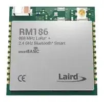
RM186-SM-01
LoRa + Bluetooth® Module, LPWAN EIoT Applications, 863 to 870Mhz, 50KBPS
⚠️ Reference pricing provided. In case of supply shortages, we will connect you with our trusted procurement partners to ensure your project's continuity.
- Manufacturer: EZURIO
- Product type: Bluetooth Modules & Adaptors
- Bluetooth Version:Bluetooth 4.0; Supply Voltage Min:1.8V; Supply Voltage Max:3.6V; Signal Range Max:15km; Data Rate:50Kbps; Bluetooth Class:-; Receive Sensitivity:135dBm; Operating
- SVHC: No SVHC (19-Jan-2021)
- Interfaces: I2C, SPI, UART
- Product Range: RM1xx Series
- Certifications: EU
- Bluetooth Class: -
- Bluetooth Version: Bluetooth 4.0
- Supply Voltage Range: 1.8 V to 3.6 V
- Receiver Sensitivity Rx: 135 dBm
- Operating Temperature Range: -40 °C to 85 °C
| Delivery and price | |
|---|---|
| Units per pack | 100 |
| Price | 17.52 € |
| Current stock | 10+ |
| Lead time | 30 days |
Datasheet

A
**==> picture [470 x 377] intentionally omitted <==**
**----- Start of picture text -----**<br>
Datasheet<br>LoRa/Bluetooth Low Energy (BLE) Module<br>Part Numbers: RM186 and RM7191<br>Version 3.1<br>End of Life<br>**----- End of picture text -----**<br>
|**Version**|**Date**||**Notes**||**Contributor(s)**<br>**Approver**|
|---|---|---|---|---|---|
|1.0|19 May 2016||Initial version||Jonathan Kaye|
|1.1|20 May 2016||Updated SIG section with URL to listing||Jonathan Kaye|
|1.2|11 Aug 2016||Changed_Hardware Integration Guide_to_Datasheet_||Sue White|
|1.3<br>1.4<br>1.5<br>1.6<br>1.7<br>1.8<br>1.9<br>1.10<br>2.0<br>3.0<br>3.1|2 Nov 2016<br>Updated section numbers<br>Sue White<br>01 Feb 2017<br>Updated to include BLE Peripheral Mode<br>Jonathan Kaye<br>17 Oct 2017<br>Added sectionRM1xx VSP Service and Modes.<br>Notes to clarify that JTAG is required when flashing<br>between central and peripheral firmware.<br>Raj Khatri<br>3 Nov 2017<br>UpdatedMechanical Detailsto indicate pin 1.<br>Sue White<br>20 Mar 2018<br>Fix Pin 7 in Pin Definitions Table to Pull Down<br>Raj Khatri<br>29 Oct 2018<br>Updated template; added Australia certification info;<br>replaced BTv4.0 with BTv4.1<br>Maggie Teng<br>Jonathan Kaye<br>14 Feb 2019<br>Updated logos and URLs<br>Sue White<br>28 Mar 2019<br>Added new antenna to FCC regulatory section<br>Maggie Teng<br>Jonathan Kaye<br>20 Sept 2019<br>Added NCC and ASNZS regulatory sections<br>Maggie Teng<br>Jonathan Kaye<br>15 Dec 2020<br>Updated all regulatory information<br>Maggie Teng<br>Ryan Urness<br>Jonathan Kaye<br>21 Feb 2021<br>Transferred all detailed regulatory information to a<br>separate document<br>Sue White<br>Jonathan Kaye<br>End of Life|||||
|https://www.lairdconnect.com/wireless-|||2||**Americas**: +1-800-492-2320|
|modules/lorawan-solutions|||© Copyright 2020 Laird Connectivity, Inc.||**Europe**: +44-1628-858-940|
||||All Rights Reserved||**Hong Kong**: +852 2923 0610|
**Americas** : +1-800-492-2320 **Europe** : +44-1628-858-940 **Hong Kong** : +852 2923 0610
|1|Overview and Key Features ................................................................................................................................................ 4|
|---|---|
|2|Specifications ...................................................................................................................................................................... 4|
|3|Hardware Specifications ...................................................................................................................................................... 8|
||3.1<br>Block Diagram and Pin-out ......................................................................................................................................... 8|
||3.2<br>Pin Definitions ............................................................................................................................................................ 9|
|4<br>5<br>6<br>7|3.3<br>Electrical Specifications ............................................................................................................................................ 11<br>Functional Description ....................................................................................................................................................... 18<br>4.1<br>Power Management (includes brown-out and power on reset) ................................................................................ 18<br>4.2<br>Clocks and Timers.................................................................................................................................................... 18<br>4.3<br>RF ............................................................................................................................................................................ 19<br>4.4<br>UART Interface ........................................................................................................................................................ 19<br>4.5<br>SPI Bus .................................................................................................................................................................... 20<br>4.6<br>I2C Interface ............................................................................................................................................................. 20<br>4.7<br>General Purpose I/O, ADC and PWM/FREQ ........................................................................................................... 21<br>4.8<br>nRESET Pin ............................................................................................................................................................. 21<br>4.9<br>nAutoRUN Pin .......................................................................................................................................................... 21<br>4.10<br>RM1xx VSP Service and Modes .............................................................................................................................. 22<br>4.11<br>Two-Wire SWD Programming/Debug Interface ........................................................................................................ 22<br>4.12<br>RM1xx on-board chip antenna characteristics ......................................................................................................... 23<br>Hardware Integration Suggestions .................................................................................................................................... 23<br>5.1<br>Circuit ....................................................................................................................................................................... 23<br>5.2<br>PCB Layout on Host PCB – General ........................................................................................................................ 25<br>5.3<br>LoRa External Antenna Integration with RM1xx ....................................................................................................... 27<br>Mechanical Details ............................................................................................................................................................ 27<br>Application Note for Surface Mount Modules..................................................................................................................... 29<br>7.1<br>Introduction .............................................................................................................................................................. 29<br>7.2<br>Shipping ................................................................................................................................................................... 29<br>7.3<br>Reflow Parameters ................................................................................................................................................... 30<br>End of Life|
|8|Regulatory ......................................................................................................................................................................... 31|
|9|Ordering Information .......................................................................................................................................................... 32|
|10|Bluetooth SIG Qualification ............................................................................................................................................... 32|
|11|Additional Assistance ........................................................................................................................................................ 33|
https://www.lairdconnect.com/wirelessmodules/lorawan-solutions
**Americas** : +1-800-492-2320 **Europe** : +44-1628-858-940 **Hong Kong** : +852 2923 0610
3 © Copyright 2020 Laird Connectivity, Inc. All Rights Reserved
## **This Datasheet describes both the RM186 (868 MHz band for EU) and RM191 (915 MHz band for US). The differences are outlined in the radio specifications.**
- Every RM1xx Series module is designed to enable OEMs to add a long range LoRa radio link and either Central OR Peripheral mode Bluetooth Low Energy (BLE) to small, portable, power-conscious devices. The RM1xx modules are enabled with Laird’s _smart_ BASIC, an event-driven programming language that enables OEMs to make their product development quicker and simpler, significantly reducing time to market. _smart_ BASIC enables customers to develop a complete embedded application inside the compact RM1xx hardware, connecting to a wide array of external sensors via its I2C, SPI, UART, ADC, or GPIO interfaces. Based on the world-leading Nordic Semiconductor nRF51822 (BLE) and Semtech Sx1272 (LoRa) chipsets, the RM1xx modules provide ultra-low power consumption with outstanding wireless range using the LoRa radio link and local BLE ultra-low power consumption with outstanding wireless range using the LoRa radio link and local BLE low power consumption with outstanding wireless range using the LoRa radio link and local BLE connections via three dBm of transmit power. This document should be read in conjunction with the _smart_ BASIC user manual. **Note:** This information in this document is subject to change. Please contact Laird to obtain the most recent version of this document – https://connectivity.lairdtech.com/resources/support.
- 1.1 Featuresand §@ res) Benefits 1.2 Application Areas ▪ Bluetooth v4.1 – Central OR Peripheral Mode ▪ Public or private networks ▪ On-board BLE chip antenna ▪ Irrigation/Agriculture ▪ U.FL for external LoRa antenna ▪ Parking ▪ _smart_ BASIC programming language ▪ Lighting ▪ Bluetooth SIG Listed ▪ Asset tracking ▪ Compact footprint ▪ Tank monitoring ▪ Long range – LoRa range up to 15 km ▪ Smart Home – smoke alarms, ▪ BLE Programmable TX power +3 dBm to -20 dBm heating, ▪ BLE TX whisper mode (-30 dBm, -55 dBm) ▪ Access control – security ▪ BLE RX sensitivity: -91 dBm ▪ Industrial automation – factory ▪ Ultra-low power consumption ▪ Any long range, battery powered ▪ BLE TX: 12.7 mA peak (at +3 dBm @Vcc=3.3V) (See Note 4 in the sensor application _Power Consumption_ section)
- ▪ BLE RX: 11.9 mA peak (@Vcc=3.3V See Note 4 in the _Power Consumption_ section)
- ▪ Standby Doze: 4.2 uA (typical) ▪ Deep Sleep: 750 nA (See Note 4 in the _Power Consumption_ section)
- ▪ UART, GPIO, ADC, PWM FREQ output, TIMERS, I2C, and SPI interfaces
- ▪ Fast time-to-market
Based on the world-leading Nordic Semiconductor nRF51822 (BLE) and Semtech Sx1272 (LoRa) chipsets, the RM1xx modules provide ultra-low power consumption with outstanding wireless range using the LoRa radio link and local BLE ultra-low power consumption with outstanding wireless range using the LoRa radio link and local BLE low power consumption with outstanding wireless range using the LoRa radio link and local BLE connections via three dBm of transmit power. This document should be read in conjunction with the _smart_ BASIC user manual.
- FCC, ISED, NCC, ASNZS (RM191-SM), EU (RM186-SM)
- No external components required
## _**Table 1: Specifications**_
**Categories Feature Implementation LoRa Wireless** LoRa® LoRaWAN 1.01 (End Device)
https://www.lairdconnect.com/wirelessmodules/lorawan-solutions
4 **Americas** : +1-800-492-2320 © Copyright 2020 Laird Connectivity, Inc. **Europe** : +44-1628-858-940 All Rights Reserved **Hong Kong** : +852 2923 0610
|**Categories**|**Feature**|**Implementation**|||
|---|---|---|---|---|
|**Specification**|Frequency|902-928MHz<br>RM191<br>865-870 MHz<br>RM186|||
||Maximum Transmit Power|15.5 dBm<br>RM191|||
||Setting|13.5 dBm<br>RM186|||
||Minimum Transmit Power<br>Setting|1.5 dBm|||
||Receive Sensitivity|-126 dBm<br>-134 dBm<br>RM191 (BW 500 kHz SF 12)<br>RM186(BW 125kHz SF 12)|||
|Range<br>Upto 15 km in free space<br>Raw Data Rates<br>(over the air)<br>250 bps – 50 kbps<br>RM186<br>980 bps – 21.9kbps<br>RM191<br>**BLE Wireless**<br>**Specification**<br>Bluetooth®(BLE)<br>V4.1 – Central OR Peripheral Mode<br>Frequency<br>2.402 - 2.480 GHz<br>Maximum Transmit Power<br>Setting<br>3 dBm (into -1.5 dBi chip antenna)<br>Minimum Transmit Power<br>Setting<br>-20 dBm (in four dB steps) with_smart_BASIC command<br>-16 dBm<br>-12 dBm<br>-8 dBm<br>-4 dBm<br>0 dBm<br>TX Whisper Mode 1<br>Transmit Power<br>-30 dBm (min.) with_smart_BASIC command<br>TX Whisper Mode 2 Transmit<br>Power<br>-55 dBm (min.) with_smart_BASIC command<br>Receive Sensitivity<br>(0.1% BER)<br>-91 dBm typical<br>Link Budget<br>95 dB(@ 1 Mbps)<br>Range<br>Upto 100 m in free space<br>TX Whisper Modes<br>Range reduction feature with TX Whisper modes with<br>_smart_BASIC command.<br>Range<br>(TX Whisper Mode 2)<br><~30 cm<br>Raw Data Rates<br>1 Mbps(over the air)<br>**Host Interface and**<br>**Peripherals**<br>Total<br>14 x Multifunction I/O lines<br>UART<br>TX, RX, CTS, RTS<br>End of Life|||||
|||DCD, RI, DTR, DSR, CTS, RTS (Note 1)|||
|||Default 115200, n, 8, 1|||
|||From 1,200 to 460800 bps|||
||GPIO|Up to 14|||
|||With configurable I/O direction, O/P drive strength|||
|||(standard 0.5 mA or high 5 mA), pull-up/pull-down|||
||ADC|Four 10-bit channels (including ADC reference)|||
|||10-bit resolution|||
|||1.2 V internal reference|||
|https://www.lairdconnect.com/wireless-|https://www.lairdconnect.com/wireless-|5<br>**Americas**: +1-800-492-2320|||
|modules/lorawan-solutions|© Copyright 2020 Laird Connectivity, Inc.|© Copyright 2020 Laird Connectivity, Inc.<br>**Europe**: +44-1628-858-940|||
||All Rights Reserved<br>**Hong Kong**: +852 2923 0610||||
https://www.lairdconnect.com/wireless5 modules/lorawan-solutions © Copyright 2020 Laird Connectivity, Inc. All Rights Reserved
|**Categories**|**Feature**<br>**Implementation**|
|---|---|
||1/1, 2/3, 1/3 pre-scaling|
||PWM or FREQ output<br>PWM or FREQ output on up to two GPIO output pins:|
||PWM output duty cycle<br>0%-100%|
||PWM output frequency<br>Up to 500 kHz (Note 7)|
||FREQ output frequency<br>0 MHz-4 MHz|
||(50% duty cycle)|
||I2C<br>One I2C interface (up to 400 kbps) (Note 2)|
|SPI<br>One SPI Master interface (up to 4 Mbps) (Note 3)<br>**BLE Services**<br>Services supported<br>GATT client and capabilities<br>**FW Upgrade**<br>_smart_BASIC runtime engine FW<br>upgrade<br>(1) Via UART<br>(2) Via 2-Wire SWD Programming/Debug Interface<br>**Note:**JTAG required for upgrading between Central and<br>Peripheral firmware.<br>**Programmability**<br>_smart_BASIC<br>On-board programming language similar to BASIC.<br>_smart_BASIC application<br>download<br>(1) Via UART.<br>(2) Via Over the Air (If SIO_28 pin is pulled high<br>externally). Only for Peripheral role.<br>**Control Protocols**<br>Any<br>User defined via_smar_tBASIC<br>**Operating Modes**<br>Self-contained Run mode<br>Selected by nAutoRun pin status:<br>nAutoRun = LOW (0V): Then runs $autorun$ (_smart_BASIC<br>application script) if it exists.<br>Interactive / development mode<br>nAutoRun = HIGH (VCC): Then runs via at+run (and “file<br>name” of_smart_BASIC application script).<br>**Supply Voltage**<br>Supply (VCC)<br>2.1V – 3.5V<br>Internal DCDC converter (Note 5)<br>1.8V – 2.1V<br>Internal LDO<br>DCDC switched on if VCC >2.1V atpower-up<br>**BLE Power**<br>**Consumption**<br>Active modes peak current<br>(for Max TX PWR 3 dBm)<br>Connected mode<br>(Vcc=3.3V)<br>12.7 mA peak TX<br>11.9 mA peak RX<br>Active modes peak current<br>(for TX Whisper mode2 PWR<br>-55 dBm)<br>Connected mode<br>(Vcc=3.3V)<br>5 mA peak TX<br>11.9 mA peak RX<br>End of Life||
||Active modes average current<br>Depends on many factors. See_Power Consumption._|
||Ultra-low power modes<br>Standby Doze<br>4.2 uA typical (Note 6)|
||Deep Sleep<br>750 nA (Note 6)|
|**Antenna Options**|BLE (Internal) chip antenna<br>On-board ceramic chip monopole antenna|
||-1.5 dBi|
||LoRa (External)<br>Dipole antenna with U.FL (IPEX) connector up to 2 dBi|
|**Physical**|Dimensions<br>25.4 mm x 25.4 mm x 3.1 mm|
||Weight<br>3 grams|
https://www.lairdconnect.com/wireless6 **Americas** : +1-800-492-2320 modules/lorawan-solutions © Copyright 2020 Laird Connectivity, Inc. **Europe** : +44-1628-858-940 All Rights Reserved **Hong Kong** : +852 2923 0610
|**Categories**<br>**Feature**<br>**Implementation**|
|---|
|**Environmental**<br>Operating<br>-40 ˚C to +85 ˚C (VCC 1.8V – 3.5 V)|
|Storage<br>-40 ˚C to +85 ˚C|
|**Miscellaneous**<br>Lead Free<br>Lead-free and RoHS compliant|
|Warranty<br>1-Year Warranty|
|**Development Tools**<br>Development Kit<br>Development Kit DVK-RM1xx and|
|Free Software Tools|
|**Approvals**<br>Bluetooth®<br>SIG Listed – Declaration ID|
|FCC/ISED/EU/NCC/RCM<br>RM191-SM: FCC/IC/NCC/RCM, RM186-SM: EU<br>**Note 1:**<br>DSR, DTR, RI, and DCD can be implemented in the_smart_BASIC application.<br>**Note 2:**With I2C interface selected, pull-up resistors on I2C SDA and I2C SCL MUST be connected<br>externally as per<br>I2C standard.<br>**Note 3:**SPI interface (master) consists of SPI MOSI, SPI MISO and SPI CLK. SPI CS is created by<br>customer using<br>any spare SIO pin within their_smart_BASIC application script allowing multi-<br>dropping.<br>**Note 4:**RM1xx module comes loaded with_smart_BASIC runtime engine FW, but does not come loaded with any_smart_BASIC<br>application script (as that is dependent on customer end application or use). Laird provides many sample_smart_BASIC<br>application scripts covering the services listed. Additional applications being added every quarter.<br>**Note 5:**Laird suggests using Vcc of 3.3V +/-5% (3.13V-3.46V) for maximum LoRa output power.<br>**_WARNING: above 3.5V, the LoRa transmitter will be disabled to maintain regulatory compliance_**<br>**Note 6:**Deep Sleep current <750nA (typical).<br>Standby Doze current 4.2uA (typical).<br>**Note 7:**PWM output signal has a frequency and duty cycle property. PWM output is generated using 32-bit hardware timers. The<br>timers are clocked by a 1MHz (1uS period) clock source. Trade-off PWM output frequency with resolution. For example:<br>PWM output frequency of 500kHz (2uS) results in resolution of 1:2<br>PWM<br>output frequency of 100kHz (10uS) results in resolution of 1:10<br>PWM output frequency of<br>10kHz (100uS) results in resolution of 1:100<br>PWM output frequency of<br>1kHz(1000uS) results in resolution of 1:1000<br>Refer to the_smart_BASIC user guide for details.<br>End of Life|
https://www.lairdconnect.com/wirelessmodules/lorawan-solutions
**Americas** : +1-800-492-2320 **Europe** : +44-1628-858-940 **Hong Kong** : +852 2923 0610
7 © Copyright 2020 Laird Connectivity, Inc. All Rights Reserved
**==> picture [446 x 550] intentionally omitted <==**
**----- Start of picture text -----**<br>
—<br>FLASH smartBASIC smartBASIC<br>Lees run-time engine<br>(provides safe access to LoRa®*/BLE<br><I> Lora BLE Radio stacks, drivers and non-vol stores)<br>Radio ro PSUand Gem)<br>1_ Management _,<br>2.768409<br>Figure 1: Functional HW and SW block diagram for RM1xx series smartBASIC modules<br>5 GND GND a<br>3 SIO_21 NC —55<br>4 SIO_22 nRESET 21<br>5 SIO_23 GND 59<br>6 SIO_24 SIO_6/AIN 4g<br>7 SIO_25 SIO_5/AIN 18<br>g SIO_28 SIO_4/AIN 47<br>g GND SIO_3/AIN 46<br>49 SIO_29 SIO_17 45<br>44 SIO_30 SIO_00 44<br>12 GND GND 13<br>VCC_BLE VCC_LORA<br>Figure 2: RM186/RM191 module pin-out (top view)<br>https://www.lairdconnect.com/wireless- 8<br>modules/lorawan-solutions © Copyright 2020 Laird Connectivity, Inc.<br> All Rights Reserved<br>End of Life<br>**----- End of picture text -----**<br>
https://www.lairdconnect.com/wirelessmodules/lorawan-solutions
**Americas** : +1-800-492-2320 **Europe** : +44-1628-858-940 **Hong Kong** : +852 2923 0610
_**Table 2: Pin definitions**_
|**Pin #**|**Pin**|**Default**|**Alt.**|**Default**|**Pull-**|**Notes**|**Comment**|
|---|---|---|---|---|---|---|---|
||**Name**|**Function**|**Funct.**|**Direction**|**up/**|||
|||||**Note14**|**Pull-**|||
||||||**down**|||
||||||**Note14**|||
|1|GND|-|-|-|-|-|-|
|2<br>3<br>4<br>5<br>6<br>7<br>8<br>9<br>10<br>11<br>12<br>13<br>14<br>15<br>16<br>17|SIO_21<br>DIO<br>UART TX<br>OUT<br>Set<br>high in<br>FW<br>1,2,4,6,7<br>UARTCLOSE() selects DIO<br>functionality and<br>UARTOPEN() selects UART<br>comms behaviour<br>SIO_22<br>DIO<br>UART RX<br>IN<br>PULL-<br>UP<br>1,2,4,6,7<br>SIO_23<br>DIO<br>UART RTS<br>OUT<br>Set low<br>in FW<br>1,2,4,6,7<br>SIO_24<br>DIO<br>UART CTS<br>IN<br>PULL-<br>DOWN<br>1,2,4,6,7<br>SIO_25<br>nAutoRUN/DIO<br>DIO<br>IN<br>NONE<br>IN only<br>Laird Devkit, UART_DSR via<br>J10, J12<br>SIO_28<br>vSP/DIO<br>DIO<br>IN<br>PULL-<br>DOWN<br>1,2,6,12,13<br>Laird DevKit: J6 (vSP/OTA)<br>GND<br>-<br>-<br>-<br>-<br>-<br>SIO_29<br>DIO<br>I2C SCL<br>IN<br>PULL-<br>UP<br>1,2,6,11<br>I2COPEN() in_smart_BASIC<br>selects I2C function<br>SIO_30<br>DIO<br>I2C SDA<br>IN<br>PULL-<br>UP<br>1,2,6,11<br>GND<br>VCC_BLE<br>-<br>-<br>-<br>-<br>-<br>Vcc for BLE Radio<br>VCC_LORA<br>-<br>-<br>-<br>-<br>-<br>Vcc for Lora Radio<br>GND<br>-<br>-<br>-<br>-<br>-<br>SIO_00<br>DIO<br>SPI CLK<br>IN<br>PULL-<br>UP<br>1,2,6,11<br>SPIOPEN() in_smart_BASIC<br>selects SPI function, MOSI<br>and CLK will be outputs when<br>in SPI master mode. See note<br>11<br>SIO_17<br>DIO<br>SPI MISO<br>IN<br>PULL-<br>UP<br>1,2,6,11<br>SIO_03/AIN<br>DIO/AIN<br>SPI MOSI<br>IN<br>PULL-<br>UP<br>1,2,3,4,5,6,11<br>End of Life|||||||
|18|SIO_04/AIN|DIO|AIN|IN|PULL-<br>UP|1,2,3,4,5,6,11|Laird Devkit: SPI Slave Select|
|19|SIO_05/AIN|DIO|AIN|IN|PULL-<br>UP|1,2,3,4,5,6,11|Laird Devkit: Button2 or Ana<br>TempSensor via J7|
|20|SIO_06/AIN|DIO|AIN|IN|PULL-<br>UP|1,2,3,4,5,6,11|Laird Devkit: LED5 or Arduino<br>A0 Via J8|
|21|GND|||||||
|22|nRESET|||IN||9,10|System Reset(Active low)|
|23|NC|||||9|DO NOT CONNECT|
|24|GND|||||||
https://www.lairdconnect.com/wireless9 modules/lorawan-solutions © Copyright 2020 Laird Connectivity, Inc. All Rights Reserved
**Americas** : +1-800-492-2320 **Europe** : +44-1628-858-940 **Hong Kong** : +852 2923 0610
## **Note 1:** Secondary function is selectable in _smart_ BASIC application.
**Note 2:** DIO = Digital Input or Output. I/O voltage level tracks VCC.
- **Note 3:** AIN = Analog Input
**Note 4:** DIO or AIN functionality is selected using the GpioSetFunc() function in _smart_ BASIC. **Note 5:** AIN configuration selected using GpioSetFunc() function. **Note 6:** I2C, UART, SPI controlled by xxxOPEN() functions in _smart_ BASIC. **Note 7:** SIO_21 to SIO_24 are DIO by default when $autorun$ app runs on power up. **Note 8:** N/A **Note 9:** Hidden 2-Wire SWD Programming/Debug Interface (JTAG), pin22 (SWDIO) and pin23 (SWDCLK). Used for upgrading _smart_ BASIC runtime engine FW with J-link programmer. Using this hidden 2-Wire SWD Programming/Debug Interface on customers host PCB requires header connector Samtec FTSH-10501-L-DV, refer to section _**2-Wire SWD Programming/Debug Interface**_ for details. **JTAG required for upgrading between Central and Peripheral firmware. Note 10:** Pull the nRESET pin (pin 22) low for minimum 100 mS to reset the module. **Note11:** SPI CS is created by customer using any spare SIO pin within their _smart_ BASIC application script allowing multi-dropping. **Note12:** SIO_28 pin must be pulled high externally to enable OTA (over the Air) smartBASIC application download. Refer to the latest FW release documentation for details. **Note13:** User must ensure that SIO_28 and AutoRUN (SIO_25) are NOT BOTH HIGH (externally), otherwise in that state the UART is bridged to Virtual Serial Port service and so the RM1xx module will not respond to AT commands and therefore cannot load smartBASIC application scripts (applies to all versions of the smart BASIC runtime engine firmware.) **Note14:** _smart_ BASIC runtime engine has DIO (Default Function) INPUT pins, have by default PULL-UP enabled. This was done to avoid floating inputs (which can also cause current consumption in low power modes (e.g. Standby Doze) to drift with time. In any case customer can disable the PUL-UP through their _smart_ BASIC application. All the SIO pins (with a default function of DIO are inputs – apart from SIO_21 and SIO_23, which are outputs):
- **SIO_21** (alternative function UART_TX) is an output, set high (in FW).
- **SIO_23** (alternative function UART_RTS) is an output, set low (in FW).
- **SIO_22** (alternative function UART_RX) is an input, set with internal pull-up (in FW).
- **SIO_24** (alternative function UART_CTS) is an input, set with internal pull-down (in FW).
The RM1xx module is delivered with the integrated _smart_ BASIC runtime engine FW loaded (but no onboard _smart_ BASIC application script). Because of this, it starts up in AT command mode by default.
https://www.lairdconnect.com/wirelessmodules/lorawan-solutions
**Americas** : +1-800-492-2320 **Europe** : +44-1628-858-940 **Hong Kong** : +852 2923 0610
10 © Copyright 2020 Laird Connectivity, Inc. All Rights Reserved
At reset, all SIO lines are configured as the defaults shown above.
SIO lines can be configured through the _smart_ BASIC application script to be either inputs or outputs with pull-ups or pulldowns. When an alternative SIO function is selected (such as I2C or SPI), the firmware does not allow the setup of internal pull-up/pull-down. Therefore, when I2C interface is selected, pull-up resistors on I2C SDA and I2C SCL **MUST** be connected externally as per I2C standard.
UART_RX, UART_TX, UART_CTS are Vcc logic levels (if VCC is 3.3 V, i.e. SIO pin I/O levels track VCC). For example, when RX and TX are idle, they sit at 3.3 V (if VCC is 3.3 V). Conversely, handshaking pins CTS and RTS at 0 V are treated as assertions.
|Pin 6 (nAutoRUN) is an input, with active low logic. In the development kit (DVK-RM1xx-SM) it is connected so that the state is|
|---|
|driven by the host’s DTR output line. The nAutoRUN pin must be externally held high or low to select between the following|
|two operating modes:<br>▪<br>Self-contained Run mode (nAutoRUN pin held at 0 V).<br>▪<br>Interactive/development mode (nAutoRUN pin held at VCC).<br>_smart_BASIC runtime engine firmware checks for the status of nAutoRUN during power-up or reset. If it is low and if there is a<br>_smart_BASIC application script named**$autorun$**, then the_smart_BASIC runtime engine FW executes the application script<br>automatically; hence the name S_elf-contained Run Mode_.<br>Absolute maximum ratings for supply voltage and voltages on digital and analogue pins of the module are listed below;<br>exceeding these values causes permanent damage (Table 3).<br>**_Table 3: Maximum Current Ratings_**<br>**Parameter**<br>**Minimum**<br>**Maximum**<br>**Unit**<br>Voltage at VCC_BLE and VCC_LORA pin<br>-0.3<br>+3.6 (Note 1)<br>V<br>Voltage at GND pin<br>0<br>V<br>Voltage at SIO pin<br>-0.3<br>VCC+0.3<br>V<br>Storage temperature<br>-40<br>+85<br>ºC<br>**Note 1**:<br>Absolute Max Rating for VCC pin (max) is 3.6V, however we recommend 3.3V +/-5% as the spec for maximum<br>Vcc._The LoRa transmitter shuts down if the voltage exceeds 3.5V_.<br>**_Table 4: Power Supply Operating Parameters_**<br>**Parameter**<br>**Minimum**<br>**Typical**<br>**Maximum**<br>**Unit**<br>VCC**1**<br>1.8<br>3.3<br>3.5<br>V<br>VCC Maximum ripple or noise**2**<br>10<br>mV<br>End of Life<br>3.53<br>Electrical Specifications<br>3.5.1<br>Absolute Maximum Ratings<br>3.5.2 Recommended Operating Parameters|
|Operating Temperature Range<br>-40<br>-<br>+85<br>ºC|
||
|**Note 1:**<br>Internal DCDC is used if VCC >2.1 V on power-up; otherwise internal LDO is used_._|
|_If supply voltage is greater than 3.5V, the LoRa transmitter will be disabled._|
**Note 2:** The maximum VCC ripple or noise (at any frequency) that does not disturb the radio.
## _**Table 5: Signal Levels for Interface, SIO**_
|**_Table 5: Signal Levels for Interface, SIO_**|||||||
|---|---|---|---|---|---|---|
|**Parameter**|**Minimum**||**Typical**|**Maximum**||**Unit**|
|https://www.lairdconnect.com/wireless-||11|11||**Americas**: +1-800-492-2320||
|modules/lorawan-solutions|© Copyright 2020 Laird Connectivity, Inc.|© Copyright 2020 Laird Connectivity, Inc.|||**Europe**: +44-1628-858-940||
||All Rights Reserved||||**Hong Kong**: +852 2923 0610||
https://www.lairdconnect.com/wirelessmodules/lorawan-solutions
|**Parameter**|**Minimum**||**Typical**|**Maximum**||**Unit**|
|---|---|---|---|---|---|---|
|VIH Input high voltage|0.7VCC|||VCC||V|
|VIL Input low voltage|VSS|||0.3||V|
|VOH Output high voltage|||||||
|(std. drive, 0.5mA)|VCC-0.3|||VCC||V|
|(high-drive, 5mA) (Note 1)|VCC-0.3|||VCC||V|
|VOL Output low voltage|||||||
|(std. drive, 0.5mA)|VSS|||0.3||V|
|(high-drive, 5mA) (Note 1)<br>VSS<br>0.3<br>Pull up resistance<br>11<br>13<br>16<br>Pull down resistance<br>11<br>13<br>16<br>**Note 1: **Maximum number of pins with 5mA high drive is three.<br>**_Table 6: SIO pin alternative function AIN (ADC) specification_**<br>**Parameter**<br>**Minimum**<br>**Typical**<br>**Maximum**<br>ADC Internal reference voltage<br>-1.5%<br>1.2 V<br>+1.5%<br>ADC pin input<br>internal selectable scaling<br>1/1, 1/3, 2/3<br>ADC input pin (AIN) voltage maximum<br>without damaging ADC w.r.t<br>VCC Prescaling<br>3.3 V 1/1<br>3.3 V 2/3<br>3.3 V 1/3<br>1.8 V 1/1<br>1.8 V 2/3<br>1.8 V 1/3<br>2.4<br>3.6<br>3.6<br>2.1<br>2.1<br>2.1<br>ADC input pin (AIN) voltage maximum<br>without saturating ADC (with 1.2V internal<br>reference)**1**<br>1/1 prescaling<br>2/3 prescaling<br>1/3 prescaling<br>1.2<br>1.8<br>3.6<br>End of Life||||||V<br>kΩ<br>kΩ<br>**Unit**<br>%<br>Scaling<br>V<br>V<br>V<br>V<br>V<br>V<br>V<br>V<br>V|
|Time required to convert single sample in|||||||
|10bit mode|||68|||uS|
|9bit mode**2**|||36|||uS|
|8 bit mode**2**|||20|||uS|
|ADC input impedance (during operation)3|||||||
## _**Table 6: SIO pin alternative function AIN (ADC) specification**_
**Note 1:** Stay within internal 1.2 V reference voltage with given prescaling on AIN pin and do not violate ADC maximum input voltage (for damage) for a given VCC, e.g. If VCC is 1.8 V can only expose AIN pin to 2.1 V (VCC+0.3).
**Note 2:** Currently, the _smart_ BASIC runtime engine firmware only allows 10-bit mode.
https://www.lairdconnect.com/wirelessmodules/lorawan-solutions
**Americas** : +1-800-492-2320 **Europe** : +44-1628-858-940 **Hong Kong** : +852 2923 0610
12
© Copyright 2020 Laird Connectivity, Inc. All Rights Reserved
**Note 3:** ADC input impedance is estimated mean impedance of the ADC (AIN) pins. The tolerance is +/-20%. The ADC is highly sensitive to the impedance of the source. The ADC (AIN) input impedance is 200k-600k depending on your ADC gain (pre-scaling) setting. Normally, when not sampling, the ADC (AIN) impedance will have very high value and can consider it to be an open circuit. The moment ADC is sampling, ADC (AIN) impedance is 200k600k.
## 3.5.5 NAUtORUN Pin and Operating Modes
Operating modes (refer to the _smart_ BASIC manual for details):
- Self-contained mode
|▪<br>Interactive/Development mode<br>**_Table 7: nAutoRUN pin_**<br>**Signal Name**<br>**Pin #**<br>**I/O**<br>**Comments**<br>nAutoRUN (SIO_25)<br>6<br>I<br>Input with active low logic.<br>Operating mode selected by nAutoRun pin status:<br>If Low (0V), runs $autorun$ if it exists;<br>If High (VCC), runs via at+run (and “file name” of application).<br>Pin 40 (nAutoRUN) is an input, with active low logic. In the development board (DVK-RM1xx) it is connected so that the state<br>is driven by the host’s DTR output line. nAutoRUN pin needs to be externally held high or low to select between the two<br>RM1xx operating modes:<br>▪<br>Self-contained Run mode (nAutoRUN pin held at 0V).<br>▪<br>Interactive/Development mode (nAutoRUN pin held at VCC)<br>_smart_BASIC runtime engine firmware checks for the status of nAutoRUN during power-up or reset. If it is low and if there is a<br>_smart_BASIC application named $autorun$ then the_smart_BASIC runtime engine executes the application automatically; hence<br>the name_self-contained run mode_.<br>To maximize output power, the best choice for module Vcc is 3.3V +/- 5% (which results in a Vcc range of 3.14V to 3.47V).<br>The data inTable 8was taken at 25ºC with UART on and all other peripherals turned off. It shows how the output power and<br>transmitter current consumption falls off as a function of Vcc.<br>**_Table 8: Power consumption and output power vs Vcc_**<br>**RM186**<br>**RM191**<br>**Vcc**<br>**[V]**<br>**Tx Current**<br>**[mA]**<br>**Rx Current**<br>**[mA]**<br>**Pout**<br>**[dBm]**<br>**Tx Current**<br>**[mA]**<br>**Rx Current**<br>**[mA]**<br>**Pout**<br>**[dBm]**<br>3.5<br>31.4<br>12.7<br>13.8<br>45.7<br>15.3<br>15.2<br>3.3<br>30.9<br>12.6<br>13.5<br>43.3<br>15.0<br>14.9<br>End of Life<br>3.5.4 LoRa Output Power and Current Consumption vs Vcc|
|---|
|3.0<br>29.5<br>12.3<br>13.0<br>39.8<br>15.1<br>14.3|
|2.7<br>27.9<br>12.2<br>12.2<br>36.3<br>14.8<br>13.4|
|1.8<br>19.4<br>11.8<br>6.5<br>24.5<br>14.4<br>8.5|
## 3.3.4.1.
The plots below (Figure 3 and Figure 4) depict a typical Transmit/Receive cycle when sending a LoRa packet to the gateway. The plots were made using a shunt current monitor and the voltage levels have been translated to currents. The current plots show a transmitted packet, the first receive window (one second later), followed by the second receive window (one second following the first receive window). The currents represented are the total module current (the sum of VCC_BLE and VCC_LORA pins).
https://www.lairdconnect.com/wirelessmodules/lorawan-solutions
**Americas** : +1-800-492-2320 **Europe** : +44-1628-858-940 **Hong Kong** : +852 2923 0610
13
© Copyright 2020 Laird Connectivity, Inc. All Rights Reserved
|**_Figure 3: Typical RM186 LoRa transmit/receive cycle (full Tx power, Vcc=3.3V, @25°C _**<br>**_Figure 4: Typical LoRa transmit/receive cycle (full Tx power, Vcc=3.3V, @25˚C)_**<br>Table 9tabulates typical LoRa receive sensitivity as a function of the LoRa data rate. The data rate is determined by the<br>combination of bandwidth and spreading factor of the incoming LoRa signal. The data rates in the table are the LoRaWAN<br>data rates used by the gateway when transmitting to the end device.<br>**_Table 9: Receive sensitivity vs LoRa data rate_**<br>End of Life<br>Toturn<br>on<br>cursors,<br>press<br>the [Cursors] key on the front panel<br>OS0-X20244, MY59510658: Wed May 11 11:29:35 2016<br>1<br>2009/<br>1.020s<br>900.02/<br>ig'd<br>$ 1<br>5638<br>Agilent<br>Tx<br>Acquisition<br>43.3mA<br>poe<br>n<br>Channels<br>If<br>[<br>1<br>Rx Win #1<br>Rx Win #2<br>15mA<br>15mA<br>Je<br>Cursors<br>Men<br>To turn<br>on cursors,<br>press<br>the<br>[Cursors]<br>key on the front pane!<br>3.5.5 LoRa Receive Sensitivity vs Data Rate|**_Figure 3: Typical RM186 LoRa transmit/receive cycle (full Tx power, Vcc=3.3V, @25°C _**<br>**_Figure 4: Typical LoRa transmit/receive cycle (full Tx power, Vcc=3.3V, @25˚C)_**<br>Table 9tabulates typical LoRa receive sensitivity as a function of the LoRa data rate. The data rate is determined by the<br>combination of bandwidth and spreading factor of the incoming LoRa signal. The data rates in the table are the LoRaWAN<br>data rates used by the gateway when transmitting to the end device.<br>**_Table 9: Receive sensitivity vs LoRa data rate_**<br>End of Life<br>Toturn<br>on<br>cursors,<br>press<br>the [Cursors] key on the front panel<br>OS0-X20244, MY59510658: Wed May 11 11:29:35 2016<br>1<br>2009/<br>1.020s<br>900.02/<br>ig'd<br>$ 1<br>5638<br>Agilent<br>Tx<br>Acquisition<br>43.3mA<br>poe<br>n<br>Channels<br>If<br>[<br>1<br>Rx Win #1<br>Rx Win #2<br>15mA<br>15mA<br>Je<br>Cursors<br>Men<br>To turn<br>on cursors,<br>press<br>the<br>[Cursors]<br>key on the front pane!<br>3.5.5 LoRa Receive Sensitivity vs Data Rate|
|---|---|
|**DR**<br>**Bit Rate**<br>**[Bits/s]**<br>**BW**<br>**[kHz]**<br>**SF**<br>**Rx Sensitivity**<br>**[dBm]**||
|8<br>980<br>500<br>12<br>-126||
|9<br>1760<br>500<br>11<br>-125||
|10<br>3900<br>500<br>10<br>-122||
|RM191||
|11<br>7000<br>500<br>9<br>-119||
|12<br>12500<br>500<br>8<br>-116||
|13<br>21900<br>500<br>7<br>-113||
https://www.lairdconnect.com/wirelessmodules/lorawan-solutions
**Americas** : +1-800-492-2320 **Europe** : +44-1628-858-940 **Hong Kong** : +852 2923 0610
14 © Copyright 2020 Laird Connectivity, Inc. All Rights Reserved
||**DR**|**Bit Rate**<br>**[Bits/s]**|**BW**<br>**[kHz]**|**SF**|**Rx Sensitivity**<br>**[dBm]**|
|---|---|---|---|---|---|
||0|250|125|12|-134|
||1|440|125|11|-132|
||2|980|125|10|-130|
|RM186|3|1760|125|9|-127|
||4|3125|125|8|-124|
||5<br>End of Life|5470<br>End of Life|125<br>End of Life|7<br>End of Life|-121<br>End of Life|
||6<br>End of Life|11000<br>End of Life|250<br>End of Life|7<br>End of Life|-119<br>End of Life|
|6<br>11000<br>250<br>7<br>-119<br>Note the following:<br>▪<br>DR = LoRaWAN data rate<br>▪<br>Bit rate is the effective over the air bit rate<br>▪<br>BW is the bandwidth of the incoming LoRa transmission<br>▪<br>SF is the Spreading Factor of the incoming LoRa transmission<br>Data taken at VCC 3.3V (see Note 1 followingTable 10) and 25ºC.<br>**_Table 10: Power consumption_**<br>**Parameter**<br>**Min**<br>**Typical**<br>**Max**<br>**Active Mode ‘peak’ current – (Note 1)**<br>**(Connection)**<br>TX only run peak current @TXpwr= + 3 dBm<br>TX only run peak current @T pwr= 0 dBm<br>TX only run peak current @TXpwr= -4 dBm<br>TX only run peak current @TXpwr= -8 dBm<br>TX only run peak current @TXpwr= -12 dBm<br>TX only run peak current @TXpwr= -16 dBm<br>T X only run peak current @TXpwr= -20 dBm<br>**TX Whisper Mode 1**<br>TX only run peak current @TXpwr= -30 dBm<br>**TX Whisper Mode 2**<br>TX only run peak current @TXpwr= -55 dBm<br>12.7<br>8.4<br>7.1<br>6.9<br>6.4<br>6.1<br>5.5<br>5.4<br>5.0<br>End of Life<br>3.5.6 BLE Power Consumption|6<br>11000<br>250<br>7<br>-119<br>Note the following:<br>▪<br>DR = LoRaWAN data rate<br>▪<br>Bit rate is the effective over the air bit rate<br>▪<br>BW is the bandwidth of the incoming LoRa transmission<br>▪<br>SF is the Spreading Factor of the incoming LoRa transmission<br>Data taken at VCC 3.3V (see Note 1 followingTable 10) and 25ºC.<br>**_Table 10: Power consumption_**<br>**Parameter**<br>**Min**<br>**Typical**<br>**Max**<br>**Active Mode ‘peak’ current – (Note 1)**<br>**(Connection)**<br>TX only run peak current @TXpwr= + 3 dBm<br>TX only run peak current @T pwr= 0 dBm<br>TX only run peak current @TXpwr= -4 dBm<br>TX only run peak current @TXpwr= -8 dBm<br>TX only run peak current @TXpwr= -12 dBm<br>TX only run peak current @TXpwr= -16 dBm<br>T X only run peak current @TXpwr= -20 dBm<br>**TX Whisper Mode 1**<br>TX only run peak current @TXpwr= -30 dBm<br>**TX Whisper Mode 2**<br>TX only run peak current @TXpwr= -55 dBm<br>12.7<br>8.4<br>7.1<br>6.9<br>6.4<br>6.1<br>5.5<br>5.4<br>5.0<br>End of Life<br>3.5.6 BLE Power Consumption|6<br>11000<br>250<br>7<br>-119<br>Note the following:<br>▪<br>DR = LoRaWAN data rate<br>▪<br>Bit rate is the effective over the air bit rate<br>▪<br>BW is the bandwidth of the incoming LoRa transmission<br>▪<br>SF is the Spreading Factor of the incoming LoRa transmission<br>Data taken at VCC 3.3V (see Note 1 followingTable 10) and 25ºC.<br>**_Table 10: Power consumption_**<br>**Parameter**<br>**Min**<br>**Typical**<br>**Max**<br>**Active Mode ‘peak’ current – (Note 1)**<br>**(Connection)**<br>TX only run peak current @TXpwr= + 3 dBm<br>TX only run peak current @T pwr= 0 dBm<br>TX only run peak current @TXpwr= -4 dBm<br>TX only run peak current @TXpwr= -8 dBm<br>TX only run peak current @TXpwr= -12 dBm<br>TX only run peak current @TXpwr= -16 dBm<br>T X only run peak current @TXpwr= -20 dBm<br>**TX Whisper Mode 1**<br>TX only run peak current @TXpwr= -30 dBm<br>**TX Whisper Mode 2**<br>TX only run peak current @TXpwr= -55 dBm<br>12.7<br>8.4<br>7.1<br>6.9<br>6.4<br>6.1<br>5.5<br>5.4<br>5.0<br>End of Life<br>3.5.6 BLE Power Consumption|6<br>11000<br>250<br>7<br>-119<br>Note the following:<br>▪<br>DR = LoRaWAN data rate<br>▪<br>Bit rate is the effective over the air bit rate<br>▪<br>BW is the bandwidth of the incoming LoRa transmission<br>▪<br>SF is the Spreading Factor of the incoming LoRa transmission<br>Data taken at VCC 3.3V (see Note 1 followingTable 10) and 25ºC.<br>**_Table 10: Power consumption_**<br>**Parameter**<br>**Min**<br>**Typical**<br>**Max**<br>**Active Mode ‘peak’ current – (Note 1)**<br>**(Connection)**<br>TX only run peak current @TXpwr= + 3 dBm<br>TX only run peak current @T pwr= 0 dBm<br>TX only run peak current @TXpwr= -4 dBm<br>TX only run peak current @TXpwr= -8 dBm<br>TX only run peak current @TXpwr= -12 dBm<br>TX only run peak current @TXpwr= -16 dBm<br>T X only run peak current @TXpwr= -20 dBm<br>**TX Whisper Mode 1**<br>TX only run peak current @TXpwr= -30 dBm<br>**TX Whisper Mode 2**<br>TX only run peak current @TXpwr= -55 dBm<br>12.7<br>8.4<br>7.1<br>6.9<br>6.4<br>6.1<br>5.5<br>5.4<br>5.0<br>End of Life<br>3.5.6 BLE Power Consumption|6<br>11000<br>250<br>7<br>-119<br>Note the following:<br>▪<br>DR = LoRaWAN data rate<br>▪<br>Bit rate is the effective over the air bit rate<br>▪<br>BW is the bandwidth of the incoming LoRa transmission<br>▪<br>SF is the Spreading Factor of the incoming LoRa transmission<br>Data taken at VCC 3.3V (see Note 1 followingTable 10) and 25ºC.<br>**_Table 10: Power consumption_**<br>**Parameter**<br>**Min**<br>**Typical**<br>**Max**<br>**Active Mode ‘peak’ current – (Note 1)**<br>**(Connection)**<br>TX only run peak current @TXpwr= + 3 dBm<br>TX only run peak current @T pwr= 0 dBm<br>TX only run peak current @TXpwr= -4 dBm<br>TX only run peak current @TXpwr= -8 dBm<br>TX only run peak current @TXpwr= -12 dBm<br>TX only run peak current @TXpwr= -16 dBm<br>T X only run peak current @TXpwr= -20 dBm<br>**TX Whisper Mode 1**<br>TX only run peak current @TXpwr= -30 dBm<br>**TX Whisper Mode 2**<br>TX only run peak current @TXpwr= -55 dBm<br>12.7<br>8.4<br>7.1<br>6.9<br>6.4<br>6.1<br>5.5<br>5.4<br>5.0<br>End of Life<br>3.5.6 BLE Power Consumption|**Unit**<br>mA<br>mA<br>mA<br>mA<br>mA<br>mA<br>mA<br>mA<br>mA|
|---|---|---|---|---|---|
|**Active Mode**||||||
|RX only ‘peak’ current||11.9|||mA|
|**Ultra Low Power Mode1 (Note 2)**||||||
|Standby Doze||4.2|||uA|
|**Ultra Low Power Mode2 (Note 3)**||||||
|Deep Sleep (no RAM retention)||750|||nA|
Note the following:
## 3.5.6 BLE Power Consumption
Data taken at VCC 3.3V (see Note 1 following Table 10) and 25 º C.
## _**Table 10: Power consumption**_
https://www.lairdconnect.com/wirelessmodules/lorawan-solutions
**Americas** : +1-800-492-2320 **Europe** : +44-1628-858-940 **Hong Kong** : +852 2923 0610
15 © Copyright 2020 Laird Connectivity, Inc. All Rights Reserved
**Parameter Min Typical Max Unit Active Mode Average current (Note 4) Connection Average Current draw Max** with connection interval (min) 7.5 mS with connection interval 67.5 mS ~400 uA **Min** with connection interval (max) 4000 mS ~2.6-4.1 uA **Note 1:** If VCC is below 2.1V (operating range of DCDC), the peak current consumption will increase because the DCDC converter is switched off and the internal LDO is enabled. **Note 2:** Standby Doze is entered automatically (when _waitevent_ statement is encountered within a _smart_ BASIC application script). See individual peripherals current consumption in tables in section _**Peripheral block current consumption 4.3**_ . **Note 3:** In Deep Sleep, everything is disabled and the only wake-up sources are reset and changes on pins on which sense is enabled. A reset is required to exit Deep Sleep. **Note 4:** Data taken with TX power 3 dBm and all peripherals off (UART OFF after radio event). Average current consumption depends on a number of factors (including TX power, VCC and accuracy of 16 MHz and 32.768 kHz crystals). With these factors fixed, the largest variable is the connection interval. **Connection Interval Range:** 7.5 ms to 4000 ms in multiples of 1.25 ms. **For a connection event:** – The minimum average current consumption is when the connection interval is large 4000 mS – The maximum average current consumption is with the shortest connection interval of 7.5 ms; no slave latency. Other factors that are also related to average current consumption include whether transmitting 6 packets per connection interval & each packet contains 20 bytes (which is the maximum for each packet) and an inaccurate 32 kHz master clock accuracy would increase the average current consumption. 3.3.6.1 BLE Measured Measured Peak Current Waveforms during Connection Figure 5 illustrates BLE current waveforms observed as the RM1xx module performs a transmit/receive cycle with Vcc = 3.3V. illustrates BLE current waveforms observed as the RM1xx module performs a transmit/receive cycle with Vcc = 3.3V. The plot was made using a shunt current sensor and the voltage waveform has been manually converted to current. The current represented is the total module current which is the sum of the BLE_VCC and BLE_LORA pins.
**Note 3:** In Deep Sleep, everything is disabled and the only wake-up sources are reset and changes on pins on which sense is enabled. A reset is required to exit Deep Sleep. **Note 4:** Data taken with TX power 3 dBm and all peripherals off (UART OFF after radio event). Average current consumption depends on a number of factors (including TX power, VCC and accuracy of 16 MHz and 32.768 kHz crystals). With these factors fixed, the largest variable is the connection interval.
3.3.6.1 BLE Measured Measured Peak Current Waveforms during Connection Figure 5 illustrates BLE current waveforms observed as the RM1xx module performs a transmit/receive cycle with Vcc = 3.3V. illustrates BLE current waveforms observed as the RM1xx module performs a transmit/receive cycle with Vcc = 3.3V. The plot was made using a shunt current sensor and the voltage waveform has been manually converted to current. The current represented is the total module current which is the sum of the BLE_VCC and BLE_LORA pins.
https://www.lairdconnect.com/wirelessmodules/lorawan-solutions
**Americas** : +1-800-492-2320 **Europe** : +44-1628-858-940 **Hong Kong** : +852 2923 0610
16 © Copyright 2020 Laird Connectivity, Inc. All Rights Reserved
**BLE Transmit/Receive currents at Vcc=3.3V @25˚C**
|**_Figure 5: Typical peak current consumption profile with doze mode in effect before/after the Rx/Tx_**<br>**_Table 11: BLE Peak Transmit/Receive currents vs Vcc @25˚C_**<br>**Vcc**<br>**[V]**<br>**BLE Tx Current**<br>**[mA]**<br>**BLE Rx Current**<br>**[mA]**<br>3.5<br>12.0<br>11.4<br>3.3<br>12.7<br>11.9<br>3.0<br>13.3<br>12.3<br>2.7<br>14.4<br>13.0<br>1.8<br>16.6<br>15.02<br>**Note:**<br>This is the total module current (sum of pins VCC_BLE and VCC_LORA)<br>The values below are calculated for a typical operating voltage of 3 V.<br>**_Table 12: UART Power Consumption_**<br>**Parameter**<br>**Min**<br>**Typ**<br>**Max**<br>**Unit**<br>UART Run current @ Max Baud Rate<br>230<br>uA<br>UART Run current @ 115200 bps<br>220<br>uA<br>UART Run current @ 1200 bps<br>210<br>uA<br>End of Life<br>>en<br>enieeenanneeammamnne<br>a<br>awe<br>ji<br>Recall<br>Default/Erase<br>Pre<br>to<br>3.3.6.2 Peripheral Block Current Consumption|**_Figure 5: Typical peak current consumption profile with doze mode in effect before/after the Rx/Tx_**<br>**_Table 11: BLE Peak Transmit/Receive currents vs Vcc @25˚C_**<br>**Vcc**<br>**[V]**<br>**BLE Tx Current**<br>**[mA]**<br>**BLE Rx Current**<br>**[mA]**<br>3.5<br>12.0<br>11.4<br>3.3<br>12.7<br>11.9<br>3.0<br>13.3<br>12.3<br>2.7<br>14.4<br>13.0<br>1.8<br>16.6<br>15.02<br>**Note:**<br>This is the total module current (sum of pins VCC_BLE and VCC_LORA)<br>The values below are calculated for a typical operating voltage of 3 V.<br>**_Table 12: UART Power Consumption_**<br>**Parameter**<br>**Min**<br>**Typ**<br>**Max**<br>**Unit**<br>UART Run current @ Max Baud Rate<br>230<br>uA<br>UART Run current @ 115200 bps<br>220<br>uA<br>UART Run current @ 1200 bps<br>210<br>uA<br>End of Life<br>>en<br>enieeenanneeammamnne<br>a<br>awe<br>ji<br>Recall<br>Default/Erase<br>Pre<br>to<br>3.3.6.2 Peripheral Block Current Consumption|
|---|---|
|UART Baud rate<br>1200<br>460800|bps|
|**_Table 13: SPI Power Consumption_**||
|**Parameter**<br>**Min**<br>**Typ**<br>**Max**|**Unit**|
|SPI Master Run current @ 125 kbps<br>180|uA|
|SPI Master Run current @ 4 Mbps<br>200|uA|
|SPI bit rate<br>0.125<br>4|Mbps|
3.3.6.2 Peripheral Block Current Consumption The values below are calculated for a typical operating voltage of 3 V.
https://www.lairdconnect.com/wireless17 **Americas** : +1-800-492-2320 modules/lorawan-solutions © Copyright 2020 Laird Connectivity, Inc. **Europe** : +44-1628-858-940 All Rights Reserved **Hong Kong** : +852 2923 0610
## _**Table 14: I2C Power Consumption**_
|**_Table 14: I2C Power Consumptionable 14: I2C Power Consumptionle 14: I2C Power Consumptione 14: I2C Power Consumption 14: I2C Power ConsumptionC Power Consumption Power Consumptionower Consumptionwer Consumptioner Consumptionr ConsumptionConsumptionnsumptionsumptionmptionptioniononn _**|||||
|---|---|---|---|---|
|**Parameter**|**Min**|**Typ**|**Max**|**Unit**|
|I2C Run current @ 100 kbps||380||uA|
|I2C Run current @ 400 kbps||400||uA|
|I2C Bit rate|100||400|kbps|
|**_Table 15: ADC Power Consumption _**|||
|---|---|---|
|**Parameter**<br>**Min**<br>**Typ**<br>**Max**|**Unit**||
|ADC current during conversion<br>260<br>uA<br>For asynchronous interface like the UART (asynchronous as the other end can communicate at any time), the UART (on<br>RM1xx) must kept open (by a command in_smart_BASIC application script) resulting in the base current consumption penalty.<br>For synchronous interface like the I2C or SPI (since RM1xx side is the master), the interface can be closed and opened only<br>when needed (by a command in_smart_ BASIC application script), resulting in current saving (no base current consumption<br>penalty). There’s a similar argument for ADC (open ADC when needed).<br>The RM1xx module is a self-contained LoRa/Bluetooth Low Energy product and requires only power and a user’s_smart_BASIC<br>application to implement full LoRa and BLE functionality. The LoRa radio in conjunction with an externaltwo dBi antenna<br>implements a long range, low data rate connection to a LoRa gateway up to 15 kilometers. The integrated, high performance<br>BLE antenna combined with the RF and base-band circuitry provides the Bluetooth Low Energy wireless link to connect to<br>local BLE sensors. The RM1xx SIO lines provide the OEM’s chosen interface connection to the wired serial/SPI/I2C/analog<br>sensors. The user’s_smart_BASIC application binds the sensors to the LoRa and BLE wireless functionality.<br>The variety of hardware interfaces and the_smart_BASIC programming language allow the RM1xx module to serve a wide<br>range of wired/wireless applications, whilst reducing overall time to market and the learning curve for developing LoRa and<br>BLE products.<br>To provide the widest scope for integration, a variety of physical host interfaces/sensors are provided. The major RM1xx series<br>module functional blocks are described below.<br>**Power management features:**<br>▪<br>System Standby Doze/Deep Sleep modes<br>▪<br>Brownout Reset<br>▪<br>Open/Close peripherals (UART, SPI, I2C, SIO’s and ADC). Peripherals consume current when open; each peripheral<br>can be individually closed to save power consumption (with a command in a_smart_BASIC application script).<br>▪<br>Two-region RAM retention (No RAM retention in Deep Sleep mode)<br>▪<br>_smart_BASIC command allows the VCC voltage to be read (through the internal ADC)<br>▪<br>Pin wake-up system from deep sleep<br>End of Life<br>4<br>FUNCTIONAL DESCRIPTION<br>4.1<br>Power Management Cincludes brown-out and power on reset)|||
|**Power supply features:**|||
|▪<br>Supervisor hardware to manage power on reset, brownout (and power fail).|||
|▪<br>1.8V to 3.5V supply range.|||
The RM1xx module is a self-contained LoRa/Bluetooth Low Energy product and requires only power and a user’s _smart_ BASIC application to implement full LoRa and BLE functionality. The LoRa radio in conjunction with an externaltwo dBi antenna implements a long range, low data rate connection to a LoRa gateway up to 15 kilometers. The integrated, high performance BLE antenna combined with the RF and base-band circuitry provides the Bluetooth Low Energy wireless link to connect to local BLE sensors. The RM1xx SIO lines provide the OEM’s chosen interface connection to the wired serial/SPI/I2C/analog sensors. The user’s _smart_ BASIC application binds the sensors to the LoRa and BLE wireless functionality. The variety of hardware interfaces and the _smart_ BASIC programming language allow the RM1xx module to serve a wide range of wired/wireless applications, whilst reducing overall time to market and the learning curve for developing LoRa and BLE products. To provide the widest scope for integration, a variety of physical host interfaces/sensors are provided. The major RM1xx series module functional blocks are described below.
The integrated high accuracy (+/-20 ppm) 32.768 kHz crystal oscillator provides protocol timing and helps with radio power consumption in the system Standby Doze/Deep sleep modes by reducing the time that the RX window needs to be open. Standard accuracy clocks tend to have lower accuracy +/-250 ppm.
https://www.lairdconnect.com/wirelessmodules/lorawan-solutions
**Americas** : +1-800-492-2320 **Europe** : +44-1628-858-940 **Hong Kong** : +852 2923 0610
18 © Copyright 2020 Laird Connectivity, Inc. All Rights Reserved
The integrated high accuracy 16 MHz (+/-10 ppm) crystal oscillator helps with radio operation and also helps reduce power consumption in the active modes.
## 4.2.2 Timers
In keeping with the event-driven paradigm of _smart_ BASIC, the timer subsystem enables _smart_ BASIC applications to be written which allow future events to be generated based on timeouts.
- **Regular Timer** – There are eight built-in timers (regular timers) derived from a single RTC clock which are controlled solely by _smart_ BASIC functions. The resolution of the regular timer is 976 microseconds.
- **Tick Timer** – A 31-bit free running counter that increments every one millisecond. The resolution of this counter is 488 microseconds. This counter can be accessed using the functions GetTickCount() and GetTickSince().
- Refer to the _smart_ BASIC user guide for more information. 4.3 REF ▪ RM186 LoRa radio: 865 – 870 MHz (250 – 11000 bps over the air data rate) ▪ RM186 protocol can optionally employs 50 kbps FSK when enabled by the gateway ▪ RM191 Lora radio: 902 – 928 MHz (980 – 21900 bps over the air data rate) ▪ Bluetooth Low Energy radio: 2402–2480MHz (1 Mbps over the air data rate). ▪ BLE TX output power of +3 dBm programmable (via _smart_ BASIC command) to -20 dBm in steps of four dB. ▪ BLE TX Whisper mode1 -30 dBm (via _smart_ BASIC command). ▪ BLE TX Whisper mode2 -55 dBm (via _smart_ BASIC command). ▪ BLE Receiver (with integrated channel filters) to achieve maximum sensitivity -91 dBm @ 1 Mbps BLE. ▪ BLE Antenna: Integrated monopole chip antenna on RM1xx
- 4.4 UART Interface The Universal Asynchronous Receiver/Transmitter offers fast, full-duplex, asynchronous serial communication with built-in flow control support (UART_CTS, UART_RTS) in the hardware. Parity checking is supported. UART_TX, UART_RX, UART_RTS, and UART_CTS form a conventional asynchronous serial data port with handshaking. The interface is designed to operate correctly when connected to other UART devices such as the 16550A. The signaling levels are CMOS logic levels that track VCC, and are inverted with respect to the signaling on an RS232 cable. Two-way hardware flow control is implemented by UART_RTS and UART_CTS. UART_RTS is an output and UART_CTS is an input. Both are active low. These signals operate according to normal industry convention. UART_RX, UART_TX, UART_CTS, UART_RTS are all CMOS logic levels that track VCC. For example, when RX and TX are idle they sit at a high logic level (VCC). Conversely for handshaking pins CTS, RTS at 0 V is treated as an assertion. The module communicates with the customer application using the following signals (Figure 6): Figure 6): ): ▪ Port /TXD of the application sends data to the module’s UART_RX signal line ▪ Port /RXD of the application receives data from the module’s UART_TX signal line RM1xx Application - Host
The Universal Asynchronous Receiver/Transmitter offers fast, full-duplex, asynchronous serial communication with built-in flow control support (UART_CTS, UART_RTS) in the hardware. Parity checking is supported. UART_TX, UART_RX, UART_RTS, and UART_CTS form a conventional asynchronous serial data port with handshaking. The interface is designed to operate correctly when connected to other UART devices such as the 16550A. The signaling levels are CMOS logic levels that track VCC, and are inverted with respect to the signaling on an RS232 cable. Two-way hardware flow control is implemented by UART_RTS and UART_CTS. UART_RTS is an output and UART_CTS is an input. Both are active low. These signals operate according to normal industry convention. UART_RX, UART_TX, UART_CTS, UART_RTS are all CMOS logic levels that track VCC. For example, when RX and TX are idle they sit at a high logic level (VCC). Conversely for handshaking pins CTS, RTS at 0 V is treated as an assertion. The module communicates with the customer application using the following signals (Figure 6): Figure 6): ):
**==> picture [29 x 9] intentionally omitted <==**
**----- Start of picture text -----**<br>
RM1xx<br>**----- End of picture text -----**<br>
_**Figure 6: UART Signals**_
**Note:** The RM1xx serial module output is at CMOS logic levels that track VCC. Level conversion must be added to interface to provide an RS-232 level compliant interface.
https://www.lairdconnect.com/wirelessmodules/lorawan-solutions
**Americas** : +1-800-492-2320 **Europe** : +44-1628-858-940 **Hong Kong** : +852 2923 0610
19 © Copyright 2020 Laird Connectivity, Inc. All Rights Reserved
Some serial implementations link CTS and RTS to remove the need for handshaking. Laird does not recommend linking CTS and RTS other than for testing and prototyping. If these pins are linked and the host sends data at the point that the RM1xx deasserts its RTS signal, then there is significant risk that internal receive buffers will overflow, which could lead to an internal processor crash. This will drop the connection and may require a power cycle to reset the module. Laird recommends that the correct CTS/RTS handshaking protocol be adhered to for proper operation.
## _**Table 16: UART Interface**_
**==> picture [506 x 470] intentionally omitted <==**
**----- Start of picture text -----**<br>
|||||
|---|---|---|---|
|Signal Name|Pin #|I/O|Comments|
|SIO_21/UART_TX|2|O|SIO_21 (alternative function UART_TX) is an output, set high (in FW).|
|SIO_22 (alternative function UART_RX) is an input, set with internal pull-up (in|
|SIO_22/UART_RX|3|I|
|FW).|
|SIO_23/UART_RTS|4|O|SIO_23 (alternative function UART_RTS) is an output, set low (in FW).|
|SIO_24 (alternative function UART_CTS) is an input, set with internal pull-down|
|SIO_24/UART_CTS|5|I|
|(in FW).|
|The UART interface is also used to load customer developed|smart|BASIC application script.|
|4.5|SPI|Bus|
|The SPI interface is an alternate function on SIO pins, configurable by|smart|BASIC.|
|The module is a master device that uses terminals SPI_MOSI, SPI_MISO, and SPI_CLK. SPI_CSB is implemented using any|
|spare SIO digital output pins to allow for multi-dropping.|
|The SPI interface enables full duplex synchronous communication between devices. It supports a three-wire (SPI_MOSI,|
|SPI_MISO, SPI_SCK,) bidirectional bus with fast data transfers to and from multiple slaves. Individual chip select signals are|
|necessary for each of the slave devices attached to a bus, but control of these is left to the application through use of SIO|
|signals. I/O data is double buffered.|
|The SPI peripheral supports SPI mode 0, 1, 2, and 3.|
|Table 17: Peripheral supports|
|Signal Name|Pin #|I/O|Comments|
|SPI_MOSI|17|O|This interface is an alternate function configurable by|
|SPI_MISO|16|I|smart BASIC. Default in the FW pin 15 and 17 are inputs. SPIOPEN() in smart|
|BASIC selects SPI function and changes pin14 and 16 to outputs (when in SPI|
|SPI_CLK|15|O|master mode).|
|4.6|12C|Interface|
|The I2C interface is an alternate function on SIO pins, configurable by|smart|BASIC command.|
|The two-wire interface can interface a bi-directional wired-OR bus with two lines (SCL, SDA) and has master /slave topology.|
|The interface is capable of clock stretching. Data rates of 100 kbps and 400 kbps are supported.|
|An I2C interface allows multiple masters and slaves to communicate over a shared wired-OR type bus consisting two lines|
|which normally sit at VCC. The RM1xx module can only be configured as an I2C master with additional constraint that it be the|
|only master on the bus. The SCL is the clock line which is always sourced by the master and SDA is a bi-directional data line|
|which can be driven by any device on the bus.|
**----- End of picture text -----**<br>
**IMPORTANT: It is essential to remember that pull-up resistors on both SCL and SDA lines are not provided in the module and MUST be provided external to the module.**
_**Table 18: I2C Interface**_
**Signal Name Pin # I/O**
**Comments**
https://www.lairdconnect.com/wirelessmodules/lorawan-solutions
**Americas** : +1-800-492-2320 **Europe** : +44-1628-858-940 **Hong Kong** : +852 2923 0610
20 © Copyright 2020 Laird Connectivity, Inc. All Rights Reserved
|**Signal Name**|**Pin #**|**I/O**|**Comments**|
|---|---|---|---|
|I2C_SDA|10|I/O|This interface is an alternate function on each pin, configurable by_smart_BASIC.|
|I2C_SCL|9|I/O|I2COPEN() in_smart_BASIC selects I2C function.|
|All SIO pins are configurable by_smart_BASIC. They can be accessed individually. Each has the following user configured|
|---|
|features:|
|▪<br>Input/output direction<br>▪<br>Output drive strength (standard drive 0.5 mA or high drive 5mA)<br>▪<br>Internal pull up and pull down resistors (13 K typical) or no pull-up/down<br>▪<br>Wake-up from high or low level triggers on all pins<br>The ADC is an alternate function on four select SIO pins, configurable by_smart_ BASIC. This enables sampling up to four<br>external signals via an internal MUX to the 10 bit ADC. The ADC has configurable input pre-scaling and sample resolution.<br>**_Table 19: Analog interface_**<br>**Signal Name**<br>**Pin No**<br>**I/O**<br>**Comments**<br>AIN – AnalogInput<br>17<br>I<br>This interface is an alternate function on each pin, configurable by<br>_smart_BASIC. AIN configuration selected using GpioSetFunc() function. <br>10 bit resolution. Voltage scaling 1/1, 2/3, 1/3.<br>AIN – AnalogInput<br>18<br>I<br>AIN – AnalogInput<br>19<br>I<br>AIN – AnalogInput<br>20<br>I<br>The PWM and FREQ output is an alternate function on SIO pins, configurable by_smart_ BASIC.<br>The ability to output a PWM (Pulse Width Modulated) signal or FREQ output signal on up to two GPIO (SIO) output pins can<br>be selected using GpioSetFunc() function.<br>**PWM output**signal has a frequency and duty cycle property. PWM output is generated using 32-bit hardware timers. The<br>timers are clocked by a one-MHz clock source. Frequency is adjustable (up to 1 MHz) and the Duty cycle can be set over<br>range from 0% to 100% (both configurable by_smart_ BASIC command). Note, the frequency driving each of the wo SIO pins is<br>the same but the duty cycle can be independently set for each pin.<br>**FREQ output**signal frequency can be set over a range of 0 Hz to 4 MHz (with 50% mark-space ratio).<br>End of Life<br>4.7.2 ADC<br>4.7.2.1 Analog Interface (ADC)<br>~~**e**s~~<br>~~ee ee~~<br>~~e~~<br>4.7.3 PWM and FREQ Signal Output on up to Two SIO Pins<br>4.8<br>nRESET Pin|
|**_Table 20: nRESET pin_**|
|**Signal Name**<br>**Pin No**<br>**I/O**<br>**Comments**|
|nRESET<br>22<br>I<br>HW reset (active low). Pull the nRESET pin low for minimum<br>100mS in order for the RM1xx to reset.|
4.7.3 PWM and FREQ Signal Output on up to Two SIO Pins The PWM and FREQ output is an alternate function on SIO pins, configurable by _smart_ BASIC. The ability to output a PWM (Pulse Width Modulated) signal or FREQ output signal on up to two GPIO (SIO) output pins can be selected using GpioSetFunc() function. **PWM output** signal has a frequency and duty cycle property. PWM output is generated using 32-bit hardware timers. The timers are clocked by a one-MHz clock source. Frequency is adjustable (up to 1 MHz) and the Duty cycle can be set over range from 0% to 100% (both configurable by _smart_ BASIC command). Note, the frequency driving each of the wo SIO pins is the same but the duty cycle can be independently set for each pin. **FREQ output** signal frequency can be set over a range of 0 Hz to 4 MHz (with 50% mark-space ratio).
Refer to section _nAutoRUN pin and Operating Modes_ regarding operating modes and the nAutoRUN pin.
- Self-contained Run mode
- Interactive / Development mode
https://www.lairdconnect.com/wirelessmodules/lorawan-solutions
**Americas** : +1-800-492-2320 **Europe** : +44-1628-858-940 **Hong Kong** : +852 2923 0610
21 © Copyright 2020 Laird Connectivity, Inc. All Rights Reserved
## 4.10 RM1xx VSP Service and Modes
This section discusses VSP Command mode through pulling SIO_28 high and nAutoRUN low externally. Read this section in conjunction with the VSP Configuration chapter of the RM1xx BLE Peripheral smartBASIC Extensions Guide, available under the documentation tab of the Laird RM1xx product page, available at:
https://connectivity.lairdtech.com/wireless-modules/lorawan-solutions/sentrius-rm1xx-lora-ble-modules
**Note:** vSP modes are only available in peripheral firmware.
Figure 7 shows the difference between VSP Bridge to UART mode and VSP Command mode and how SIO_28 and nAutoRUN need to be configured to select between these two modes.
**==> picture [505 x 416] intentionally omitted <==**
**----- Start of picture text -----**<br>
nAutoRUN need to be configured to select between these two modes.<br>▪ VSP Bridge to UART mode takes data sent from phone or tablet (over BLE) and sends to RM1XX to be sent out of the<br>RM1XX UART (therefore data not stored on RM1XX).<br>▪ VSP Command mode takes data sent from phone of tablet and sends to RM1XX and stores that data in the RM1XX.<br>The OTA Android or iOS application can be used to download any smart BASIC application script over the air to the<br>RM1XX.<br>VSP service<br>SIOI_28<br>Phon<br>e<br>or<br>Tablet nAutoRUN<br>VSP Bridge to UART mode<br>eee ee ee eee ee ee ee ee ee fee ee ee ee ee ee ---------->><br>VSP Command mode Out to UART<br>Store in RM1XX<br>y<br>Figure 7: Difference between VSP bridge to UART mode and VSP Command mode<br>Table 21: vSP Modes<br>es Mode SIO_28 pin nAutoRUN pin<br>VSP Bridge to UART Mode Externally held HIGH Externally held HIGH<br>VSP Command Mode Externally held HIGH Externally held LOW<br>SIO_28 High (externally) selects the VSP service, and together when nAutoRUN is also Low (externally) selects VSP<br>Command mode. If SIO_28 is High and whilst nAutoRUN is High (externally), this selects VSP Bridge to UART mode.<br>When SIO_28 on module is set HIGH (externally), VSP is enabled and auto-bridged to UART when connected. However, for<br>VSP Command mode, auto-bridge to UART is not required. With SIO_28 set to High and nAutoRUN set to Low, VSP<br>Command mode is entered and you can then download the smartBASIC application onto the module over the air (OTA) from<br>the phone (or tablet).<br>End of Life<br>**----- End of picture text -----**<br>
- **VSP Bridge to UART mode** takes data sent from phone or tablet (over BLE) and sends to RM1XX to be sent out of the RM1XX UART (therefore data not stored on RM1XX).
- ▪ **VSP Command mode** takes data sent from phone of tablet and sends to RM1XX and stores that data in the RM1XX. The OTA Android or iOS application can be used to download any _smart_ BASIC application script over the air to the RM1XX.
**Note:** JTAG required for upgrading between Central and Peripheral firmware.
~~ae~~ **Signal Name (hidden name) Pin No** ee ee **I/O Comments**
https://www.lairdconnect.com/wireless22 modules/lorawan-solutions © Copyright 2020 Laird Connectivity, Inc. All Rights Reserved
**Americas** : +1-800-492-2320 **Europe** : +44-1628-858-940 **Hong Kong** : +852 2923 0610
|nRESET (SWDIO)|22|I/O|
|---|---|---|
|NC (SWDCLK)|23|I|
The connector for the (2-Wire SWD Programming/Debug Interface) MPN is as follows:
|**Reference**<br>**Part**<br>**Description**|**Reference**<br>**Part**<br>**Description**|
|---|---|
|JP1 Note1|FTSH-105<br>Header, 1.27mm, SMD, 10-way, FTSH-105-01-L-DV Samtec|
|||
|**Note 1:**Reference the RM1xx development board schematic.|Reference the RM1xx development board schematic.Figure 8shows the wiring for the 2-Wire SWD|
||Programming/Debug Interface connector and RM1xx module hidden 2-Wire SWD Programming/Debug Interface|
||pins.<br>End of Life|
**==> picture [505 x 480] intentionally omitted <==**
**----- Start of picture text -----**<br>
pins.<br>VCC_IO<br>T JP1<br>1 2 nRESET/SWDIO (RM1xx Pin 22)<br>3 4 SWDCLK<br>5 6 (RM1xx Pin 23)<br>7 8<br>9 1 0<br>FTSH-105<br>GND<br>Figure 8: Wiring for 2-Wire SWD Programming/Debug Interface connector to SWD Programming/Debug interface on<br>RM1xx module<br>4.12 RM1xx on-board chip antenna characteristics<br>The RM1xx on-board chip monopole antenna radiated performance depends on the host PCB layout.<br>RM1xx development board was used for RM1xx development and antenna performance evaluation. To obtain similar<br>performance follow guidelines in section PCB Layout on Host PCB for RM1xx to allow the on-board antenna to radiate and<br>reduce proximity effects due to nearby host PCB GND copper or metal covers.<br>RM1xx on-board antenna part number: ACX: AT5020-E3R0HBANT/LF<br>5 HARDWARE INTEGRATION SUGGESTIONS<br>5.1 Circuit<br>The RM1xx-series module is easy to integrate requiring no external components on the customer’s board apart from those<br>required by customer for development and in customers end application.<br>Checklist (for Schematic):<br>▪ VCC<br>The module Vcc should be chosen to optimize either range or power consumption and must be within the valid operating<br>range and noise/ripple specification of RM1xx. Pins VCC_BLE and VCC_LORA should be tied together and decoupling<br>capacitors for filtering should be added close to the module VCC pins. The supply must be able to deliver enough current<br>for the sum of the BLE and LoRa transmitter currents for the chosen Vcc (plus reasonable headroom). Power-on reset<br>circuitry within RM1xx series module incorporates brown-out detector, thus simplifying power supply design. Upon<br>application of power, the internal power-on reset ensures module starts correctly.<br>End of Life<br>**----- End of picture text -----**<br>
- **AIN (ADC) and SIO pin IO voltage levels**
https://www.lairdconnect.com/wirelessmodules/lorawan-solutions
23 **Americas** : +1-800-492-2320 © Copyright 2020 Laird Connectivity, Inc. **Europe** : +44-1628-858-940 All Rights Reserved **Hong Kong** : +852 2923 0610
RM1xx SIO operating voltage levels are from 0V to VCC. Ensure input voltage levels into SIO do not exceed VCC also (if VCC source is a battery whose voltage will drop). Ensure ADC pin maximum inpu voltage for damage is not violated.
- **AIN (ADC) impedance and external voltage divider setup**
- If one wanted to measure with ADC, a voltage higher than 3.6V then one can connect a high impedance voltage divider to lower the voltage to the ADC input pin. Other methods are to use a voltage buffer or FET transistor in conjunction with a low resistance voltage divider.
High impedance values of a voltage divider connected to an AIN pin will introduce ADC inaccuracy. Laird recommends the following solution for setup of a voltage divider when used with the RM1xx ADC:
– Connect a capacitor between AIN and ground (if the voltage divider presents high impedance). Normally, when ADC is not sampling, the ADC (AIN) impedance is a very high value and can be considered an open circuit. The moment ADC is sampling, ADC (AIN) impedance is 200k-600k and lowers the AIN voltage. However, when the capacitor is connected it should keep the AIN voltage at previous level for an adequate time period while sampling, minimizing the effect of the high resistance value of the external voltage divider. The capacitor should be big enough to hold voltage up for the required time period, i.e. 20 us for 8 bit sampling or 68 us for 10 bit sampling. If you use a FET transistor to open the current flow through the circuit momentarily before sampling, allow enough time for the capacitor to fully charge before sampling. During the sampling period, multiple samples are made and the ADC output value is the mean value from the sample pool. The sample pool is created during 20 us period for 8 bit sampling, 36 us period for 9 bit sampling, and 68 bit period for 10 bit sampling. ▪ **Two-Wire SWD Programming/Debug Interface (JTAG)** Add 2-Wire SWD Programming/Debug Interface as detailed in section _2-Wire SWD Programming/Debug Interface_ . **Note:** Required if upgrading between central and peripheral firmware capability will be necessary during production. ▪ **UART** The UART is required for loading customer _smart_ BASIC application and firmware. Add connector to allow UART to be interfaced to PC (via UART –RS232 or UART- USB). **Note:** Not capable of upgrading between central and peripheral firmware via UART. ▪ **UART_RX and UART_CTS** SIO_22 (alternative function UART_RX) is an input, set with internal weak pull-up (in FW). The pull-up prevents the module from going into deep sleep when UART_RX line is idling. SIO_24 (alternative function UART_CTS) is an input, set with internal weak pull-down (in FW). This pull-down ensures the default state of the UART_CTS will be asserted which means can send data out of the UART_TX line. In the case when UART_CTS is not connected (which we do not recommend). ▪ **nAutoRUN pin and operating mode selection** nAutoRUN pin needs to be externally held high or low to select between the two RM1xx operating modes at power-up: – Self-contained Run mode (nAutoRUN pin held at 0V). – Interactive/development mode (nAutoRUN pin held at VCC). ▪ Make provision to allow operation in the required mode. Add jumper to allow nAutoRUN pin to be held high or low (via 10K resistor) OR driven by host GPIO. ▪ **I2C** It is essential to remember that pull-up resistors on both I2C_SCL and I2C_SDA lines are not provided in the RM1xx module and MUST be provided external to the module as per I2C standard. ▪ **SPI** Implement SPI chip select using any unused SIO pin within your _smart_ BASIC application script then SPI_CS is controlled from _smart_ BASIC application allowing multi-dropping.
## ▪ **SIO pin direction**
RM1xx modules shipped from production with _smart_ BASIC runtime engine FW, all SIO pins (with “default function” of “DIO”) are mostly digital inputs (see Pin Definitions Table 2). Use your _smart_ BASIC application script to change the direction of any SIO pin that is required to be an output in your design. Also these SIO pins that are inputs have by default (in FW) an internal pull-up or pull-down resistor-enabled (see Pin Definitions Table 2). This was done to avoid floating inputs (which can also cause current consumption in low power modes (e.g. Standby Doze) to drift with time. In any case customer can disable the PULL-UP through their _smart_ BASIC application.
- **SIO_28 pin** and Over the Air _smart_ BASIC application download feature
SIO_28 is an input, set with internal pull-down (in FW). Refer to latest FW release documentation on how SIO_28 is used for Over the Air _smart_ BASIC application download feature. SIO_28 pin has to be pulled high externally to enable the
https://www.lairdconnect.com/wirelessmodules/lorawan-solutions
**Americas** : +1-800-492-2320 **Europe** : +44-1628-858-940 **Hong Kong** : +852 2923 0610
24 © Copyright 2020 Laird Connectivity, Inc. All Rights Reserved
feature. Decide if this feature is required in production. When SIO_28 is high, ensure SIO_25 (nAutoRun) is NOT high at same time, otherwise you cannot load the _smart_ BASIC application script.
- **nRESET pin (active low)**
Hardware reset. Wire out to push button or drive by host.
By default module is out of reset when power applied to VCC pin.
## **Checklist (for PCB):**
▪ MUST locate RM1xx module close to the edge of PCB (mandatory for RM1xx for on-board chip antenna to radiate properly). ▪ Use solid GND plane on inner layer (for best EMC and RF performance). ▪ All module GND pins MUST be connected to host PCB GND. ▪ Place GND vias close to module GND pads as possible. ▪ Unused PCB area on the top layer can be flooded with copper but place GND vias regularly to connect copper flood to inner GND plane. If GND flood copper exists on the top PCB layer (under of the RM1xx module), then connect with GND vias to inner GND plane and ensure that it is covered with solder mask. ▪ Route traces to avoid noise being picked up on VCC supply and AIN (analogue) and SIO (digital) traces. ▪ Ensure no exposed copper beneath the module (refer to land pattern of RM1xx development board). 5.2.1 BLE Chip Antenna Keep-out on Host PCB ▪ Ensure there is no copper in the antenna keep-out area on any layers of the host PCB. Keep all mounting hardware and metal clear of the area to allow proper antenna radiation. ▪ For best antenna performance, place the RM1xx module on the edge of the host PCB, preferably in the corner with the antenna facing the corner. ▪ The RM1xx development board has the RM1xx module on the edge of the board (not in the corner). The antenna keepout area is defined by the RM1xx development board which was used for module development (and antenna performance evaluation) is shown in Figure 9, where the antenna keep-out area is composed of PCB dielectric (no copper) sitting under the RM1xx antenna. ▪ A different host PCB thickness dielectric will have small effect on antenna. ▪ The antenna-keep-out defined in Host PCB Land Pattern and Antenna Keepout applies when the RM1xx is placed in the corner of the host PCB. When RM1xx-SM cannot be placed as such, it must be placed on the edge of the host PCB and the antenna keep out must be observed. An example is shown in Figure 9.
https://www.lairdconnect.com/wireless25 **Americas** : +1-800-492-2320 modules/lorawan-solutions © Copyright 2020 Laird Connectivity, Inc. **Europe** : +44-1628-858-940 All Rights Reserved **Hong Kong** : +852 2923 0610
**==> picture [502 x 409] intentionally omitted <==**
**----- Start of picture text -----**<br>
#S0«_0eo Sel _ARo , Antenna Keepout<br>Ge<br>: (Copper removed<br>. — ] ‘ on all layers)<br>Ww oe | aid i ij 2 fa Hw RM1xx module placed at<br>ee<br>OO).i ies Fes 52 | iE Ea host PCB board edge near<br>\ sil Ojsn= 372 phe 4 "7 the corner of the PCB<br>Figure 9: Antenna keepout on DVK-RM1xx PCB (shown in red) with RM1xx module placed near the corner.<br>Note: 1. RM1xx module placed on edge of host PCB (close to the corner of the PCB).<br>2. Copper cut-away on all layers in “antenna Keep-out” for a host PCB.<br>Checklist (for metal /plastic enclosure):<br>▪ Minimum safe distance for metals without seriously compromising the antenna (tuning) is 40mm top/bottom and 30mm<br>left or right.<br>▪ Metal close to the RM1xx chip monopole antenna (bottom, top, left, right, any direction) will have degradation on the<br>antenna performance. How much; that is entirely system dependent which means some testing by customer required (in<br>their host application).<br>▪ Anything metal closer than 20mm will start to significantly degrade performance (S11, gain, radiation efficiency).<br>End of Life<br>**----- End of picture text -----**<br>
- It is best that the customer tests the Range with mock-up (or actual prototype) of the product to assess effects of enclosure height (and material whether metal or plastic).
https://www.lairdconnect.com/wirelessmodules/lorawan-solutions
**Americas** : +1-800-492-2320 **Europe** : +44-1628-858-940 **Hong Kong** : +852 2923 0610
26 © Copyright 2020 Laird Connectivity, Inc. All Rights Reserved
Please refer to the regulatory sections for details of use of RM1xx with external antennas.
The RM1xx has been designed to operate with the below external antennas (with a maximum gain of 2dBi). The required antenna impedance is 50 ohms. See Table 22.
_**Table 22: LoRa External antennas for the RM1xx**_
|**External Antenna Part**<br>**Laird Part**<br>**Mfg.**<br>**Type**<br>**Gain**<br>**Connector**<br>**RM1xx Part**|
|---|
|**Number**<br>**Number**<br>**(dBi)**<br>**Type**<br>**number**|
|RFDPA131015IMBB301<br>0600-00060<br>Walsin<br>Dipole<br>0.9<br>U.FL<br>RM191/RM186|
|WPANTDP036-R5A<br>**-**<br>World<br>Products<br>Dipole<br>2.0<br>U.FL<br>RM191/RM186<br>S152CL-L-PX-915S<br>**-**<br>Nearson<br>Dipole<br>2.0<br>U.FL<br>RM191<br>S152CL-L-PX-868S<br>**-**<br>Nearson<br>Dipole<br>2.0<br>U.FL<br>RM186<br>**_Figure 10: RM1xx Mechanical drawings_**<br>Development Kit Schematics can be found in the Documentation tab of the RM1xx product page:<br>https://connectivity.lairdtech.com/wireless-modules/lorawan-solutions/sentrius-rm1xx-lora-ble-modules<br>End of Life<br>6<br>MECHANICAL DETAILS<br>6.1<br>RM1xx Mechanical Details<br>0.124in<br>0.028in<br>“| [tem<br>(0.711 mm)<br>C1<br>{<br>Pin1——~5<br>g<br>10 000_Of<br>o.o40in f<br>|<br>1<br>ie)<br>Of<br>(1.016 mm)<br>1.00 in<br>a! OC)<br>of<br>{-<br>0.660<br>(25.40<br>mm)<br>20°<br>2G E<br>r<br>(16.764<br>|<br>g<br>L<br>0.060 in<br>|<br>O<br>O<br>fk<br>IO OOO of<br>(1.524mm)<br>4]<br>|<br>|<br>0.077 in<br>;<br>;<br>L<br>ouon |<br>8.40mm)<br>1143 mm)<br>mesemm)<br>(3.556mm)<br>Top View<br>Side View<br>Bottom View|
https://www.lairdconnect.com/wirelessmodules/lorawan-solutions
**Americas** : +1-800-492-2320 **Europe** : +44-1628-858-940 **Hong Kong** : +852 2923 0610
27 © Copyright 2020 Laird Connectivity, Inc. All Rights Reserved
**==> picture [490 x 406] intentionally omitted <==**
**----- Start of picture text -----**<br>
Ol<br>o 0.180 x 0.370 in oO<br>| (4.572 x 9.398 mm) ia<br>0.060 a 0.660 in 1.00 in<br>(1.524 mm)in | ifH G1ra (16.764 mm) (25-40 mm)<br>|a<br>OO<br>| a<br>(1.0160.040mm) in 2D ccccccusssssscsssussssisssssssnssstssessessnsestnnssssesees[ RM1xxOutlinePCB<br>0.045 in 0.0275 in<br>(1.143 mm) (0.6985 mm)<br>1.00 in<br>(25.40 mm)<br>Application Notes<br>1. Ensure there is no copper in the antenna ‘keep out area’ on any layers of the host PCB. Also keep all mounting<br>hardware or any metal clear (Refer to 5.2.2) on of the area to reduce effects of proximity detuning the antenna and to<br>help antenna radiate properly.<br>3. For best BLE chip antenna performance, the module MUST be placed on the edge of the host PCB (preferably in the<br>corner) with the antenna facing the corner. If RM1xx is not placed in corner, but on edge of host PCB, the antenna<br>“Keep Out Area” is extended (see Note 4).<br>4. RM1xx development board has an RM1xx placed on the edge of the PCB board (and not in corner) the Antenna keep<br>out area is extended out to the corner of the development board, see section PCB Layout on Host PCB - General .<br>This was used for module development and antenna performance evaluation.<br>5. Ensure no exposed copper under module on host PCB.<br>6. The user may modify the PCB land pattern dimensions based on their experience and / or process capability.<br>End of Life<br>**----- End of picture text -----**<br>
3. For best BLE chip antenna performance, the module MUST be placed on the edge of the host PCB (preferably in the corner) with the antenna facing the corner. If RM1xx is not placed in corner, but on edge of host PCB, the antenna “Keep Out Area” is extended (see Note 4).
4. RM1xx development board has an RM1xx placed on the edge of the PCB board (and not in corner) the Antenna keep out area is extended out to the corner of the development board, see section _PCB Layout on Host PCB - General_ . This was used for module development and antenna performance evaluation.
https://www.lairdconnect.com/wirelessmodules/lorawan-solutions
**Americas** : +1-800-492-2320 **Europe** : +44-1628-858-940 **Hong Kong** : +852 2923 0610
28 © Copyright 2020 Laird Connectivity, Inc. All Rights Reserved
Laird Technologies surface mount modules are designed to conform to all major manufacturing guidelines. This application note is intended to provide additional guidance beyond the information that is presented in the User Manual. This Application Note is considered a living document and will be updated as new information is presented.
The modules are designed to meet the needs of a number of commercial and industrial applications. They are easy to manufacture and conform to current automated manufacturing processes. Modules are shipped in ESD (Electrostatic Discharge) safe trays that can be loaded into most manufacturers pick and place machines. Layouts of the trays are provided in Figure 11. GEEnns FO FD FOCI) FOCI FO FO Fe ani _**Figure 11: RM1xx Shipping Tray Details**_ https://www.lairdconnect.com/wireless29 **Americas** modules/lorawan-solutions
**Americas** : +1-800-492-2320 **Europe** : +44-1628-858-940 **Hong Kong** : +852 2923 0610
© Copyright 2020 Laird Connectivity, Inc. All Rights Reserved
Prior to any reflow, it is important to ensure the modules were packaged to prevent moisture absorption. New packages contain desiccate (to absorb moisture) and a humidity indicator card to display the level maintained during storage and shipment. If directed to _bake units_ on the card, see Table 23 and follow instructions specified by IPC/JEDEC J-STD-033. A copy of this standard is available from the JEDEC website: http://www.jedec.org/sites/default/files/docs/jstd033b01.pdf
**Note:** The shipping tray cannot be heated above 65°C. If baking is required at the higher temperatures displayed in in Table 23, the modules must be removed from the shipping tray.
Any modules not manufactured before exceeding their floor life should be re-packaged with fresh desiccate and a new humidity indicator card. Floor life for MSL (Moisture Sensitivity Level) 3 devices is 168 hours in ambient environment
|Any modules not manufactured before exceeding their floor life should be re-packaged with fresh desiccate and a new<br>humidity indicator card. Floor life for MSL (Moisture Sensitivity Level) 3 devices is 168 hours in ambient environment<br>30°C/60%RH.<br>**_Table 23: Recommended baking times and temperatures_**<br>**MSL**<br>**125°C**<br>**Baking Temp.**<br>**90°C/≤ 5%RH**<br>**Baking Temp.**<br>**40°C/≤ 5%RH**<br>**Baking Temp.**<br>Saturated<br>@ 30°C/85%<br>Floor Life Limit<br>+ 72 hours<br>@ 30°C/60%<br>Saturated<br>@<br>30°C/85%<br>Floor Life Limit<br>+ 72 hours<br>@ 30°C/60%<br>Saturated<br>@ 30°C/85%<br>Floor Life Limit<br>+ 72 hours @<br>30°C/60%<br>3<br>9 hours<br>7 hours<br>33 hours<br>23 hours<br>13 days<br>9 days<br>Laird surface mount modules are designed to be easily manufactured, including reflow soldering to a PCB. Ultimately it is the<br>responsibility of the customer to choose the appropriate solder paste and to ensure oven temperatures during reflow meet the<br>requirements of the solder paste. Laird surface mount modules conform to J-STD-020D1 standards for reflow temperatures.<br>**Important: During reflow, modules should not be above 260° and not for more than 30 seconds.**<br>End of Life<br>250<br>=<br>—<br>—Target Profile<br>200<br>-_—__—_——¢f}_t\<br>— soakMin<br>150<br>>><br>‘<br>—— SoakMax<br>100<br>‘<br>—— Lower Target<br>:fo<br>a<br>;<br>|<br>|<br>P|<br>i||
|---|
30°C/60%RH.
_**Table 23: Recommended baking times and temperatures**_
Laird surface mount modules are designed to be easily manufactured, including reflow soldering to a PCB. Ultimately it is the responsibility of the customer to choose the appropriate solder paste and to ensure oven temperatures during reflow meet the requirements of the solder paste. Laird surface mount modules conform to J-STD-020D1 standards for reflow temperatures.
## **Important: During reflow, modules should not be above 260° and not for more than 30 seconds.**
_**Figure 12: Recommended Reflow Temperature**_
Temperatures should not exceed the minimums or maximums presented in Table 24.
https://www.lairdconnect.com/wirelessmodules/lorawan-solutions
**Americas** : +1-800-492-2320 **Europe** : +44-1628-858-940 **Hong Kong** : +852 2923 0610
30 © Copyright 2020 Laird Connectivity, Inc. All Rights Reserved
_**Table 24: Recommended Maximum and minimum temperatures**_
|**Specification**<br>**Value**||**Unit**||
|---|---|---|---|
|Temperature Inc./Dec. Rate (max)<br>1~3||°C / Sec||
|Temperature Decrease rate (goal)<br>2-4||°C / Sec||
|Soak Temp Increase rate (goal)<br>.5 - 1||°C / Sec||
|Flux Soak Period (Min)<br>70||Sec||
|Flux Soak Period (Max)<br>120||Sec||
|Flux Soak Temp (Min)<br>150||°C||
|Flux Soak Temp (max)<br>190<br>°C<br>Time Above Liquidous (max)<br>70<br>Sec<br>Time Above Liquidous (min)<br>50<br>Sec<br>Time In Target Reflow Range (goal)<br>30<br>Sec<br>Time At Absolute Peak (max)<br>5<br>Sec<br>Liquidous Temperature (SAC305)<br>218<br>°C<br>Lower Target Reflow Temperature<br>240<br>°C<br>Upper Target Reflow Temperature<br>250<br>°C<br>Absolute Peak Temperature<br>260<br>°C<br>**Note:**For complete regulatory information, refer to theRM1xx Regulatory Informationdocument which is also available from<br>theRM1xx product page.<br>The RM186/RM191 holds current certifications in the following countries:<br>**Country/Region**<br>**Regulatory ID**<br>USA (FCC) –_RM191 only_<br>SQG-RM191<br>EU –_RM186 only_<br>N/A<br>Canada (ISED) –_RM191 only_<br>3147A-RM191<br>Taiwan (NCC) –_RM191 only_<br>CCAF19LP1760T0<br>Australia –_RM191 only_<br>N/A<br>New Zealand –_RM191 only_<br>N/A<br>End of Life<br>8<br>REGULATORY||||
https://www.lairdconnect.com/wirelessmodules/lorawan-solutions
**Americas** : +1-800-492-2320 **Europe** : +44-1628-858-940 **Hong Kong** : +852 2923 0610
31 © Copyright 2020 Laird Connectivity, Inc. All Rights Reserved
|**Part Number**<br>**Description**|
|---|
|RM186-SM<br>Intelligent LoRa/BLE Module [868MHz LoRa for Europe] featuring_smart_ BASIC|
|RM191-SM<br>Intelligent LoRa/BLE Module [915MHz LoRa for US] featuring_smart_ BASIC|
|DVK – RM186-SM<br>Development board with RM186-SM module soldered in place|
|DVK – RM191-SM<br>Development board with RM191-SM module soldered in place|
|The RM186 and RM191 modules are listed on the Bluetooth SIG website as qualified End Products.<br>**Design Name**<br>**Owner**<br>**Declaration ID**<br>**Link to listing on the SIG website**<br>RM186-SM<br>Laird<br>D030952<br>https://www.bluetooth.org/tpg/QLI_viewQDL.cfm?qid=30952<br>RM191-SM<br>Laird<br>D030952<br>https://www.bluetooth.org/tpg/QLI_viewQDL.cfm?qid=30952<br>It is a mandatory requirement of the Bluetooth Special Interest Group (SIG) that every product implementing Bluetooth<br>technology has a Declaration ID. Every Bluetooth design is required to go through the qualification process, even when<br>referencing a Bluetooth Design that already has its own Declaration ID. The Qualification Process requires each company to<br>register as a member of the Bluetooth SIG –www.bluetooth.org<br>The following is a link to the Bluetooth Registration page:https://www.bluetooth.org/login/register/<br>For each Bluetooth Design it is necessary to purchase a Declaration ID. This can be done before starting the new qualification,<br>either through invoicing or credit card payment. The fees for the Declaration ID will depend on your membership status, please<br>refer to the following webpage:<br>https://www.bluetooth.org/en-us/test-qualification/qualification-overview/fees<br>For a detailed procedure of how to obtain a new Declaration ID for your design, please refer to the following SIG document,<br>(login is required to views this document):<br>https://www.bluetooth.org/DocMan/handlers/DownloadDoc.ashx?doc_id=283698&vId=317486<br>Qualification Steps When Referencing a Laird End Product Design<br>To qualify your product when referencing a Laird end-product design, follow these steps:<br>1.<br>To start a listing, go to:https://www.bluetooth.org/tpg/QLI_SDoc.cfm<br>**Note:**<br>A user name and password are required to access this site.<br>2.<br>In step 1, select the option, New Listing and Reference a Qualified Design.<br>3.<br>Enter D030952 in the End Product table entry.<br>End of Life<br>10<br>BLUETOOTH SIG QUALIFICATION<br>10.1<br>Overview|
|4.<br>Select your pre-paid Declaration ID from the drop down menu or go to the Purchase Declaration ID page.|
It is a mandatory requirement of the Bluetooth Special Interest Group (SIG) that every product implementing Bluetooth technology has a Declaration ID. Every Bluetooth design is required to go through the qualification process, even when referencing a Bluetooth Design that already has its own Declaration ID. The Qualification Process requires each company to register as a member of the Bluetooth SIG – www.bluetooth.org
The following is a link to the Bluetooth Registration page: https://www.bluetooth.org/login/register/ For each Bluetooth Design it is necessary to purchase a Declaration ID. This can be done before starting the new qualification, either through invoicing or credit card payment. The fees for the Declaration ID will depend on your membership status, please refer to the following webpage:
For a detailed procedure of how to obtain a new Declaration ID for your design, please refer to the following SIG document, (login is required to views this document): https://www.bluetooth.org/DocMan/handlers/DownloadDoc.ashx?doc_id=283698&vId=317486 Qualification Steps When Referencing a Laird End Product Design To qualify your product when referencing a Laird end-product design, follow these steps: 1. To start a listing, go to: https://www.bluetooth.org/tpg/QLI_SDoc.cfm
**Note:** Unless the Declaration ID is pre-paid or purchased with a credit card, you cannot proceed until the SIG invoice is paid.
5. Once all the relevant sections of step 1 are finished, complete steps 2, 3, and 4 as described in the help document accessible from the site.
Your new design will be listed on the SIG website and you can print your Certificate and SDoC.
For further information please refer to the following training material:
https://www.lairdconnect.com/wirelessmodules/lorawan-solutions
**Americas** : +1-800-492-2320 **Europe** : +44-1628-858-940 **Hong Kong** : +852 2923 0610
32
© Copyright 2020 Laird Connectivity, Inc. All Rights Reserved
https://www.bluetooth.org/en-us/test-qualification/qualification-overview/listing-process-updates
**Note:** If using the RM1xx with Laird Firmware and _smart_ BASIC script, you can skip Controller Subsystem, Host Subsystem, and Profile Subsystem.
Please contact your local sales representative or our support team for further assistance:
Laird Connectivity
Support: https://www.lairdconnect.com/resources/support Phone: Americas: +1-800-492-2320 Europe: +44-1628-858-940 Hong Kong: +852 2923 0610 Web: https://www.lairdconnect.com/wireless-modules/wifi-modules-bluetooth © Copyright 2020 Laird Connectivity. All Rights Reserved. Any information furnished by Laird Connectivity and its agents is believed to be accurate and reliable. All specifications are subject to change without notice. Responsibility for the use and application of Laird Connectivity materials or products rests with the end user since Laird Connectivity and its agents cannot be aware of all potential uses. Laird Connectivity makes no warranties as to non-infringement nor as to the fitness, merchantability, or sustainability of any Laird Connectivity materials or products for any specific or general uses. Laird Connectivity or any of its affiliates or agents shall not be liable for incidental or consequential damages of any kind. All Laird Connectivity products are sold pursuant to the Laird Connectivity Terms and Conditions of Sale in effect from time to time, a copy of which will be furnished upon request. Laird Connectivity, corresponding logos, and other marks are trademarks or registered trademarks of Laird Connectivity. Other marks may be the property of third parties. Nothing herein provides a license under any Laird Connectivity or any third party intellectual property right.
https://www.lairdconnect.com/wirelessmodules/lorawan-solutions
**Americas** : +1-800-492-2320 **Europe** : +44-1628-858-940 **Hong Kong** : +852 2923 0610
33 © Copyright 2020 Laird Connectivity, Inc. All Rights Reserved
Updated at June 5, 2026
About Novapart
Novapart is a B2B electronic component broker specialising in stock shortages and cost reduction. We source hard-to-find parts and identify compliant alternatives across a catalogue of 410,000+ components from 500+ manufacturers.
Learn more →Stock Shortage Specialist
When a component is unavailable, discontinued or has an unacceptable lead time, we tap into our network of vetted European and Asian distributors to source what you need — without compromising on quality or traceability.
Request a quote →Compliant Alternatives
We identify pin-to-pin, electrically equivalent substitutes that meet the same certifications (RoHS, AEC-Q100, REACH) as your original specification — validated against datasheets, not just part numbers. Often at a lower cost.
BOM Analysis service →