


RFD16N05LSM9A
Power MOSFET, N Channel, 50 V, 16 A, 0.047 ohm, TO-252AA, Surface Mount
- Manufacturer: ONSEMI
- Product type: Single MOSFETs
- Transistor Polarity:N Channel; Continuous Drain Current Id:16A; Drain Source Voltage Vds:50V; On Resistance Rds(on):0.047ohm; Rds(on) Test Voltage Vgs:5V; Threshold Voltage Vgs:2V; Pow
- MSL: MSL 1 - Unlimited
- SVHC: Lead (25-Jun-2025)
- No. of Pins: 3Pins
- Channel Type: N Channel
- Product Range: -
- Qualification: -
- Power Dissipation: 60W
- Transistor Mounting: Surface Mount
- Rds(on) Test Voltage: 5V
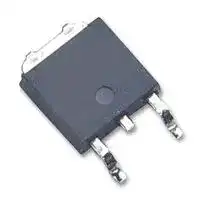
- Transistor Case Style: TO-252AA
- Drain Source Voltage Vds: 50V
- Operating Temperature Max: 150°C
- Continuous Drain Current Id: 16A
- Drain Source On State Resistance: 0.047ohm
- Gate Source Threshold Voltage Max: 2V
| Delivery and price | |
|---|---|
| Units per pack | 5000 |
| Price | 0.377 € |
| Current stock | 1000+ |
| Lead time | 30 days |
## RFD16N05LSM

## _Product Preview_ MOSFET - Power, N-Channel, Logic Level 50 V, 16 A, 47 m

These are N−Channel logic level power MOSFETs manufactured using the MegaFET process. This process, which uses feature sizes approaching those of LSI integrated circuits gives optimum utilization of silicon, resulting in outstanding performance. They were designed for use with logic level (5 V) driving sources in applications such as programmable controllers, switching regulators, switching converters, motor relay drivers and emitter switches for bipolar transistors. This performance is accomplished through a special gate oxide design which provides full rated conductance at gate biases in the 3 V to 5 V range, thereby facilitating true on−off power control directly from logic circuit supply voltages.

Formerly developmental type TA09871.

## **Features**

- 16 A, 50 V

- rDS(ON) = 0.047

- UIS SOA Rating Curve (Single Pulse)

- Design Optimized for 5 V Gate Drives

## **www.onsemi.com**

**==> picture [82 x 183] intentionally omitted <==**

**----- Start of picture text -----**<br>
D<br>G<br>S<br>D<br>G<br>2<br>S<br>DPAK<br>TO−252<br>CASE 369AS<br>**----- End of picture text -----**<br>


- Can be Driven Directly from CMOS, NMOS, TTL Circuits

- SOA is Power Dissipation Limited

## **MARKING DIAGRAM**

- Nanosecond Switching Speeds

- Linear Transfer Characteristics

- High Input Impedance

- Majority Carrier Device

- Related Literature

**==> picture [41 x 27] intentionally omitted <==**

**----- Start of picture text -----**<br>
$Y&Z&3&K<br>RFD16N<br>05LSM<br>**----- End of picture text -----**<br>


- ♦ TB334 “Guidelines for Soldering Surface Mount Components to PC Boards”

&Y = ON Semiconductor Logo &Z = Assembly Plant Code &3 = Numeric Date Code &K = Lot Code RFD16N05LSM = Specific Device Code

**ORDERING INFORMATION Part Number Package Brand** RFD16N05LSM9A TO−252AA RFD16N05LSM ~~——~~

Publication Order Number: **RFD16N05LSM/D**

**1**

© Semiconductor Components Industries, LLC, 2003 **May, 2019 − Rev. 2**

**RFD16N05LSM**

## **MAXIMUM RATINGS**

|**MAXIMUM RATINGS**||||
|---|---|---|---|
|**Rating**|**Symbol**|**RFD16N05LSM9A**|**Units**|
|Drain to Source Voltage (Note 1)|VDS|50|V|
|Drain to Gate Voltage (RGS20 k�) (Note 1)|VDGR|50|V|
|Continuous Drain Current|ID|16|A|
|Pulsed Drain Current (Note 3)|IDM|45|A|
|Gate to Source Voltage|VGS|±10|V|
|Maximum Power Dissipation|PD|60|W|
|Derate Above 25°C||0.48|W/°C|
|Operating and Storage Temperature|TJ, TSTG|−55 to 150|°C|
|Maximum Temperature for Soldering||||
|Leads at 0.063 in (1.6 mm) from Case for 10 s|TL|300|°C|
|Package Body for 10 s, See Techbrief 334|Tpkg|260|°C|


Stresses exceeding those listed in the Maximum Ratings table may damage the device. If any of these limits are exceeded, device functionality should not be assumed, damage may occur and reliability may be affected. 1. TJ = 25 ° C to 125 ° C.

## **ELECTRICAL SPECIFICATIONS** (TC = 25 ° C unless otherwise specified)

|**ELECTRICAL SPECIFICATIONS**(TC=|25°C unless|otherwise specified)|otherwise specified)|||||
|---|---|---|---|---|---|---|---|
|**PARAMETER**|**SYMBOL**|**TEST CONDITIONS**||**MIN**|**TYP**|**MAX**|**UNITS**|
|Drain to Source Breakdown Voltage|BVDSS|ID= 250 mA, VGS= 0 V, Figure 10||50|-|-|V|
|Gate to Threshold Voltage|VGS(TH)|VGS= VDS, ID= 250�A, Figure 9||1|−|2|V|
|Zero Gate Voltage Drain Current|IDSS|VDS= 40 V, VGS= 0 V<br>TC= 150°C||−|−|1|�A|
||||TC= 150°C|−|−|50|�A|
|Gate to Source Leakage Current|IGSS|VGS=±10 V, VDS= 0|V|−|−|100|nA|
|Drain to Source On Resistance (Note 2)|rDS(ON)|ID= 16 A, VGS= 5 V||−|−|0.047|�|
|||ID= 16 A, VGS= 4 V||−|−|0.056|�|
|Turn−On Time|t(ON)|VDD= 25 V, ID= 8 A, VGS =5 V,<br>RGS= 12.5�<br>Figures 15, 16||−|−|60|ns|
|Turn−On Delay Time|td(ON)|||−|14|−|ns|
|Rise Time|tr|||−|30|−|ns|
|Turn−Off Delay Time|td(OFF)|||−|42|−|ns|
|Fall Time|tf|||−|14|−|ns|
|Turn−Off Time|t(OFF)|||−|−|−|ns|
|Total Gate Charge|Qg(TOT)|VGS= 0 V to 10 V|VDD= 40 V,<br>ID= 16 A,<br>RL= 2.5Ω<br>Figures 17, 18|−|−|80|nC|
|Gate Charge at 5 V|Qg(5)|VGS= 0 V to 5 V||−|−|45|nC|
|Threshold Gate Charge|Qg(TH)|VGS= 0 V to 1 V||−|−|3|nC|
|Thermal Resistance Junction to Case|R�JC|||−|−|2.083|°C/W|
|Thermal Resistance Junction to Ambient|R�JA|||−|−|100|°C/W|


## **SOURCE TO DRAIN DIODE SPECIFICATIONS**

|**PARAMETER**|**SYMBOL**|**TEST CONDITIONS**|**MIN**|**TYP**|**MAX**|**UNITS**|
|---|---|---|---|---|---|---|
|Source to Drain Diode Voltage|VSD|ISD= 16 A|-|-|1.5|V|
|Diode Reverse Recovery Time|trr|ISD= 16 A, dISD/dt = 100 A/�s|-|-|125|ns|


2. Pulse Test: Pulse Width ≤ 300 ms, Duty Cycle ≤ 2 � .

3. Repetitive Rating: Pulse Width limited by max junction temperature.

**www.onsemi.com**

**2**

**RFD16N05LSM**

## **TYPICAL PERFORMANCE CURVES** (Unless Otherwise Specified)

**==> picture [485 x 613] intentionally omitted <==**

**----- Start of picture text -----**<br>
1.2 20<br>1.0<br>15<br>0.8<br>0.6 10<br>0.4<br>5<br>0.2<br>0 0<br>0 25 50 75 100 125 150 25 50 75 100 125 150<br>TC, CASE TEMPERATURE ( ° C) TC, CASE TEMPERATURE ( ° C)<br>Figure 1. Normalized Power Dissipation vs Figure 2. Maximum Continuous Drain Current<br>Case Temperature vs Case Temperature<br>10 [2] TC = 25 ° C 10 [2]<br>TJ = MAX RATED<br>ID MAX CONTINUOUS Idm Starting TJ = 25 ° C<br>Starting TJ = 150 ° C<br>OPERATION IN THIS AREA<br>LIMITED BY rDS(ON ) 10<br>1 DC<br>If R = 0<br>tAV = (L)(IAS)/(1.3 RATED BVDSS − VDD)<br>If R  ≠  0<br>tAV = (L/R)ln[(IAS  ×  R)/(1.3 RATED BVDSS − VDD) +1]<br>0.1 1<br>1 10 10 [2] 0.01 0.10 1 10<br>VDS, DRAIN TO SOURCE VOLTAGE (V) tAV, TIME IN AVALANCHE (ms)<br>Figure 3. Forward Bias Safe Operating Area Figure 4. Unclamped Inductive Switching SOA<br>(Single Pulse UIS SOA)<br>45 45<br>VGS = 10 V VGS = 4 V TC = 25 ° C VDS = 15 V<br>PULSE DURATION = 80 ms PULSE DURATION = 80 ms<br>DUTY CYCLE = 0.5% MAX. DUTY CYCLE = 0.5% MAX<br>30 VGS = 5 V 30<br>VGS = 3 V<br>15 15<br>VGS = 2 V<br>0 0<br>0 1.5 3.0 4.5 6.0 7.5 0 1.5 3.0 4.5 6.0<br>VDS, DRAIN TO SOURCE VOLTAGE (V) VGS, GATE TO SOURCE VOLTAGE (V)<br>, DRAIN CURRENT (A)<br>ID<br>POWER DISSIPATION MULTIPLIER<br>, DRAIN CURRENT (A)<br>ID , AVALANCHE CURRENT (A)<br>IAS<br>, DRAIN TO SOURCE CURRENT (A) , DRAIN TO SOURCE ON CURRENT (A)<br>IDS<br>IDS(ON)<br>**----- End of picture text -----**<br>


**Figure 5. Saturation Characteristics**

**Figure 6. Transfer Characteristics**

**www.onsemi.com**

**3**

**RFD16N05LSM**

## **TYPICAL PERFORMANCE CURVES** (Unless Otherwise Specified) (continued)

**==> picture [486 x 614] intentionally omitted <==**

**----- Start of picture text -----**<br>
1.4 2.5<br>ID = 16 V PULSE DURATION = 80  � s ID = 16 A<br>1.3 VDS = 15 V DUTY CYCLE = 0.5% MAX. PULSE DURATION = 80  � s<br>1.2 2.0 DUTY CYCLE = 0.5% MAX.<br>1.1<br>1.5<br>1.0<br>0.9<br>1.0<br>0.8<br>0.7<br>0.5<br>0.6<br>0.5 0<br>4 5 6 7 −50 0 50 100 150 200<br>VGS, GATE TO SOURCE VOLTAGE (V) TJ, JUNCTION TEMPERATURE ( ° C)<br>Figure 7. Drain to Source on Resitance vs Figure 8. Normalized Drain to Source on<br>Gate Voltageand Drain Current Resistance vs. Junction Temperature<br>1.4 1.4<br>ID = 250  � A ID = 250  � A<br>1.3 V GS  = V DS<br>1.2<br>1.2<br>1.1 1.0<br>1.0<br>0.9 0.8<br>0.8<br>0.6<br>0.7<br>0.6 0<br>−50 0 50 100 150 200 −50 0 50 100 150 200<br>TJ, JUNCTION TEMPERATURE ( ° C) TJ, JUNCTION TEMPERATURE ( ° C)<br>Figure 9. Normalized Gate Threshold vs Figure 10. Normalized Drain to Source<br>Junction Temperature Breakdown Voltage vs Junction Temperature<br>2000 50 RL = 3.125  � , VGS = 5 V<br>VGS = 0 V IG(REF) = 0.60 mA<br>f = 1 MHz<br>PLATEAU VOLTAGES IN DESCENDING ORDER:<br>1600<br>37.5 VDD = BVDSS VDD = BVDSS VDD = BVDSS<br>VDD = 0.75 BVDSS<br>1200 CISS VDD = 0.50 BVDSS<br>VDD = 0.25 BVDSS<br>CISS = CGS + CGD 25 GATE<br>800 CRSS = CGD SOURCE<br>COSS = CDS + CGD VOLTAGE<br>12.5<br>400 COSS<br>DRAIN TO SOURCE VOLTAGE<br>CRSS<br>0 0<br>0 5 10 15 20 25 0 I I<br>G(REF) G(REF)<br>20 80<br>VDS, DRAIN TO SOURCE VOLTAGE (V) IG(ACT) t, TIME ( � s) IG(ACT)<br>RESISTANCE ON RESISTANCE<br>NORMALIZED DRAIN TO SOURCEON  NORMALIZED DRAIN TO SOURCE<br>BREAKDOWN VOLTAGE<br>NORMALIZED DRAIN TO SOURCE<br>NORMALIZED GATE THRESHOLD VOLTAGE<br>C, CAPACITANCE (pF)<br>, DRAIN TO SOURCE VOLTAGE (V)<br>DS<br>V<br>**----- End of picture text -----**<br>


**Figure 11. Capacitance vs Drain to Source Voltage**

**Figure 12. Normalized Switching Waveforms for Constant Gate Current**

**www.onsemi.com**

**4**

**RFD16N05LSM**

## **TEST CIRCUITS AND WAVEFORMS**

**==> picture [226 x 148] intentionally omitted <==**

**----- Start of picture text -----**<br>
VDS<br>L<br>VARY tP TO OBTAIN +<br>REQUIRED PEAK I AS RG VDD<br>VGS −<br>DUT<br>tP<br>0 V IAS<br>0.01  �<br>**----- End of picture text -----**<br>


**==> picture [4 x 6] intentionally omitted <==**

**----- Start of picture text -----**<br>
0<br>**----- End of picture text -----**<br>


**==> picture [159 x 140] intentionally omitted <==**

**----- Start of picture text -----**<br>
BVDSS<br>tP<br>VDS<br>IAS<br>VDD<br>tAV<br>**----- End of picture text -----**<br>


**Figure 13. Unclamped Energy Test Circuit**

**Figure 14. Unclamped Energy Waveforms**

**==> picture [220 x 120] intentionally omitted <==**

**----- Start of picture text -----**<br>
RL<br>+<br>RG −VDD<br>DUT<br>VGS<br>**----- End of picture text -----**<br>


**==> picture [220 x 149] intentionally omitted <==**

**----- Start of picture text -----**<br>
tON tOFF<br>td(ON) td(OFF)<br>tr tf<br>VDS<br>90% 90%<br>10% 10%<br>0<br>90%<br>VGS 50% 50%<br>PULSE WIDTH<br>10%<br>0<br>**----- End of picture text -----**<br>


**Figure 15. Switching Time Test Circuit**

**Figure 16. Resistive Switching Waveforms**

**==> picture [470 x 184] intentionally omitted <==**

**----- Start of picture text -----**<br>
VDS<br>REGULATORCURRENT SUPPLY)(ISOL ATED VDD<br>Qg(TOT)<br>VGS<br>SAME TYPE Qgd<br>12V AS DUT<br>BATTERY 0.2  � F 50 k � Qgs<br>0.3  � F<br>D VDS<br>0<br>G DUT<br>IG(RE F) S IG(REF)<br>0<br>VDS<br>IG CURRENT ID CURRENT 0<br>SAMPLING SAMPLING<br>RESISTOR RESISTOR<br>**----- End of picture text -----**<br>


**Figure 17. Gate Charge Test Circuit**

**Figure 18. Gate Charge Waveforms**

**www.onsemi.com**

**5**

**RFD16N05LSM**

## **PSPICE ELECTRICAL MODEL**

.SUBCKT RFD16N05L 2 1 3 ; REV 4/8/92

Ca 12 8 3.33e-9 Cb 15 14 3.11e-9 Cin 6 8 1.21e-9 Dbody 7 5 DBDMOD Dbreak 5 11 DBKMOD Dplcap 10 5 DPLCAPMOD Ebreak 11 7 17 18 70.9 Eds 14 8 5 8 1 Egs 13 8 6 8 1 Esg 6 10 6 8 1 Evto 20 6 18 8 1

IT 8 17 1

Lgate 1 9 1.38e-9 Ldrain 2 5 1.0e-12 Lsource 3 7 1.0e-9 Mos1 16 6 8 8 MOSMOD M = 0.99 Mos2 16 21 8 8 MOSMOD M = 0.01

Rin 6 8 1e9 Rbreak 17 18 RBKMOD 1 Rdrain 5 16 RDSMOD 27.38e-3 Rgate 9 20 2.98 Rsource 8 7 RDSMOD 0.614e-3 Rvto 18 19 RVTOMOD 1

S1a 6 12 13 8 S1AMOD S1b 13 12 13 8 S1BMOD S2a 6 15 14 13 S2AMOD S2b 13 15 14 13 S2BMOD

Vbat 8 19 DC 1 Vto 21 6 0.448

.MODEL DBDMOD D (IS = 1.34e-13 RS = 1.21e-2 TRS1 = 1.64e-3 TRS2 = 2.59e-6 +CJO = 1.13e-9 TT = 4.14e-8) .MODEL DBKMOD D (RS = 8.82e-2 TRS1 = -2.01e-3 TRS2 = 7.32e-10) .MODEL DPLCAPMOD D (CJO = 0.522e-9 IS = 1e-30 N = 10) .MODEL MOSMOD NMOS (VTO = 2.054 KP = 24.73 IS = 1e-30 N = 10 TOX = 1 L = 1u W = 1u) .MODEL RBKMOD RES (TC1 = 1.01e-3 TC2 = 5.21e-8) .MODEL RDSMOD RES (TC1 = 3.66e-3 TC2 = 1.46e-5) .MODEL RVTOMOD RES (TC1 = -1.81e-3 TC2 = 1.41e-6) .MODEL S1AMOD VSWITCH(RON = 1e-5 ROFF = 0.1 VON = -4.25 VOFF = -2.25) .MODEL S1BMOD VSWITCH(RON = 1e-5 ROFF = 0.1 VON = -2.25 VOFF = -4.25) .MODEL S2AMOD VSWITCH(RON = 1e-5 ROFF = 0.1 VON = -0.65 VOFF = 4.35) .MODEL S2BMOD VSWITCH(RON = 1e-5 ROFF = 0.1 VON = 4.35 VOFF = -0.65) .ENDS

NOTE: For further discussion of the PSPICE model, consult _A New PSPICE Sub−Circuit for the Power MOSFET Featuring Global Temperature Options_ ; written by William J. Hepp and C. Frank Wheatley.

**www.onsemi.com**

**6**

**RFD16N05LSM**

**==> picture [354 x 290] intentionally omitted <==**

**----- Start of picture text -----**<br>
DPLCAP 5 DRAIN<br>10 2<br>LDRAIN<br>RSCL1<br>RSCL2 + 51 DBREAK<br>5<br>ESCL<br>51<br>− 50<br>ESG 6 RDRAIN 11 + DBODY<br>8 17<br>+ VTO 16 EBREAK 18<br>+ −<br>MOS2<br>GATE EVTO 21<br>9 20 + 18 − 6<br>1 MOS1<br>8<br>LGATE RGATE<br>RIN CIN<br>RSOURCE LSOURCE<br>8 7<br>3<br>SOURCE<br>S1A S2A<br>12 13 14 15 RBREAK<br>17 18<br>8 13<br>S1B S2B RVTO<br>13<br>CA + CB 14 IT 19<br>6 + 5 VBAT<br>EGS 8 EDS − 8 +<br>−<br>**----- End of picture text -----**<br>


**Figure 19.**

**www.onsemi.com**

**7**

## MECHANICAL CASE OUTLINE **PACKAGE DIMENSIONS**

**==> picture [94 x 29] intentionally omitted <==**

**----- Start of picture text -----**<br>
DPAK3 (TO−252 3 LD)<br>CASE 369AS<br>ISSUE O<br>**----- End of picture text -----**<br>


**==> picture [80 x 8] intentionally omitted <==**

**----- Start of picture text -----**<br>
DATE 30 SEP 2016<br>**----- End of picture text -----**<br>


## **DOCUMENT NUMBER:**

## **DESCRIPTION:**

## **98AON13810G**

## **DPAK3 (TO−252 3 LD)**

Electronic versions are uncontrolled except when accessed directly from the Document Repository. Printed  versions are uncontrolled  except when stamped  “CONTROLLED COPY” in red.

## **PAGE 1 OF 1**

**onsemi** and                     are trademarks of Semiconductor Components Industries, LLC dba onsemi **onsemi** or its subsidiaries in the United States and/or other countries. **onsemi** reserves the right to make changes without further notice to any products herein. **onsemi** makes no warranty, representation or guarantee regarding the suitability of its products for any particular purpose, nor does **onsemi** assume any liability arising out of the application or use of any product or circuit, and specifically disclaims any and all liability, including without limitation special, consequential or incidental damages. **onsemi** does not convey any license under its patent rights nor the rights of others.

www.onsemi.com

© Semiconductor Components Industries, LLC, 2019

**onsemi** , , and other names, marks, and brands are registered and/or common law trademarks of Semiconductor Components Industries, LLC dba “ **onsemi** ” or its affiliates and/or subsidiaries in the United States and/or other countries. **onsemi** owns the rights to a number of patents, trademarks, copyrights, trade secrets, and other intellectual property. A listing of **onsemi** ’s product/patent coverage may be accessed at www.onsemi.com/site/pdf/Patent−Marking.pdf. **onsemi** reserves the right to make changes at any time to any products or information herein, without notice. The information herein is provided “as−is” and **onsemi** makes no warranty, representation or guarantee regarding the accuracy of the information, product features, availability, functionality, or suitability of its products for any particular purpose, nor does **onsemi** assume any liability arising out of the application or use of any product or circuit, and specifically disclaims any and all liability, including without limitation special, consequential or incidental damages. Buyer is responsible for its products and applications using **onsemi** products, including compliance with all laws, regulations and safety requirements or standards, regardless of any support or applications information provided by **onsemi** . “Typical” parameters which may be provided in **onsemi** data sheets and/or specifications can and do vary in different applications and actual performance may vary over time. All operating parameters, including “Typicals” must be validated for each customer application by customer’s technical experts. **onsemi** does not convey any license under any of its intellectual property rights nor the rights of others. **onsemi** products are not designed, intended, or authorized for use as a critical component in life support systems or any FDA Class 3 medical devices or medical devices with a same or similar classification in a foreign jurisdiction or any devices intended for implantation in the human body. Should Buyer purchase or use **onsemi** products for any such unintended or unauthorized application, Buyer shall indemnify and hold **onsemi** and its officers, employees, subsidiaries, affiliates, and distributors harmless against all claims, costs, damages, and expenses, and reasonable attorney fees arising out of, directly or indirectly, any claim of personal injury or death associated with such unintended or unauthorized use, even if such claim alleges that **onsemi** was negligent regarding the design or manufacture of the part. **onsemi** is an Equal Opportunity/Affirmative Action Employer. This literature is subject to all applicable copyright laws and is not for resale in any manner.

## **PUBLICATION ORDERING INFORMATION**

**LITERATURE FULFILLMENT** : **TECHNICAL SUPPORT Email Requests to:** orderlit@onsemi.com **North American Technical Support: Europe, Middle East and Africa Technical Support:** Voice Mail: 1 800−282−9855 Toll Free USA/Canada Phone: 00421 33 790 2910 **onsemi Website:** www.onsemi.com Phone: 011 421 33 790 2910 For additional information, please contact your local Sales Representative

◊

**==> picture [232 x 43] intentionally omitted <==**
Updated at April 29, 2026
onsemi is a premier global supplier of intelligent power and sensing technologies, driving disruptive innovations across the automotive, industrial, and cloud infrastructure markets. Recognized for their commitment to sustainability and reliable supply chains, the company accelerates advancements in vehicle electrification, industrial automation, and 5G networks by solving the industry's most complex design challenges. At the core of their portfolio is an industry-leading selection of discrete semiconductors. This extensive range features thousands of high-performance bipolar transistors, single and dual MOSFETs, and a comprehensive array of diodes, including Zener, Schottky, and fast-recovery rectifiers. Engineered for superior thermal performance and energy efficiency, these foundational components are critical for demanding power conversion, switching, and signal conditioning applications. Beyond essential discretes, onsemi provides a robust suite of advanced power management and circuit protection solutions. Their lineup includes intelligent power modules, single IGBTs, and transient voltage suppression (TVS) diodes designed to safeguard sensitive circuitry. Complimented by integrated passive filters, AC/DC LED driver ICs, and specialized sub-2.4GHz RF transceivers, onsemi equips engineers with the scalable, high-quality technologies needed to build a cleaner, smarter, and more connected world.
About Novapart
Novapart is a B2B electronic component broker specialising in stock shortages and cost reduction. We source hard-to-find parts and identify compliant alternatives across a catalogue of 420,000+ components from 500+ manufacturers.
Learn more →Stock Shortage Specialist
When a component is unavailable, discontinued or has an unacceptable lead time, we tap into our network of vetted European and Asian distributors to source what you need — without compromising on quality or traceability.
Request a quote →Compliant Alternatives
We identify pin-to-pin, electrically equivalent substitutes that meet the same certifications (RoHS, AEC-Q100, REACH) as your original specification — validated against datasheets, not just part numbers. Often at a lower cost.
BOM Analysis service →