


RFD12N06RLESM9A
Power MOSFET, N Channel, 60 V, 17 A, 0.063 ohm, TO-252 (DPAK), Surface Mount
- Manufacturer: ONSEMI
- Product type: Single MOSFETs
- Transistor Polarity:N Channel; Continuous Drain Current Id:17A; Drain Source Voltage Vds:60V; On Resistance Rds(on):0.07ohm; Rds(on) Test Voltage Vgs:10V; Threshold Voltage Vgs:3V; Power Dissipation Pd:
- MSL: MSL 1 - Unlimited
- SVHC: Lead (25-Jun-2025)
- No. of Pins: 3Pins
- Channel Type: N Channel
- Product Range: -
- Qualification: -
- Power Dissipation: 49W
- Transistor Mounting: Surface Mount
- Rds(on) Test Voltage: 10V
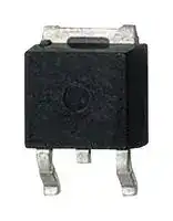
- Transistor Case Style: TO-252 (DPAK)
- Drain Source Voltage Vds: 60V
- Operating Temperature Max: 175°C
- Continuous Drain Current Id: 17A
- Drain Source On State Resistance: 0.063ohm
- Gate Source Threshold Voltage Max: 3V
| Delivery and price | |
|---|---|
| Units per pack | 1000 |
| Price | 0.399 € |
| Current stock | 100+ |
| Lead time | 30 days |
## **Is Now Part of**
## **To learn more about ON Semiconductor, please visit our website at www.onsemi.com**
Please note: As part of the Fairchild Semiconductor integration, some of the Fairchild orderable part numbers will need to change in order to meet ON Semiconductor’s system requirements. Since the ON Semiconductor product management systems do not have the ability to manage part nomenclature that utilizes an underscore (_), the underscore (_) in the Fairchild part numbers will be changed to a dash (-). This document may contain device numbers with an underscore (_). Please check the ON Semiconductor website to verify the updated device numbers. The most current and up-to-date ordering information can be found at www.onsemi.com. Please email any questions regarding the system integration to Fairchild_questions@onsemi.com.
ON Semiconductor and the ON Semiconductor logo are trademarks of Semiconductor Components Industries, LLC dba ON Semiconductor or its subsidiaries in the United States and/or other countries. ON Semiconductor owns the rights to a number of patents, trademarks, copyrights, trade secrets, and other intellectual property. A listing of ON Semiconductor’s product/patent coverage may be accessed at www.onsemi.com/site/pdf/Patent-Marking.pdf. ON Semiconductor reserves the right to make changes without further notice to any products herein. ON Semiconductor makes no warranty, representation or guarantee regarding the suitability of its products for any particular purpose, nor does ON Semiconductor assume any liability arising out of the application or use of any product or circuit, and specifically disclaims any and all liability, including without limitation special, consequential or incidental damages. Buyer is responsible for its products and applications using ON Semiconductor products, including compliance with all laws, regulations and safety requirements or standards, regardless of any support or applications information provided by ON Semiconductor. “Typical” parameters which may be provided in ON Semiconductor data sheets and/or specifications can and do vary in different applications and actual performance may vary over time. All operating parameters, including “Typicals” must be validated for each customer application by customer’s technical experts. ON Semiconductor does not convey any license under its patent rights nor the rights of others. ON Semiconductor products are not designed, intended, or authorized for use as a critical component in life support systems or any FDA Class 3 medical devices or medical devices with a same or similar classification in a foreign jurisdiction or any devices intended for implantation in the human body. Should Buyer purchase or use ON Semiconductor products for any such unintended or unauthorized application, Buyer shall indemnify and hold ON Semiconductor and its officers, employees, subsidiaries, affiliates, and distributors harmless against all claims, costs, damages, and expenses, and reasonable attorney fees arising out of, directly or indirectly, any claim of personal injury or death associated with such unintended or unauthorized use, even if such claim alleges that ON Semiconductor was negligent regarding the design or manufacture of the part. ON Semiconductor is an Equal Opportunity/Affirmative Action Employer. This literature is subject to all applicable copyright laws and is not for resale in any manner.
_**RFD12N06RLESM**_
## _**Data Sheet**_
## _**October 2013**_
## _**N-Channel UltraFET Power MOSFET**_
## _**60 V, 17 A, 71 mΩ**_
## _**Packaging**_
## _**Features**_
- Ultra Low On-Resistance
**==> picture [95 x 64] intentionally omitted <==**
**----- Start of picture text -----**<br>
JEDEC TO-252AA<br>DRAIN<br> (FLANGE)<br>GATE mma<br>SOURCE<br>**----- End of picture text -----**<br>
- rDS(ON) = 0.063Ω, VGS = 10V
- rDS(ON) = 0.071Ω, VGS = 5V
- Simulation Models
- Temperature Compensated PSPICE[®] and SABER[©] Electrical Models
- Spice and SABER[©] Thermal Impedance Models
- www.fairchildsemi.com
- Peak Current vs Pulse Width Curve
## _**Symbol**_
**==> picture [37 x 67] intentionally omitted <==**
**----- Start of picture text -----**<br>
D<br>G<br>S<br>**----- End of picture text -----**<br>
- UIS Rating Curve
- Switching Time vs RGS Curves
## _**Ordering Information**_
|**PART NUMBER**|**PACKAGE**|**BRAND**|
|---|---|---|
|RFD12N06RLESM9A|TO-252AA|12N6LE|
## **Absolute Maximum Ratings** TC = 25[o] C, Unless Otherwise Specified
||**RFD12N06RLESM9A**|**UNITS**|
|---|---|---|
|Drain to Source Voltage (Note 1) . . . . . . . . . . . . . . . . . . . . . . . . . . . . . . . . . . . . . VDSS|60|V|
|Drain to Gate Voltage (RGS= 20kΩ) (Note 1) . . . . . . . . . . . . . . . . . . . . . . . . . . VDGR|60|V|
|Gate to Source Voltage . . . . . . . . . . . . . . . . . . . . . . . . . . . . . . . . . . . . . . . . . . . . . VGS|±16|V|
|Drain Current|||
|Continuous (TC= 25oC, VGS= 5V) . . . . . . . . . . . . . . . . . . . . . . . . . . . . . . . . . . . . ID|17|A|
|Continuous (TC= 25oC, VGS= 10V) (Figure 2) . . . . . . . . . . . . . . . . . . . . . . . . . . .ID|18|A|
|Continuous (TC= 135oC, VGS= 5V) . . . . . . . . . . . . . . . . . . . . . . . . . . . . . . . . . . . ID|8|A|
|Continuous (TC= 135oC, VGS= 4.5V) (Figure 2) . . . . . . . . . . . . . . . . . . . . . . . . .ID|8|A|
|Pulsed Drain Current . . . . . . . . . . . . . . . . . . . . . . . . . . . . . . . . . . . . . . . . . . . . . IDM|Figure 4||
|Pulsed Avalanche Rating . . . . . . . . . . . . . . . . . . . . . . . . . . . . . . . . . . . . . . . . . . . UIS|Figures 6, 17, 18||
|Power Dissipation . . . . . . . . . . . . . . . . . . . . . . . . . . . . . . . . . . . . . . . . . . . . . . . . . . PD|49|W|
|Derate Above 25oC . . . . . . . . . . . . . . . . . . . . . . . . . . . . . . . . . . . . . . . . . . . . . . . . .|0.327|W/oC|
|Operating and Storage Temperature . . . . . . . . . . . . . . . . . . . . . . . . . . . . . . . TJ, TSTG|-55 to 175|oC|
|Maximum Temperature for Soldering|||
|Leads at 0.063in (1.6mm) from Case for 10s. . . . . . . . . . . . . . . . . . . . . . . . . . . . TL|300|oC|
|Package Body for 10s, See Techbrief TB334. . . . . . . . . . . . . . . . . . . . . . . . . . .Tpkg|260|oC|
|NOTE:|||
|1. TJ= 25oC to 150oC.|||
_**CAUTION:** Stresses above those listed in “Absolute Maximum Ratings” may cause permanent damage to the device. This is a stress only rating and operation of the device at these or any other conditions above those indicated in the operational sections of this specification is not implied._
©2002 Fairchild Semiconductor Corporation
RFD12N06RLESM9A Rev. C0
_**RFD12N06RLESM**_
## **Electrical Specifications** TC = 25[o] C, Unless Otherwise Specified
**PARAMETER SYMBOL TEST CONDITIONS MIN TYP MAX UNITS OFF STATE SPECIFICATIONS** Drain to Source Breakdown Voltage BVDSS ID = 250µA, VGS = 0V (Figure 12) 60 - - V ID = 250µA, VGS = 0V , TC = -40 ~~[o]~~ C (Figure 12) 55 - - V Zero Gate Voltage Drain Current IDSS VDS = 55V, VGS = 0V - - 1 µA VDS = 50V, VGS = 0V, TC = 150 ~~[o]~~ C - - 250 µA Gate to Source Leakage Current IGSS VGS = ±16V - - ±100 nA **ON STATE SPECIFICATIONS** Gate to Source Threshold Voltage VGS(TH) VGS = VDS, ID = 250µA (Figure 11) 1 - 3 V Drain to Source On Resistance rDS(ON) ID = 18A, VGS = 10V (Figures 9, 10) - 0.052 0.063 Ω ID = 8A, VGS = 5V (Figure 9) - 0.060 0.071 Ω ID = 8A, VGS = 4.5V (Figure 9) - 0.064 0.075 Ω **THERMAL SPECIFICATIONS** Thermal Resistance Junction to Case RθJC TO-252AA - - 3.06 ~~o~~ C/W Thermal Resistance Junction to RθJA - - 100 ~~o~~ C/W Ambient **SWITCHING SPECIFICATIONS** (VGS = 4.5V) Turn-On Time tON VDD = 30V, ID = 8A - - 153 ns ~~sie~~ Turn-On Delay Time td(ON) VGS = 4.5V, RGS = 22Ω - 13 - ns (Figures 15, 21, 22) Rise Time tr - 89 - ns Turn-Off Delay Time td(OFF) - 22 - ns Fall Time tf - 37 - ns Turn-Off Time tOFF - - 89 ns **SWITCHING SPECIFICATIONS** (VGS = 10V) Turn-On Time tON VDD = 30V, ID = 18A - - 59 ns ~~a5 f=isee~~ Turn-On Delay Time td(ON) RVGSGS = 24= 10V,Ω - 5.3 - ns Rise Time tr (Figures 16, 21, 22) - 34 - ns Turn-Off Delay Time td(OFF) - 41 - ns Fall Time tf - 50 - ns Turn-Off Time tOFF - - 136 ns ~~26 ES~~ **GATE CHARGE SPECIFICATIONS** Total Gate Charge Qg(TOT) VGS = 0V to 10V VDD = 30V, - 12 15 nC Gate Charge at 5V Threshold Gate Charge QQg(TH)g(5) VVGSGS = 0V to 5V = 0V to 1V I(Figures 14, 19, 20)IDg(REF) = 8A, = 1.0mA -- 0.546.8 0.658.2 nCnC Gate to Source Gate Charge Qgs - 1.7 - nC ~~=~~ Gate to Drain “Miller” Charge Qgd - 3 - nC **CAPACITANCE SPECIFICATIONS** Input Capacitance CISS VDS = 25V, VGS = 0V, - 485 - pF Output Capacitance COSS f = 1MHz - 130 - pF (Figure 13) Reverse Transfer Capacitance CRSS - 28 - pF ~~Sa~~ **Source to Drain Diode Specifications PARAMETER SYMBOL TEST CONDITIONS MIN TYP MAX UNITS** Source to Drain Diode Voltage VSD ISD = 8A - - 1.25 V ISD = 4A - - 1.0 V Reverse Recovery Time trr ISD = 8A, dISD/dt = 100A/µs - - 70 ns Reverse Recovered Charge QRR ISD = 8A, dISD/dt = 100A/µs - - 165 nC ~~SE~~
©2002 Fairchild Semiconductor Corporation
RFD12N06RLESM Rev. C0
_**RFD12N06RLESM**_
## _**Typical Performance Curves**_
**==> picture [510 x 605] intentionally omitted <==**
**----- Start of picture text -----**<br>
1.2 20<br>1.0<br>TTT TTTT) 15 6ATT TTT VGS = 10V<br>0.8<br>0.6 10 VGS = 4.5V<br>pt IN tt Su<br>0.4<br>INTN rw LN<br>5<br>0.2<br>0 pLtitiiinNn 0<br>0 25 50 75 100 125 150 175 25 50 75 100 125 150 175<br>coroeres = CLT<br>TC, CASE TEMPERATURE ( [o] C) TC, CASE TEMPERATURE ( [o] C)<br>FIGURE 1. NORMALIZED POWER DISSIPATION vs CASE FIGURE 2. MAXIMUM CONTINUOUS DRAIN CURRENT vs<br>TEMPERATURE CASE TEMPERATURE<br>2<br>DUTY CYCLE - DESCENDING ORDER<br>1 0.5<br>0.2<br>0.1<br>0.05<br>0.02<br>ae 0.01 eee<br>Seca o><br>PDM<br>0.1<br>ee<br>t1<br>t2<br>NOTES:<br>SINGLE PULSE DUTY FACTOR: D = t1/t2<br>PEAK TJ = PDM x Z θ JC x R θ JC + TC<br>0.01 a TT<br>wail EE PETE<br>10 [-5] 10 [-4] 10 [-3] 10 [-2] 10 [-1] 10 [0] 10 [1]<br>t, RECTANGULAR PULSE DURATION (s)<br>FIGURE 3. NORMALIZED MAXIMUM TRANSIENT THERMAL IMPEDANCE<br>200<br>TC = 25 [o] C<br>FOR TEMPERATURES<br>ABOVE 25 [o] C DERATE PEAK<br>100<br>CURRENT AS FOLLOWS:<br>ngs cee ones coe<br>PEE I = I 25 (——_ 175 - T C<br>150<br>PNT TTY PeTT | —— |<br>a a Ok<br>VGS = 5V<br>pt AT rt<br>TRANSCONDUCTANCE<br>MAY LIMIT CURRENT<br>IN THIS REGION<br>10<br>10 [-5] 10 [-4] 10 [-3] 10 [-2] 10 [-1] 10 [0] 10 [1]<br>t, PULSE WIDTH (s)<br>, DRAIN CURRENT (A)<br>ID<br>POWER DISSIPATION MULTIPLIER<br>, NORMALIZED<br>JC<br>θ<br>Z<br>THERMAL IMPEDANCE<br>, PEAK CURRENT (A)<br>IDM<br>**----- End of picture text -----**<br>
**FIGURE 4. PEAK CURRENT CAPABILITY**
©2002 Fairchild Semiconductor Corporation
RFD12N06RLESM Rev. C0
_**RFD12N06RLESM**_
## _**Typical Performance Curves**_ **(Continued)**
**==> picture [511 x 598] intentionally omitted <==**
**----- Start of picture text -----**<br>
60<br>100 If R = 0<br>tAV = (L)(IAS)/(1.3*RATED BVDSS - VDD)<br>If R ≠ 0<br>tAV = (L/R)ln[(IAS*R)/(1.3*RATED BVDSS - VDD) +1]<br>100 µ s<br>10<br>10<br>1ms STARTING TJ = 25 [o] C<br>OPERATION IN THIS<br>AREA MAY BE<br>1 LIMITED BY rDS(ON) 10ms<br>STARTING TJ = 150 [o] C<br>SSS Se a<br>SINGLE PULSE<br>TJ = MAX RATED TC = 25 [o] C<br>0.1 eee 1 CO SeSNOTa<br>0.01 0.1 1 10 100<br>1 10 100<br>VDS, DRAIN TO SOURCE VOLTAGE (V) tAV, TIME IN AVALANCHE (ms)<br>NOTE: Refer to Fairchild Application Notes AN9321 and AN9322.<br>FIGURE 5. FORWARD BIAS SAFE OPERATING AREA FIGURE 6. UNCLAMPED INDUCTIVE SWITCHING<br>CAPABILITY<br>20 20<br>PULSE DURATION = 80 µ s VGS = 10 V<br>DUTY CYCLE = 0.5% MAXVDD = 15V VGS = 5V V GS = 4V<br>15 15<br>V GS = 3.5V<br>10 10<br> TJ = 25 [o] C VGS = 3V<br>5 5<br>0 a TJ = 175 [o] C TJ = -55 [o] C T Y C | = 25 [o] C DUTY CYCLE = 0.5% MAXPULSE DURATION = 80 µ s<br>FF se e 0 An<br>1.0 2.0 3.0 4.0 5.0 0 1 2 3 4<br>VGS, GATE TO SOURCE VOLTAGE (V) VDS, DRAIN TO SOURCE VOLTAGE (V)<br>FIGURE 7. TRANSFER CHARACTERISTICS FIGURE 8. SATURATION CHARACTERISTICS<br>80 2.5<br>PULSE DURATION = 80 µ s PULSE DURATION = 80 µ s<br>DUTY CYCLE = 0.5% MAX DUTY CYCLE = 0.5% MAX<br>ID = 17A TC = 25 [o] C<br>70 No 2.0 i LLY<br>ID = 12A<br>ID = 7A<br>1.5<br>60<br>PRET ELE ee<br>1.0<br>50<br>PS C ET<br>VGS = 10V, ID = 18A<br>0.5<br>40 P|| fo) Lett<br>-80 -40 0 40 80 120 160 200<br>2 4 6 8 10<br>VGS, GATE TO SOURCE VOLTAGE (V) TJ, JUNCTION TEMPERATURE ( [o] C)<br>, DRAIN CURRENT (A)<br>ID , AVALANCHE CURRENT (A)<br>IAS<br> DRAIN CURRENT (A)ID, , DRAIN CURRENT (A)ID<br>) Ω<br>, DRAIN TO SOURCE<br>ON RESISTANCE<br>ON RESISTANCE (m<br>rDS(ON)<br>NORMALIZED DRAIN TO SOURCE<br>**----- End of picture text -----**<br>
**FIGURE 9. DRAIN TO SOURCE ON RESISTANCE vs GATE VOLTAGE AND DRAIN CURRENT**
**FIGURE 10. NORMALIZED DRAIN TO SOURCE ON RESISTANCE vs JUNCTION TEMPERATURE**
©2002 Fairchild Semiconductor Corporation
RFD12N06RLESM Rev. C0
_**RFD12N06RLESM**_
## _**Typical Performance Curves**_ **(Continued)**
**==> picture [234 x 598] intentionally omitted <==**
**----- Start of picture text -----**<br>
1.2<br>VGS = VDS, ID = 250 µ A<br>1.0<br>0.8<br>0.6<br>0.4<br>-80 -40 0 40 80 120 160 200<br>TJ, JUNCTION TEMPERATURE ( [o] C)<br>FIGURE 11. NORMALIZED GATE THRESHOLD VOLTAGE vs<br>JUNCTION TEMPERATURE<br>2000<br>1000 C ISS = C GS + C GD<br>100 COSS ≅ CDS + CGD<br>VGS = 0V, f = 1MHz CRSS = CGD<br>10<br>Pu CELEBS<br>0.1 1.0 10 60<br>VDS, DRAIN TO SOURCE VOLTAGE (V)<br>FIGURE 13. CAPACITANCE vs DRAIN TO SOURCE VOLTAGE<br>150<br>VGS = 4.5V, VDD = 30V, ID = 8A<br>120<br>yy | Up<br>tr<br>90<br>a ee<br>60 aa<br>tf<br>td(OFF)<br>|<br>30<br>td(ON)<br>0 SOT<br>0 10 20 30 40 50<br>RGS, GATE TO SOURCE RESISTANCE ( Ω )<br>NORMALIZED GATE<br>THRESHOLD VOLTAGE<br>C, CAPACITANCE (pF)<br>SWITCHING TIME (ns)<br>**----- End of picture text -----**<br>
**FIGURE 15. SWITCHING TIME vs GATE RESISTANCE**
**==> picture [234 x 374] intentionally omitted <==**
**----- Start of picture text -----**<br>
1.2<br>ID = 250 µ A<br>1.1<br>1.0<br>0.9<br>-80 -40 0 40 80 120 160 200<br>TJ, JUNCTION TEMPERATURE ( [o] C)<br>FIGURE 12. NORMALIZED DRAIN TO SOURCE BREAKDOWN<br>VOLTAGE vs JUNCTION TEMPERATURE<br>10<br>VDD = 30V<br>8<br>6<br>4<br>WAVEFORMS IN<br>DESCENDING ORDER:<br>2 ID = 17A<br>ID = 12A<br>ID = 7A<br>0<br>0 3 6 9 12 15<br>Qg, GATE CHARGE (nC)<br>BREAKDOWN VOLTAGE<br>NORMALIZED DRAIN TO SOURCE<br>, GATE TO SOURCE VOLTAGE (V)<br>GS<br>V<br>**----- End of picture text -----**<br>
**FIGURE 12. NORMALIZED DRAIN TO SOURCE BREAKDOWN VOLTAGE vs JUNCTION TEMPERATURE**
NOTE: Refer to Fairchild Application Notes AN7254 and AN7260.
**==> picture [226 x 17] intentionally omitted <==**
**----- Start of picture text -----**<br>
FIGURE 14. GATE CHARGE WAVEFORMS FOR CONSTANT<br>GATE CURRENT<br>**----- End of picture text -----**<br>
**==> picture [233 x 163] intentionally omitted <==**
**----- Start of picture text -----**<br>
100<br>VGS = 10V, VDD = 30V, ID = 18A<br>80<br>ae Al<br>60<br>tr<br>tf<br>40<br>aT td(OFF)<br>20<br>td(ON)<br>0 | |<br>po ff ff<br>0 10 20 30 40 50<br>RGS, GATE TO SOURCE RESISTANCE ( Ω )<br>SWITCHING TIME (ns)<br>**----- End of picture text -----**<br>
**FIGURE 16. SWITCHING TIME vs GATE RESISTANCE**
©2002 Fairchild Semiconductor Corporation
RFD12N06RLESM Rev. C0
_**RFD12N06RLESM**_
## _**Test Circuits and Waveforms**_
**==> picture [226 x 133] intentionally omitted <==**
**----- Start of picture text -----**<br>
VDS<br>L<br>VARY tP TO OBTAIN +<br>REQUIRED PEAK IAS RG —, VDD<br>VGS -<br>DUT<br>= ><br>tP<br>0V IAS<br>0.01 Ω<br>**----- End of picture text -----**<br>
**==> picture [215 x 130] intentionally omitted <==**
**----- Start of picture text -----**<br>
BVDSS<br><= tP —_<br>VDS<br>IAS an “h _—<br>—— VDD<br>7 / \<br>/ / \ \ A<br>/ \<br>4 \<br>y) 7 \<br>/ \<br>0<br>tAV<br>**----- End of picture text -----**<br>
**FIGURE 17. UNCLAMPED ENERGY TEST CIRCUIT**
**FIGURE 18. UNCLAMPED ENERGY WAVEFORMS**
**==> picture [522 x 153] intentionally omitted <==**
**----- Start of picture text -----**<br>
VDS<br>RL VDD Qg(TOT)<br>— e _—|-—______— GN ————+|<br>N XN VDS<br>s XN_— VGS = 10V<br>XN<br>VGS + I-——, Qg(5) —-+|<br>—— - VDD VGS —a N N nN VGS = 5V<br>N<br>DUT VGS = 1V N N<br>Ig(REF) 0 —_ |. Qg(TH)<br>Qgs Qgd<br>Ig(REF)<br>0<br>**----- End of picture text -----**<br>
**FIGURE 19. GATE CHARGE TEST CIRCUIT**
**FIGURE 20. GATE CHARGE WAVEFORMS**
**==> picture [495 x 145] intentionally omitted <==**
**----- Start of picture text -----**<br>
VDS — tON —_ > tOFF -_=_<br>_—_ td(ON) —> td(OFF)<br>RL —_—_ tr = —_—_ _ tf =<br>VDS<br>90% 90%<br>VGS +<br>VDD 10% 10%<br>- 0<br>DUT 90%<br>RGS<br>VGS 50% 50%<br>y o k <_— PULSE WIDTH ———“(3§©<br>VGS 0 10%<br>**----- End of picture text -----**<br>
**FIGURE 21. SWITCHING TIME TEST CIRCUIT**
**FIGURE 22. SWITCHING TIME WAVEFORM**
©2002 Fairchild Semiconductor Corporation
RFD12N06RLESM Rev. C0
_**RFD12N06RLESM**_
## _**PSPICE Electrical Model**_
.SUBCKT HUF76409D 2 1 3 ; rev 23 August 1999
CA 12 8 6.30e-10 CB 15 14 6.30e-10 CIN 6 8 4.60e-10
**==> picture [498 x 316] intentionally omitted <==**
**----- Start of picture text -----**<br>
DBODY 7 5 DBODYMOD<br>LDRAIN<br>DBREAK 5 11 DBREAKMOD<br>DPLCAP 5 DRAIN<br>DPLCAP 10 5 DPLCAPMOD<br>2<br>10<br>RLDRAIN<br>EBREAK 11 7 17 18 66.55 RSLC1<br>EDS 14 8 5 8 1 51 DBREAK<br>EGS 13 8 6 8 1 RSLC2<br>5<br>ESG 6 10 6 8 1 51 ESLC 11<br>EVTHRES 6 21 19 8 1<br>EVTEMP 20 6 18 22 1 - 50 +<br>ESG 6 RDRAIN EBREAK 1718 DBODY<br>IT 8 17 1 © + 8 EVTHRES 16 -<br>LDRAIN 2 5 1.00e-9 LGATE EVTEMP + 198 - 21 MWEAK<br>LGATE 1 9 3.73e-9 GATE RGATE + 18 - 6<br>LSOURCE 3 7 3.43e-9 1 22 MMED<br>9 20<br>MSTRO<br>MMED 16 6 8 8 MMEDMOD RLGATE<br>MSTRO 16 6 8 8 MSTROMOD LSOURCE<br>MWEAK 16 21 8 8 MWEAKMOD E CIN 8 . 7 SOURCE3<br>RBREAK 17 18 RBREAKMOD 1 RSOURCE<br>RLSOURCE<br>RDRAIN 50 16 RDRAINMOD 1.88e-2<br>RGATE 9 20 3.76 S1A S2A<br>RLDRAIN 2 5 10 12 13 14 15 RBREAK<br>17 18<br>RLGATE 1 9 37.3 8 13<br>RLSOURCE 3 7 34.3<br>S1B S2B RVTEMP<br>RSLC1 5 51 RSLCMOD 1e-6<br>RSLC2 5 50 1e3 CA 13 CB 19<br>RSOURCE 8 7 RSOURCEMOD 2.40e-2 + + 14 IT i e -<br>RVTHRES 22 8 RVTHRESMOD 1 6 5 VBAT<br>RVTEMP 18 19 RVTEMPMOD 1 EGS 8 EDS 8 +<br>- - 8<br>S1A 6 12 13 8 S1AMOD 22<br>S1B 13 12 13 8 S1BMOD<br>RVTHRES<br>+<br>-<br>**----- End of picture text -----**<br>
S1A 6 12 13 8 S1AMOD S1B 13 12 13 8 S1BMOD S2A 6 15 14 13 S2AMOD S2B 13 15 14 13 S2BMOD
## VBAT 22 19 DC 1
ESLC 51 50 VALUE={(V(5,51)/ABS(V(5,51)))*(PWR(V(5,51)/(1e-6*43),3))}
.MODEL DBODYMOD D (IS = 3.84e-13 RS = 1.56e-2 TRS1 = -1.0e-3 TRS2 = 7.0e-6 CJO = 6.4e-10 TT = 5.10e-8 XTI =4.35 M = 0.52) .MODEL DBREAKMOD D (RS = 3.70e- 1TRS1 = 9.10e- 4TRS2 = -1e-6) .MODEL DPLCAPMOD D (CJO = 3.70e-1 0IS = 1e-3 0N = 10 M = 0.79) .MODEL MMEDMOD NMOS (VTO = 2.08 KP = 3.2 IS = 1e-30 N = 10 TOX = 1 L = 1u W = 1u RG = 3.76) .MODEL MSTROMOD NMOS (VTO = 2.40 KP = 28 IS = 1e-30 N = 10 TOX = 1 L = 1u W = 1u) .MODEL MWEAKMOD NMOS (VTO = 1.80 KP = 0.08 IS = 1e-30 N = 10 TOX = 1 L = 1u W = 1u RG = 37.6 RS = 0.1) .MODEL RBREAKMOD RES (TC1 = 1.13e- 3TC2 = -3.00e-7) .MODEL RDRAINMOD RES (TC1 = 9.80e-3 TC2 = 2.85e-5) .MODEL RSLCMOD RES (TC1 = 5.00e-3 TC2 = 5.05e-6) .MODEL RSOURCEMOD RES (TC1 = 1.5e-3 TC2 = 1e-6) .MODEL RVTHRESMOD RES (TC1 = -1.48e-3 TC2 = -8.30e-6) .MODEL RVTEMPMOD RES (TC1 = -1.68e- 3TC2 = 8e-7)
.MODEL S1AMOD VSWITCH (RON = 1e-5 ROFF = 0.1 VON = -5 VOFF= -2.8) .MODEL S1BMOD VSWITCH (RON = 1e-5 ROFF = 0.1 VON = -2.8 VOFF= -5) .MODEL S2AMOD VSWITCH (RON = 1e-5 ROFF = 0.1 VON = -0.5 VOFF= 0.5) .MODEL S2BMOD VSWITCH (RON = 1e-5 ROFF = 0.1 VON = 0.5 VOFF= -0.5)
## .ENDS
NOTE: For further discussion of the PSPICE model, consult **A New PSPICE Sub-Circuit for the Power MOSFET Featuring Global Temperature Options** ; IEEE Power Electronics Specialist Conference Records, 1991, written by William J. Hepp and C. Frank Wheatley.
©2002 Fairchild Semiconductor Corporation
RFD12N06RLESM Rev. C0
_**RFD12N06RLESM**_
## _**SABER Electrical Model**_
REV 23 August 1999
template huf76409d n2,n1,n3 electrical n2,n1,n3 { var i iscl
d..model dbodymod = (is = 3.84e-13, cjo = 6.40e-10, tt = 5.10e-8, xti = 4.35, m = 0.52) d..model dbreakmod = ()
d..model dplcapmod = (cjo = 3.70e-10, is = 1e-30, m = 0.79)
m..model mmedmod = (type=_n, vto = 2.08, kp = 3.2, is = 1e-30, tox = 1)
**==> picture [508 x 308] intentionally omitted <==**
**----- Start of picture text -----**<br>
m..model mstrongmod = (type=_n, vto = 2.40, kp = 28, is = 1e-30, tox = 1)<br>m..model mweakmod = (type=_n, vto = 1.80, kp = 0.08, is = 1e-30, tox = 1) LDRAIN<br>sw_vcsp..model s1amod = (ron = 1e-5, roff = 0.1, von = -5, voff = -2.8) DPLCAP 5 DRAIN<br>sw_vcsp..model s1bmod = (ron =1e-5, roff = 0.1, von = -2.8, voff = -5) 2<br>sw_vcsp..model s2amod = (ron = 1e-5, roff = 0.1, von = -0.5, voff = 0.5) 10<br>sw_vcsp..model s2bmod = (ron = 1e-5, roff = 0.1, von = 0.5, voff = -0.5) RSLC1 RLDRAIN<br>51 RDBREAK<br>c.ca n12 n8 = 6.30e-10 RSLC2<br>c.cb n15 n14 = 6.30e-10 ISCL 72 RDBODY<br>c.cin n6 n8 = 4.60e-10<br>d.dbody n7 n71 = model=dbodymod - ai 50 DBREAK e<br>d.dbreak n72 n11 = model=dbreakmod ESG 6 RDRAIN 11 71<br>d.dplcap n10 n5 = model=dplcapmod + 8 EVTHRES 16<br>i.it n8 n17 = 1 LGATE EVTEMP + 198 - 21 MWEAK DBODY<br>l.ldrain n2 n5 = 1.00e-9l.lgate n1 n9 = 3.73e-9l.lsource n3 n7 = 3.43e-9 GATE1 RLGATE 9RGATE20+ 1822 - 6 MSTRO MMED EBREAK+17<br>m.mmed n16 n6 n8 n8 = model=mmedmod, l=1u, w=1u CIN ! 8 (-) -18 7 LSOURCE SOURCE3<br>m.mstrong n16 n6 n8 n8 = model=mstrongmod, l=1u, w=1u RSOURCE<br>m.mweak n16 n21 n8 n8 = model=mweakmod, l=1u, w=1u RLSOURCE<br>S1A S2A<br>res.rbreak n17 n18 = 1, tc1 = 1.13e-3, tc2 = -3.00e-7res.rdbody n71 n5 = 1.56e-2, tc1 = -1.0e-3, tc2 = 7.00e-6res.rdbody n71 n5 = 1.56e-2, tc1 = -1.0e-3, tc2 = 7.00e-6 12 138 1413 15 17 RBREAK 18<br>res.rdbreak n72 n5 = 3.70e-1, tc1 = 9.10e-4, tc2 = -1e-6<br>res.rdrain n50 n16 = 1.88e-2, tc1 = 9.80e-3, tc2 = 2.85e-5 S1B S2B RVTEMP<br>res.rgate n9 n20 = 3.76 13 CB 19<br>res.rldrain n2 n5 = 10res.rlgate n1 n9 = 37.3res.rlsource n3 n7 = 34.3res.rlgate n1 n9 = 37.3res.rlsource n3 n7 = 34.3res.rlsource n3 n7 = 34.3 CA EGS +68 EDS + 58 14 IT | +- VBAT<br>res.rslc1 n5 n51= 1e-6, tc1 = 5.00e-3, tc2 = 5.05e-6res.rslc2 n5 n50 = 1e3res.rslc2 n5 n50 = 1e3 CK - ) © - 8 +<br>22<br>res.rsource n8 n7 = 2.40e-2, tc1 = 1.5e-3, tc2 =1e-6 RVTHRES<br>**----- End of picture text -----**<br>
res.rbreak n17 n18 = 1, tc1 = 1.13e-3, tc2 = -3.00e-7res.rdbody n71 n5 = 1.56e-2, tc1 = -1.0e-3, tc2 = 7.00e-6res.rdbody n71 n5 = 1.56e-2, tc1 = -1.0e-3, tc2 = 7.00e-6 res.rdbreak n72 n5 = 3.70e-1, tc1 = 9.10e-4, tc2 = -1e-6 res.rdrain n50 n16 = 1.88e-2, tc1 = 9.80e-3, tc2 = 2.85e-5 res.rgate n9 n20 = 3.76 res.rldrain n2 n5 = 10res.rlgate n1 n9 = 37.3res.rlsource n3 n7 = 34.3res.rlgate n1 n9 = 37.3res.rlsource n3 n7 = 34.3res.rlsource n3 n7 = 34.3 res.rslc1 n5 n51= 1e-6, tc1 = 5.00e-3, tc2 = 5.05e-6res.rslc2 n5 n50 = 1e3res.rslc2 n5 n50 = 1e3 res.rsource n8 n7 = 2.40e-2, tc1 = 1.5e-3, tc2 =1e-6 res.rvtemp n18 n19 = 1, tc1 = -1.68e-3, tc2 = 8.00e-7 res.rvthres n22 n8 = 1, tc1 = -1.48e-3, tc2 = -8.30e-6
spe.ebreak n11 n7 n17 n18 = 66.55 spe.eds n14 n8 n5 n8 = 1 spe.egs n13 n8 n6 n8 = 1 spe.esg n6 n10 n6 n8 = 1 spe.evtemp n20 n6 n18 n22 = 1 spe.evthres n6 n21 n19 n8 = 1
sw_vcsp.s1a n6 n12 n13 n8 = model=s1amod sw_vcsp.s1b n13 n12 n13 n8 = model=s1bmod sw_vcsp.s2a n6 n15 n14 n13 = model=s2amod sw_vcsp.s2b n13 n15 n14 n13 = model=s2bmod
v.vbat n22 n19 = dc=1
equations { i (n51->n50) +=iscl iscl: v(n51,n50) = ((v(n5,n51)/(1e-9+abs(v(n5,n51))))*((abs(v(n5,n51)*1e6/43))** 3)) } }
©2002 Fairchild Semiconductor Corporation
RFD12N06RLESM Rev. C0
_**RFD12N06RLESM**_
## _**SPICE Thermal Model**_
REV 10 September 1999
## HUF76409T
CTHERM1 th 6 9.50e-4 CTHERM2 6 5 2.40e-3 CTHERM3 5 4 3.90e-3 CTHERM4 4 3 4.10e-3 CTHERM5 3 2 5.60e-3 CTHERM6 2 tl 4.00e-2
RTHERM1 th 6 2.00e-2 RTHERM2 6 5 1.10e-1 RTHERM3 5 4 2.75e-1 RTHERM4 4 3 5.53e-1 RTHERM5 3 2 7.25e-1 RTHERM6 2 tl 7.56e-1
## _**SABER Thermal Model**_
SABER thermal model HUF76409T
template thermal_model th tl thermal_c th, tl { ctherm.ctherm1 th 6 = 9.50e-4 ctherm.ctherm2 6 5 = 2.40e-3 ctherm.ctherm3 5 4 = 3.90e-3 ctherm.ctherm4 4 3 = 4.10e-3 ctherm.ctherm5 3 2 = 5.60e-3 ctherm.ctherm6 2 tl = 4.00e-2
rtherm.rtherm1 th 6 = 2.00e-2 rtherm.rtherm2 6 5 = 1.10e-1 rtherm.rtherm3 5 4 = 2.75e-1 rtherm.rtherm4 4 3 = 5.53e-1 rtherm.rtherm5 3 2 = 7.25e-1 rtherm.rtherm6 2 tl = 7.56e-1 }
**==> picture [160 x 489] intentionally omitted <==**
**----- Start of picture text -----**<br>
th JUNCTION<br>RTHERM1 CTHERM1<br>6<br>RTHERM2 CTHERM2<br>5<br>RTHERM3 CTHERM3<br>4<br>RTHERM4 CTHERM4<br>3<br>RTHERM5 CTHERM5<br>2<br>RTHERM6 CTHERM6<br>tl CASE<br>**----- End of picture text -----**<br>
©2002 Fairchild Semiconductor Corporation
RFD12N06RLESM Rev. C0
_**RFD12N06RLESM**_
## **TRADEMARKS**
The following includes registered and unregistered trademarks and service marks, owned by Fairchild Semiconductor and/or its global subsidiaries, and is not intended to be an exhaustive list of all such trademarks.
|AccuPower™<br>AX-CAP®*<br>BitSiC™<br>Build it Now™<br>CorePLUS™<br>CorePOWER™<br>_CROSSVOLT_™<br>CTL™<br>Current Transfer Logic™<br>DEUXPEED®<br>Dual Cool™<br>EcoSPARK®<br>EfficentMax™<br>ESBC™<br>Fairchild®<br>Fairchild Semiconductor®<br>FACT Quiet Series™<br>FACT®<br>FAST®<br>FastvCore™<br>FETBench™<br>FPS™<br>®|F-PFS™<br>FRFET®<br>Global Power ResourceSM<br>GreenBridge™<br>Green FPS™<br>Green FPS™ e-Series™<br>G_max_™<br>GTO™<br>IntelliMAX™<br>ISOPLANAR™<br>Marking Small Speakers Sound Louder<br>and Better™<br>MegaBuck™<br>MICROCOUPLER™<br>MicroFET™<br>MicroPak™<br>MicroPak2™<br>MillerDrive™<br>MotionMax™<br>mWSaver®<br>OptoHiT™<br>OPTOLOGIC®<br>OPTOPLANAR®|PowerTrench®<br>PowerXS™<br>Programmable Active Droop™<br>QFET®<br>QS™<br>Quiet Series™<br>RapidConfigure™<br>Saving our world, 1mW/W/kW at a time™<br>SignalWise™<br>SmartMax™<br>SMART START™<br>Solutions for Your Success™<br>SPM®<br>STEALTH™<br>SuperFET®<br>SuperSOT™-3<br>SuperSOT™-6<br>SuperSOT™-8<br>SupreMOS®<br>SyncFET™<br>™<br>tm®|Sync-Lock™<br>®*<br>TinyBoost®<br>TinyBuck®<br>TinyCalc™<br>TinyLogic®<br>TINYOPTO™<br>TinyPower™<br>TinyPWM™<br>TinyWire™<br>TranSiC™<br>TriFault Detect™<br>TRUECURRENT®*<br>SerDes™<br>UHC®<br>Ultra FRFET™<br>UniFET™<br>VCX™<br>VisualMax™<br>VoltagePlus™<br>XS™<br>E SYSTEM<br>GENERAL<br>WZ...|
|---|---|---|---|
*Trademarks of System General Corporation, used under license by Fairchild Semiconductor.
## **DISCLAIMER**
FAIRCHILD SEMICONDUCTOR RESERVES THE RIGHT TO MAKE CHANGES WITHOUT FURTHER NOTICE TO ANY PRODUCTS HEREIN TO IMPROVE RELIABILITY, FUNCTION, OR DESIGN. FAIRCHILD DOES NOT ASSUME ANY LIABILITY ARISING OUT OF THE APPLICATION OR USE OF ANY PRODUCT OR CIRCUIT DESCRIBED HEREIN; NEITHER DOES IT CONVEY ANY LICENSE UNDER ITS PATENT RIGHTS, NOR THE RIGHTS OF OTHERS. THESE SPECIFICATIONS DO NOT EXPAND THE TERMS OF FAIRCHILD’S WORLDWIDE TERMS AND CONDITIONS, SPECIFICALLY THE WARRANTY THEREIN, WHICH COVERS THESE PRODUCTS.
## **LIFE SUPPORT POLICY**
FAIRCHILD’S PRODUCTS ARE NOT AUTHORIZED FOR USE AS CRITICAL COMPONENTS IN LIFE SUPPORT DEVICES OR SYSTEMS WITHOUT THE EXPRESS WRITTEN APPROVAL OF FAIRCHILD SEMICONDUCTOR CORPORATION.
As used here in:
1. Life support devices or systems are devices or systems which, (a) are 2. A critical component in any component of a life support, device, or intended for surgical implant into the body or (b) support or sustain life, system whose failure to perform can be reasonably expected to cause and (c) whose failure to perform when properly used in accordance with the failure of the life support device or system, or to affect its safety or instructions for use provided in the labeling, can be reasonably effectiveness. expected to result in a significant injury of the user.
## **ANTI-COUNTERFEITING POLICY**
Fairchild Semiconductor Corporation’s Anti-Counterfeiting Policy. Fairchild’s Anti-Counterfeiting Policy is also stated on our external website, www.Fairchildsemi.com, under Sales Support.
Counterfeiting of semiconductor parts is a growing problem in the industry. All manufactures of semiconductor products are experiencing counterfeiting of their parts. Customers who inadvertently purchase counterfeit parts experience many problems such as loss of brand reputation, substandard performance, failed application, and increased cost of production and manufacturing delays. Fairchild is taking strong measures to protect ourselves and our customers from the proliferation of counterfeit parts. Fairchild strongly encourages customers to purchase Fairchild parts either directly from Fairchild or from Authorized Fairchild Distributors who are listed by country on our web page cited above. Products customers buy either from Fairchild directly or from Authorized Fairchild Distributors are genuine parts, have full traceability, meet Fairchild’s quality standards for handing and storage and provide access to Fairchild’s full range of up-to-date technical and product information. Fairchild and our Authorized Distributors will stand behind all warranties and will appropriately address and warranty issues that may arise. Fairchild will not provide any warranty coverage or other assistance for parts bought from Unauthorized Sources. Fairchild is committed to combat this global problem and encourage our customers to do their part in stopping this practice by buying direct or from authorized distributors.
## **PRODUCT STATUS DEFINITIONS**
## **Definition of Terms**
|**Datasheet Identification**|**Product Status**|**Definition**|
|---|---|---|
|Advance Information|Formative / In Design|Datasheet contains the design specifications for product development. Specifications<br>may change in any manner without notice.|
|Preliminary|First Production|Datasheet contains preliminary data; supplementary data will be published at a later<br>date. Fairchild Semiconductor reserves the right to make changes at any time without<br>notice to improve design.|
|No Identification Needed|Full Production|Datasheet contains final specifications. Fairchild Semiconductor reserves the right to<br>make changes at any time without notice to improve the design.|
|Obsolete|Not In Production|Datasheet contains specifications on a product that is discontinued by Fairchild<br>Semiconductor. The datasheet is for reference information only.|
Rev. I66
©2002 Fairchild Semiconductor Corporation
RFD12N06RLESM Rev. C0
ON Semiconductor and are trademarks of Semiconductor Components Industries, LLC dba ON Semiconductor or its subsidiaries in the United States and/or other countries. ON Semiconductor owns the rights to a number of patents, trademarks, copyrights, trade secrets, and other intellectual property. A listing of ON Semiconductor’s product/patent coverage may be accessed at www.onsemi.com/site/pdf/Patent−Marking.pdf. ON Semiconductor reserves the right to make changes without further notice to any products herein. ON Semiconductor makes no warranty, representation or guarantee regarding the suitability of its products for any particular purpose, nor does ON Semiconductor assume any liability arising out of the application or use of any product or circuit, and specifically disclaims any and all liability, including without limitation special, consequential or incidental damages. Buyer is responsible for its products and applications using ON Semiconductor products, including compliance with all laws, regulations and safety requirements or standards, regardless of any support or applications information provided by ON Semiconductor. “Typical” parameters which may be provided in ON Semiconductor data sheets and/or specifications can and do vary in different applications and actual performance may vary over time. All operating parameters, including “Typicals” must be validated for each customer application by customer’s technical experts. ON Semiconductor does not convey any license under its patent rights nor the rights of others. ON Semiconductor products are not designed, intended, or authorized for use as a critical component in life support systems or any FDA Class 3 medical devices or medical devices with a same or similar classification in a foreign jurisdiction or any devices intended for implantation in the human body. Should Buyer purchase or use ON Semiconductor products for any such unintended or unauthorized application, Buyer shall indemnify and hold ON Semiconductor and its officers, employees, subsidiaries, affiliates, and distributors harmless against all claims, costs, damages, and expenses, and reasonable attorney fees arising out of, directly or indirectly, any claim of personal injury or death associated with such unintended or unauthorized use, even if such claim alleges that ON Semiconductor was negligent regarding the design or manufacture of the part. ON Semiconductor is an Equal Opportunity/Affirmative Action Employer. This literature is subject to all applicable copyright laws and is not for resale in any manner.
## **PUBLICATION ORDERING INFORMATION**
**N. American Technical Support** : 800−282−9855 Toll Free **ON Semiconductor Website** : **www.onsemi.com** USA/Canada
## **LITERATURE FULFILLMENT** :
Literature Distribution Center for ON Semiconductor
**Order Literature** : http://www.onsemi.com/orderlit For additional information, please contact your local Sales Representative
19521 E. 32nd Pkwy, Aurora, Colorado 80011 USA **Europe, Middle East and Africa Technical Support: Phone** : 303−675−2175 or 800−344−3860 Toll Free USA/Canada Phone: 421 33 790 2910 **Fax** : 303−675−2176 or 800−344−3867 Toll Free USA/Canada **Japan Customer Focus Center Email** : orderlit@onsemi.com Phone: 81−3−5817−1050
© Semiconductor Components Industries, LLC
www.onsemi.com
**www.onsemi.com**
**1**
Updated at April 29, 2026
onsemi is a premier global supplier of intelligent power and sensing technologies, driving disruptive innovations across the automotive, industrial, and cloud infrastructure markets. Recognized for their commitment to sustainability and reliable supply chains, the company accelerates advancements in vehicle electrification, industrial automation, and 5G networks by solving the industry's most complex design challenges. At the core of their portfolio is an industry-leading selection of discrete semiconductors. This extensive range features thousands of high-performance bipolar transistors, single and dual MOSFETs, and a comprehensive array of diodes, including Zener, Schottky, and fast-recovery rectifiers. Engineered for superior thermal performance and energy efficiency, these foundational components are critical for demanding power conversion, switching, and signal conditioning applications. Beyond essential discretes, onsemi provides a robust suite of advanced power management and circuit protection solutions. Their lineup includes intelligent power modules, single IGBTs, and transient voltage suppression (TVS) diodes designed to safeguard sensitive circuitry. Complimented by integrated passive filters, AC/DC LED driver ICs, and specialized sub-2.4GHz RF transceivers, onsemi equips engineers with the scalable, high-quality technologies needed to build a cleaner, smarter, and more connected world.
About Novapart
Novapart is a B2B electronic component broker specialising in stock shortages and cost reduction. We source hard-to-find parts and identify compliant alternatives across a catalogue of 420,000+ components from 500+ manufacturers.
Learn more →Stock Shortage Specialist
When a component is unavailable, discontinued or has an unacceptable lead time, we tap into our network of vetted European and Asian distributors to source what you need — without compromising on quality or traceability.
Request a quote →Compliant Alternatives
We identify pin-to-pin, electrically equivalent substitutes that meet the same certifications (RoHS, AEC-Q100, REACH) as your original specification — validated against datasheets, not just part numbers. Often at a lower cost.
BOM Analysis service →