
Image not available
Illustrative purposes only

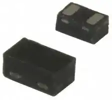
RCLAMP0521P.TCT
TVS DIODE ARRAY, 100W, 5V SLP1006P2
⚠️ Reference pricing provided. In case of supply shortages, we will connect you with our trusted procurement partners to ensure your project's continuity.
- Manufacturer: SEMTECH
- Product type: TVS Diodes
- Product Range:RailClamp Series; TVS Polarity:Bidirectional; Reverse Standoff Voltage:5V; Clamping Voltage Max:25V; Diode Case Style:SLP1006P2; No. of Pins:2Pins; M 10R1033
- No. of Pins: 2Pins
- TVS Polarity: Bidirectional
- Qualification: -
- Diode Mounting: Surface Mount
- Diode Case Style: SLP1006P2
- Clamping Voltage Max: 25V
- Reverse Standoff Voltage: 5V
- Maximum Breakdown Voltage: 11V
- Minimum Breakdown Voltage: 6V
- Operating Temperature Max: 125°C
- Peak Pulse Power Dissipation: 100W
| Delivery and price | |
|---|---|
| Units per pack | 3000 |
| Price | 0.288 € |
| Current stock | 25+ |
| Lead time | 30 days |
Datasheet

RClamp0521P Ultra-Low Capacitance 1-Line ESD protection PRELIMINARY

## **PROTECTION PRODUCTS** - RailClamp **[®]**

## Description

RailClamp[®] TVS arrays are ultra low capacitance ESD protection devices designed to protect high speed data interfaces. This series has been specifically designed to protect sensitive components which are connected to high-speed data and transmission lines from overvoltage caused by ESD (electrostatic discharge), CDE (Cable Discharge Events), and EFT (electrical fast transients).

The RClamp[®] 0521P has a maximum capacitance of only 0.50pF.  This allows it to be used on circuits operating in excess of 3GHz without signal attenuation.  They may be used to meet the ESD immunity requirements of IEC 61000-4-2, Level 4 (±15kV air, ±8kV contact discharge).

The RClamp0521P is in a 2-pin SLP1006P2 package measuring 1.0 x 0.6 x 0.5mm.  The leads are spaced at a pitch of 0.65mm and feature a lead-free finish. Each device will protect one high-speed line operating at 5 volts.  It gives the designer the flexibility to protect single lines in applications where arrays are not practical.  The combination of small size, low capacitance, and high ESD surge capability makes them ideal for use in applications such as cellular phones and digital video interfaces.

## Features

- Transient protection for data lines to IEC 61000-4-2 (ESD) ±15kV (air), ±8kV (contact) IEC 61000-4-4 (EFT) 40A (tp = 5/50ns) Cable Discharge Event (CDE)

- Ultra-small package (1.0 x 0.6 x 0.5mm)

- Protects one data or I/O line

- Low capacitance: 0.5pF

- Low clamping voltage

- Low operating voltage: 5.0V

- Solid-state silicon-avalanche technology

## Mechanical Characteristics

- SLP1006P2 package

- Molding compound flammability rating: UL 94V-0

- Marking: Marking code

- Packaging: Tape and Reel

- Lead Finish: NiPdAu

- Pb-Free, Halogen Free, RoHS/WEEE Compliant

## Applications

- Cellular Handsets & Accessories

- Digital Visual Interface (DVI)

- Display Port

- MDDI Ports

- USB Ports

- PCI Express

- Serial ATA

**==> picture [265 x 233] intentionally omitted <==**

**----- Start of picture text -----**<br>
Dimensions<br>1.0<br>0.60<br>0.65<br>0.50<br>Nominal Dimensions  (mm)<br>**----- End of picture text -----**<br>


## Schematic & Pin Configuration

**==> picture [265 x 209] intentionally omitted <==**

**----- Start of picture text -----**<br>
SLP1006P2  (Bottom View)<br>**----- End of picture text -----**<br>


www.semtech.com

Revision 5/18/2012

1

RClamp0521P

PRELIMINARY

|PRELIMINARY<br>PROTECTION PRODUCTS|PRELIMINARY<br>PROTECTION PRODUCTS|PRELIMINARY<br>PROTECTION PRODUCTS|PRELIMINARY<br>PROTECTION PRODUCTS|
|---|---|---|---|
|Absolute Maximum Rating||||
|||||
|g<br>n<br>it<br>a<br>R|l<br>o<br>b<br>m<br>y<br>S|e<br>ul<br>a<br>V|s<br>ti<br>n<br>U|
|)s<br>μ<br>0<br>2<br>/<br>8<br>=<br>p<br>t(<br>r<br>e<br>w<br>o<br>P<br>e<br>slu<br>P<br>k<br>a<br>e<br>P|P k<br>p|0<br>0<br>1|stt<br>a<br>W|
|(<br>t<br>n<br>e<br>rr<br>u<br>C<br>e<br>slu<br>P<br>k<br>a<br>e<br>P<br>m<br>u<br>m<br>ix<br>a<br>M<br>)s<br>μ<br>0<br>2<br>/<br>8<br>=<br>p<br>t|I p<br>p|4|s<br>p<br>m<br>A|
|)riA<br>(<br>2<br>-<br>4<br>-<br>0<br>0<br>0<br>1<br>6<br>C<br>EI<br>r<br>e<br>p<br>D<br>S<br>E<br>)tc<br>a<br>t<br>n<br>o<br>C<br>(<br>2<br>-<br>4<br>-<br>0<br>0<br>0<br>1<br>6<br>C<br>EI<br>r<br>e<br>p<br>D<br>S<br>E|V<br>D<br>S<br>E|5<br>1<br>-/<br>+<br>8<br>-/<br>+|V<br>k|
|e<br>r<br>u<br>t<br>a<br>r<br>e<br>p<br>m<br>e<br>T<br>g<br>nit<br>a<br>r<br>e<br>p<br>O|TJ|5<br>2<br>1<br>+<br>o<br>t<br>5<br>5<br>-|C<br>°|
|e<br>r<br>u<br>t<br>a<br>r<br>e<br>p<br>m<br>e<br>T<br>e<br>g<br>a<br>r<br>o<br>t<br>S|T<br>G<br>T<br>S|0<br>5<br>1<br>+<br>o<br>t<br>5<br>5<br>-|C<br>°|


## Electrical Characteristics (T=25[o] C)

||||||||
|---|---|---|---|---|---|---|
|r<br>e<br>t<br>e<br>m<br>a<br>r<br>a<br>P|l<br>o<br>b<br>m<br>y<br>S|s<br>n<br>oiti<br>d<br>n<br>o<br>C|m<br>u<br>m<br>i<br>ni<br>M|l<br>a<br>ci<br>p<br>y<br>T|m<br>u<br>m<br>ix<br>a<br>M|s<br>ti<br>n<br>U|
|e<br>g<br>a<br>tlo<br>V<br>ff<br>O<br>-<br>d<br>n<br>a<br>t<br>S<br>e<br>sr<br>e<br>v<br>e<br>R|V<br>M<br>W<br>R||||5|V|
|e<br>g<br>a<br>tlo<br>V<br>n<br>w<br>o<br>d<br>k<br>a<br>e<br>r<br>B<br>e<br>sr<br>e<br>v<br>e<br>R|V R<br>B|It<br>A<br>m<br>1<br>=|6|3<br>.<br>9|1<br>1|V|
|t<br>n<br>e<br>rr<br>u<br>C<br>e<br>g<br>a<br>k<br>a<br>e<br>L<br>e<br>sr<br>e<br>v<br>e<br>R|IR|V<br>M<br>W<br>R<br>C<br>°<br>5<br>2<br>=<br>T<br>,V<br>5<br>=||5<br>2<br>0<br>.<br>0|1|A<br>μ|
|e<br>g<br>a<br>tlo<br>V<br>g<br>nip<br>m<br>alC|VC|I P<br>P<br>s<br>μ<br>0<br>2<br>/<br>8<br>=<br>p<br>t<br>,<br>A<br>1<br>=|||5<br>1|V|
|e<br>g<br>a<br>tlo<br>V<br>g<br>nip<br>m<br>alC|VC|I P<br>P<br>s<br>μ<br>0<br>2<br>/<br>8<br>=<br>p<br>t<br>,<br>A<br>4<br>=|||5<br>2|V|
|e<br>c<br>n<br>a<br>tic<br>a<br>p<br>a<br>C<br>n<br>oitc<br>n<br>u<br>J|Cj|VR<br>z<br>H<br>M<br>1<br>=<br>f<br>,V<br>0<br>=||0<br>3<br>.<br>0|0<br>5<br>.<br>0|F<br>p|


www.semtech.com

© 2012 Semtech Corporation

2

RClamp0521P

PRELIMINARY

PROTECTION PRODUCTS

## Typical Characteristics

Non-Repetitive Peak Pulse Power vs. Pulse Time

**==> picture [264 x 177] intentionally omitted <==**

**----- Start of picture text -----**<br>
10<br>1<br>0.1<br>DR040412-100<br>0.01<br>0.1 1 10 100 1000<br>Pulse Duration - tp (µs)<br> (kW)<br>PP<br>Peak Pulse Power - P<br>**----- End of picture text -----**<br>


## Clamping Voltage vs. Peak Pulse Current

**==> picture [263 x 179] intentionally omitted <==**

**----- Start of picture text -----**<br>
25<br>20<br>15<br>10<br>5 Waveform<br> Parameters:<br>tr = 8µs<br>td = 20µs<br>0<br>0 1 2 3 4 5<br>Peak Pulse Current - IPP (A)<br> (V)<br>C<br>Clamping Voltage - V<br>**----- End of picture text -----**<br>


## Normalized Capacitance vs. Reverse Voltage

**==> picture [265 x 176] intentionally omitted <==**

**----- Start of picture text -----**<br>
2<br>f = 1 MHz<br>1.5<br>1<br>0.5<br>0<br>0 1 2 3 4 5<br>Reverse Voltage - VR (V)<br>=0)<br>R<br>) / C(VJ<br>R<br>C(VJ<br>**----- End of picture text -----**<br>


## Power Derating Curve

**==> picture [263 x 176] intentionally omitted <==**

**----- Start of picture text -----**<br>
120<br>100<br>80<br>60<br>40<br>20<br>DR040512:25:125:150<br>0<br>0 25 50 75 100 125 150<br>Ambient Temperature - TA ( [O] C)<br>PP<br>% of Rated Power or I<br>**----- End of picture text -----**<br>


## TLP Characteristic (Positive Pulse)

**==> picture [261 x 174] intentionally omitted <==**

**----- Start of picture text -----**<br>
30<br>25<br>RDYN = 0.90 Ohms<br>20<br>15<br>10<br>TLP<br>5  Parameters:<br>tp = 100ns<br>tr = 200ps<br>0<br>0 10 20 30 40 50<br>TLP Voltage (V)<br>TLP Current (A)<br>**----- End of picture text -----**<br>


## Typical Insertion Loss (S21)

**==> picture [239 x 193] intentionally omitted <==**

**----- Start of picture text -----**<br>
CH1 S21 LOG 6 dB / REF 0 dB<br>1: - .07980 dB<br>900 MHz<br> 0 dB  4 2: - .04580 dB 1.0 GHz<br>1 2 3<br>-6 dB  3: - .12250 dB<br>1.8 GHz<br> -12 dB<br>4: - .33470 dB<br>    2.5 GHz<br> -18 dB<br> -24 dB<br> -30 dB<br> -36 dB<br> -42 dB<br> -48 dB<br>1  10  100  1  3<br> MHz   MHz  MHz  GHz  GHz<br>START. 030 MHz STOP 3000.000000 MHz<br>**----- End of picture text -----**<br>


www.semtech.com

© 2012 Semtech Corporation

3

RClamp0521P

PROTECTION PRODUCTS

**==> picture [85 x 11] intentionally omitted <==**

**----- Start of picture text -----**<br>
PRELIMINARY<br>**----- End of picture text -----**<br>


## Typical Characteristics

## ESD Clamping (+8kV Contact per IEC 61000-4-2)

## ESD Clamping (-8kV Contact per IEC 61000-4-2)

**==> picture [533 x 174] intentionally omitted <==**

**----- Start of picture text -----**<br>
35 5<br>TA = 25oC<br>30 Corrected for 20dB attenuation 0<br>Measured with 50Ω, 20dB attenuator<br>50Ω Scope input impedance -5<br>25<br>-10<br>20<br>-15<br>15<br>-20<br>10<br>-25 T A  = 25 [o] C<br>Corrected for 20dB attenuation<br>5 -30 Measured with 50Ω, 20dB attenuator<br>50Ω Scope input impedance<br>0 -35<br>-10 0 10 20 30 40 50 60 -10 0 10 20 30 40 50 60<br>Time (ns) Time (ns)<br>Voltage (V) Voltage (V)<br>**----- End of picture text -----**<br>


## Applications Information

## Device Connection Options

## Equivalent Circuit Diagram

These low capacitance TVS diodes are designed to provide common mode protection for one high-speed line or differential protection for one line pair.  The device is bidirectional and may be used on lines where the signal polarity is positive and negative.

## Circuit Board Layout Recommendations for Suppression of ESD.

Good circuit board layout is critical for the suppression of ESD induced transients.  The following guidelines are recommended:

- Place the TVS near the input terminals or connectors to restrict transient coupling.

- Minimize the path length between the TVS and the protected line.

- Minimize all conductive loops including power and ground loops.

- The ESD transient return path to ground should be kept as short as possible.

- Never run critical signals near board edges.

- Use ground planes whenever possible.

www.semtech.com

4

© 2012 Semtech Corporation

RClamp0521P

## PROTECTION PRODUCTS Applications Information - Spice Model

**==> picture [85 x 10] intentionally omitted <==**

**----- Start of picture text -----**<br>
PRELIMINARY<br>**----- End of picture text -----**<br>


**==> picture [41 x 10] intentionally omitted <==**

**----- Start of picture text -----**<br>
I/O Line<br>**----- End of picture text -----**<br>


RClamp0521P Spice Model

|s<br>r<br>e<br>t<br>e<br>m<br>a<br>r<br>a<br>P<br>e<br>ci<br>p<br>S<br>P<br>1<br>2<br>5<br>0<br>p<br>m<br>al<br>C<br>R|s<br>r<br>e<br>t<br>e<br>m<br>a<br>r<br>a<br>P<br>e<br>ci<br>p<br>S<br>P<br>1<br>2<br>5<br>0<br>p<br>m<br>al<br>C<br>R|s<br>r<br>e<br>t<br>e<br>m<br>a<br>r<br>a<br>P<br>e<br>ci<br>p<br>S<br>P<br>1<br>2<br>5<br>0<br>p<br>m<br>al<br>C<br>R|s<br>r<br>e<br>t<br>e<br>m<br>a<br>r<br>a<br>P<br>e<br>ci<br>p<br>S<br>P<br>1<br>2<br>5<br>0<br>p<br>m<br>al<br>C<br>R|s<br>r<br>e<br>t<br>e<br>m<br>a<br>r<br>a<br>P<br>e<br>ci<br>p<br>S<br>P<br>1<br>2<br>5<br>0<br>p<br>m<br>al<br>C<br>R|
|---|---|---|---|---|
|r<br>e<br>t<br>e<br>m<br>a<br>r<br>a<br>P|ti<br>n<br>U|)<br>D<br>R<br>C<br>L<br>(<br>1<br>D|)<br>D<br>R<br>C<br>L<br>(<br>2<br>D|)<br>S<br>V<br>T<br>(<br>3<br>D|
|S<br>I|p<br>m<br>A|0<br>2<br>-<br>E<br>0<br>.<br>1|0<br>2<br>-<br>E<br>0<br>.<br>1|2<br>1<br>-<br>E<br>0<br>.<br>2|
|V<br>B|tlo<br>V|0<br>0<br>1|0<br>0<br>1|6<br>3<br>.<br>9|
|J<br>V|tlo<br>V|7<br>.<br>0|7<br>.<br>0|6<br>.<br>0|
|S<br>R|m<br>h<br>O|8<br>5<br>4<br>.<br>0|9<br>8<br>.<br>0|8<br>.<br>0|
|V<br>B<br>I|p<br>m<br>A|3<br>-<br>E<br>1|3<br>-<br>E<br>1|3<br>-<br>E<br>1|
|O<br>J<br>C|d<br>a<br>r<br>a<br>F|2<br>1<br>-<br>E<br>4<br>.<br>0|2<br>1<br>-<br>E<br>4<br>.<br>0|2<br>1<br>-<br>E<br>6<br>5|
|T<br>T|c<br>e<br>s|9<br>-<br>E<br>1<br>4<br>5<br>.<br>2|9<br>-<br>E<br>1<br>4<br>5<br>.<br>2|9<br>-<br>E<br>1<br>4<br>5<br>.<br>2|
|M|--|1<br>0<br>.<br>0|1<br>0<br>.<br>0|3<br>2<br>.<br>0|
|N|--|1.<br>1|1.<br>1|1.<br>1|
|G<br>E|V<br>e|1<br>1.<br>1|1<br>1.<br>1|1<br>1.<br>1|


www.semtech.com

© 2012 Semtech Corporation

5

RClamp0521P

PRELIMINARY

## PROTECTION PRODUCTS

## Outline Drawing - SO-8Outline Drawing - SLP1006P2

**==> picture [372 x 278] intentionally omitted <==**

**----- Start of picture text -----**<br>
B<br>A D<br>DIMENSIONS<br>E INCHES MILLIMETERS<br>DIM<br>MIN NOM MAX MIN NOM MAX<br>A .016 .020 .022 0.40 0.50 0.55<br>A1 .000 .001 .002 0.00 0.03 0.05<br>TOP VIEW b .018 .020 .022 0.45 0.50 0.55<br>D .035 .039 .043 0.90 1.00 1.10<br>E .020 .024 .028 0.50 0.60 0.70<br>e  .026 BSC 0.65 BSC<br>A L .008 .010 .012 0.20 0.25 0.30<br>SEATING R .002 .004 .006 0.05 0.10 0.15<br>aaa C PLANE N 2 2<br>aaa .003 0.08<br>A1 C bbb .004 0.10<br>PIN 1 ID<br>R<br>bxN<br>bbb C A B<br>2x L<br> e<br>BOTTOM VIEW<br>NOTES:<br>1. CONTROLLING DIMENSIONS ARE IN MILLIMETERS (ANGLES IN DEGREES).<br>**----- End of picture text -----**<br>


## Land Pattern - SLP1006P2

**==> picture [404 x 101] intentionally omitted <==**

**----- Start of picture text -----**<br>
DIMENSIONS<br>Y<br>DIM INCHES MILLIMETERS<br>(C) G Z C (.033) (0.85)<br>G .012 0.30<br>X .024 0.60<br>Y .022 0.55<br>Z .055 1.40<br>X<br>**----- End of picture text -----**<br>


## NOTES:

1. CONTROLLING DIMENSIONS ARE IN MILLIMETERS (ANGLES IN DEGREES).

2. THIS LAND PATTERN IS FOR REFERENCE PURPOSES ONLY. CONSULT YOUR MANUFACTURING GROUP TO ENSURE YOUR COMPANY'S MANUFACTURING GUIDELINES ARE MET.

www.semtech.com

© 2012 Semtech Corporation

6

RClamp0521P

PRELIMINARY

## PROTECTION PRODUCTS

## Marking Codes

## Ordering Information

**==> picture [26 x 26] intentionally omitted <==**

**----- Start of picture text -----**<br>
N<br>**----- End of picture text -----**<br>


## PIN 1 ID

|h<br>c<br>ti<br>P<br>e<br>p<br>a<br>T|r<br>e<br>p<br>y<br>t<br>Q<br>l<br>e<br>e<br>R|e<br>zi<br>S<br>l<br>e<br>e<br>R|
|---|---|---|
|m<br>m<br>4|0<br>0<br>0<br>,<br>3|h<br>c<br>nI<br>7|
|m<br>m<br>2|0<br>0<br>0<br>,<br>0<br>1|h<br>c<br>nI<br>7|


RailClamp and RClamp are marks of Semtech Corporation.

## Carrier Tape Specification

## 3,000 piece, 4mm Pitch Reel

**==> picture [107 x 22] intentionally omitted <==**

**----- Start of picture text -----**<br>
N N N<br>**----- End of picture text -----**<br>


Pin 1 Location (Towards Sprocket Holes)

Device Orientation in Tape

|A|A|A|0|0<br>B||||0<br>K|||||||||||||||||
|---|---|---|---|---|---|---|---|---|---|---|---|---|---|---|---|---|---|---|---|---|---|---|---|---|
|-/<br>+<br>9<br>6<br>.<br>0||m<br>m<br>0<br>1.<br>0||0<br>1.<br>0<br>-/<br>+<br>9<br>1.<br>1|m<br>m<br>.<br>0||6<br>6|m<br>m<br>0<br>1.<br>0<br>-/<br>+|||||||||||||||||
||||||||||||||||||||||||||
|e<br>p<br>a<br>T<br>h<br>t<br>di<br>W|||)x<br>a<br>M<br>(<br>,<br>B|D|1<br>D|||E|||F||P||0<br>P|||2<br>P|||T|||W|
|m<br>m<br>8|||m<br>m<br>2<br>.<br>4<br>)<br>5<br>6<br>1.(|m<br>m<br>1.<br>0<br>+<br>5<br>.<br>1<br>m<br>m<br>0<br>.<br>0<br>-<br>5<br>0<br>0<br>.<br>+<br>9<br>5<br>.<br>0<br>(<br>)<br>0<br>0<br>0<br>.-|m<br>m<br>4<br>.<br>0<br>5<br>2<br>.<br>0<br>±<br>)<br>1<br>3<br>0<br>.(||0<br>1.<br>±<br>0<br>5<br>7<br>.<br>1<br>m<br>m<br>)<br>4<br>0<br>0<br>.<br>±<br>9<br>6<br>0<br>.(|||5<br>0<br>.<br>0<br>±<br>5<br>.<br>3<br>m<br>m<br>)<br>2<br>0<br>0<br>.<br>±<br>8<br>3<br>1.(||0<br>1.<br>0<br>±<br>0<br>.<br>4<br>m<br>m<br>-<br>0<br>0<br>.<br>±<br>7<br>5<br>1.(<br>)<br>4||1.<br>0<br>±<br>0<br>.<br>4<br>m<br>m<br>-<br>0<br>0<br>.<br>±<br>7<br>5<br>1.(<br>)<br>4||.(|5<br>0<br>.<br>0<br>±<br>0<br>.<br>2<br>m<br>m<br>)<br>2<br>0<br>0<br>.<br>±<br>9<br>7<br>0||2<br>0<br>.<br>0<br>±<br>4<br>5<br>2<br>.<br>0<br>)<br>6<br>1<br>0<br>.(<br>m<br>m||||m<br>m<br>0<br>.<br>8<br>m<br>m<br>3<br>.<br>0<br>+<br>m<br>m<br>1.<br>0<br>-<br>)<br>2<br>1<br>0<br>.<br>±<br>2<br>1<br>3<br>.(||


www.semtech.com

© 2012 Semtech Corporation

7

RClamp0521P

## PROTECTION PRODUCTS

## PRELIMINARY

## 10,000 piece, 2mm Pitch Reel

**==> picture [441 x 67] intentionally omitted <==**

**----- Start of picture text -----**<br>
Bo<br>Ko Ao<br>**----- End of picture text -----**<br>


**==> picture [216 x 49] intentionally omitted <==**

**----- Start of picture text -----**<br>
A0 B0 K0<br>0.69 +-/01.0 mm 11.9 +-/01.0 mm 0.66 +-/01.0 mm<br>**----- End of picture text -----**<br>


Note: All dimensions in mm unless otherwise specified

**==> picture [109 x 22] intentionally omitted <==**

**----- Start of picture text -----**<br>
N N N N N<br>**----- End of picture text -----**<br>


Pin 1 Location (Towards Sprocket Holes)

Device Orientation in Tape

|Contact Information for Semtech International AG|Contact Information for Semtech International AG|
|---|---|
|**h**<br>**c**<br>**n**<br>**a**<br>**r**<br>**B**<br>**n**<br>**a**<br>**w**<br>**i**<br>**a**<br>**T**<br>0<br>8<br>3<br>3<br>-<br>8<br>4<br>7<br>2<br>-<br>2<br>-<br>6<br>8<br>8<br>:le<br>T<br>F x<br>a<br>0<br>9<br>3<br>3<br>-<br>8<br>4<br>7<br>2<br>-<br>2<br>-<br>6<br>8<br>8<br>:<br>**H**<br>**b**<br>**m**<br>**G**<br>**d**<br>**n**<br>**a**<br>**lr**<br>**e**<br>**z**<br>**ti**<br>**w**<br>**S**<br>**h**<br>**c**<br>**e**<br>**t**<br>**m**<br>**e**<br>**S**<br>**h**<br>**c**<br>**n**<br>**a**<br>**r**<br>**B**<br>**n**<br>**a**<br>**p**<br>**a**<br>**J**<br>0<br>5<br>9<br>0<br>-<br>8<br>0<br>4<br>6<br>-<br>3<br>-<br>1<br>8<br>:le<br>T<br>1<br>5<br>9<br>0<br>-<br>8<br>0<br>4<br>6<br>-<br>3<br>-<br>1<br>8<br>:x<br>a<br>F<br>**h**<br>**c**<br>**n**<br>**a**<br>**r**<br>**B**<br>**a**<br>**e**<br>**r**<br>**o**<br>**K**<br>T le<br>7<br>7<br>3<br>4<br>-<br>7<br>2<br>5<br>-<br>2<br>-<br>2<br>8<br>:<br>F<br>6<br>7<br>3<br>4<br>-<br>7<br>2<br>5<br>-<br>2<br>-<br>2<br>8<br>:x<br>a<br>**).**<br>**K**<br>**.**<br>**U**<br>**(**<br>**d**<br>**e**<br>**ti**<br>**m**<br>**i**<br>**L**<br>**h**<br>**c**<br>**e**<br>**t**<br>**m**<br>**e**<br>**S**<br>0<br>0<br>6<br>-<br>7<br>2<br>5<br>-<br>4<br>9<br>7<br>1<br>-<br>4<br>4<br>:le<br>T<br>1<br>0<br>6<br>-<br>7<br>2<br>5<br>-<br>4<br>9<br>7<br>1<br>-<br>4<br>4<br>:x<br>a<br>F<br>**e**<br>**c**<br>**iff**<br>**O**<br>**i**<br>**a**<br>**h**<br>**g**<br>**n**<br>**a**<br>**h**<br>**S**<br>T<br>0<br>3<br>8<br>0<br>-<br>1<br>9<br>3<br>6<br>-<br>1<br>2<br>-<br>6<br>8<br>:le<br>1<br>3<br>8<br>0<br>-<br>1<br>9<br>3<br>6<br>-<br>1<br>2<br>-<br>6<br>8<br>:x<br>a<br>F<br>**L**<br>**R**<br>**A**<br>**S**<br>**e**<br>**c**<br>**n**<br>**a**<br>**r**<br>**F**<br>**h**<br>**c**<br>**e**<br>**t**<br>**m**<br>**e**<br>**S**<br>0<br>0<br>-<br>2<br>2<br>-<br>8<br>2<br>-<br>9<br>6<br>1<br>)<br>0<br>(-<br>3<br>3<br>:le<br>T<br>8<br>9<br>-<br>2<br>1<br>-<br>8<br>2<br>-<br>9<br>6<br>1<br>)<br>0<br>(-<br>3<br>3<br>:x<br>a<br>F<br>f<br>o<br>y<br>r<br>a<br>id<br>is<br>b<br>u<br>s<br>d<br>e<br>n<br>w<br>o<br>-yllo<br>h<br>w<br>a<br>si<br>G<br>A<br>la<br>n<br>o<br>it<br>a<br>n<br>r<br>e<br>tnI<br>h<br>c<br>e<br>t<br>m<br>e<br>S<br>.<br>A<br>.<br>S<br>.<br>U<br>e<br>h<br>t<br>n<br>i<br>s<br>r<br>e<br>tr<br>a<br>u<br>q<br>d<br>a<br>e<br>h<br>sti<br>s<br>a<br>h<br>h<br>cih<br>w<br>,n<br>o<br>it<br>a<br>r<br>o<br>p<br>r<br>o<br>C<br>h<br>c<br>e<br>t<br>m<br>e<br>S<br>**H**<br>**b**<br>**m**<br>**G**<br>**y**<br>**n**<br>**a**<br>**m**<br>**r**<br>**e**<br>**G**<br>**h**<br>**c**<br>**e**<br>**t**<br>**m**<br>**e**<br>**S**<br>3<br>2<br>1<br>-<br>0<br>4<br>1<br>-<br>1<br>6<br>1<br>8<br>)<br>0<br>(-<br>9<br>4<br>:le<br>T<br>4<br>2<br>1<br>-<br>0<br>4<br>1<br>-<br>1<br>6<br>1<br>8<br>)<br>0<br>(-<br>9<br>4<br>:x<br>a<br>F||


www.semtech.com

© 2012 Semtech Corporation

8
Updated at April 15, 2026
About Novapart
Novapart is a B2B electronic component broker specialising in stock shortages and cost reduction. We source hard-to-find parts and identify compliant alternatives across a catalogue of 410,000+ components from 500+ manufacturers.
Learn more →Stock Shortage Specialist
When a component is unavailable, discontinued or has an unacceptable lead time, we tap into our network of vetted European and Asian distributors to source what you need — without compromising on quality or traceability.
Request a quote →Compliant Alternatives
We identify pin-to-pin, electrically equivalent substitutes that meet the same certifications (RoHS, AEC-Q100, REACH) as your original specification — validated against datasheets, not just part numbers. Often at a lower cost.
BOM Analysis service →