


R-733.3P
Non Isolated POL DC/DC Converter, ITE, SIP, 16.5 W, 2.5 V, 5.5 V, 3 A
- Manufacturer: RECOM POWER
- Product type: DC / DC Non Isolated Board Mount Converters - Adjustable Output
- Output Power Max:16.5W; Output Voltage Min:2.5V; Output Voltage Max:5.5V; Output Current Max:3A; DC / DC Converter Output Type:Fixed, Adjustable; DC / DC Converter Type:SIP; Input Voltage DC Mi
- SVHC: No SVHC (21-Jan-2025)
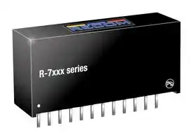
- Depth: 32.2mm
- Width: 9.1mm
- Height: 15mm
- Product Range: R-7 Series
- Output Power Max: 16.5W
- Output Current Max: 3A
- Output Voltage Max: 5.5V
- Output Voltage Min: 2.5V
- Input Voltage DC Max: 28V
- Input Voltage DC Min: 4.5V
- DC / DC Converter Type: SIP
- Power Supply Applications: ITE
- DC / DC Converter Output Type: Fixed, Adjustable
| Delivery and price | |
|---|---|
| Units per pack | 100 |
| Price | 22.14 € |
| Current stock | 25+ |
| Lead time | 30 days |
• Non-isolated Features • Synchronous rectification design • Adjustable output voltage **DC/DC Converter** • 2, 3, 4Amp adjustable positive step down Switching Integrated switching regulator • Over load protection Regulator • Continuous short circuit protection **R-7xxxP_D** e • Efficiency up to 97% ~~e~~ Po Description **2,3,4 Amp** The R-7xxx series is a high performance 2.5V to 17V, 2Amp to 4Amp, 12-Pin SIP (single in-line ~~PT~~ **SIP12** ©@ **3** package), integrated switching regulator (ISR). The synchronous - rectified design yields excellent efficiencies up to 97%. Short circuit protection reduces the short circuit input current to under 50mA. **Vertical & Horizontal** Selection Guide ~~|~~ Part Input Output Vout Output Efficiency Max. Capacitive **Single Output**[[(1)]][[(2)]] **r**

**==> picture [525 x 245] intentionally omitted <==**

**----- Start of picture text -----**<br>
|||||||||||
|---|---|---|---|---|---|---|---|---|---|
|Selection Guide|
|||
|Part|Input|Output|Vout|Output|Efficiency|Max. Capacitive|Single Output|
|Number|Voltage Range Voltage Adjust Range|[[(1)]]|Current|@ min Vin  @ max. Vin|Load|[[(2)]]|
|[VDC]|[VDC]|[VDC]|[A]|[%]|[%]|[µF]|
|R-723.3x|4.5 - 28|3.3|2.5 - 5.5|2|95|89|200/6800|
|R-725.0x|6.5 - 28|5.0|3.0 - 5.5|2|96|91|200/6800|
|R-726.5x|8.5 - 28|6.5|5.0 - 8.0|2|97|93|200/6800|
|R-729.0x|12 - 28|9.0|7.0 - 11|2|96|93|200/6800|
|R-7212x|15 - 28|12|10 - 14|2|97|95|200/6800|
|R-7215x|19 - 28|15|13 - 17|2|97|96|200/6800|
|R-733.3x|4.5 - 28|3.3|2.5 - 5.5|3|94|89|200/6800|
|R-735.0x|6.5 - 28|5.0|3.0 - 5.5|3|95|92|200/6800|
|R-736.5x|8.5 - 28|6.5|5.0 - 8.0|3|97|93|200/6800|
|R-739.0x|12 - 28|9.0|7.0 - 11|3|96|94|200/6800|
|R-7312x|15 - 28|12|10 - 14|3|97|96|200/6800|
|RoHS|2+|REACH|
|R-7315x|19 - 28|15|13 - 17|3|97|96|200/6800|compliant10 from 10|compliant|
|R-743.3x|4.5 - 28|3.3|2.5 - 5.5|4|93|88|200/6800|
|@|e|li|
|R-745.0x|6.5 - 28|5.0|3.0 - 5.5|4|95|91|200/6800|IEC/EN60950-1 certified|
|R-746.5x|8.5 - 28|6.5|5.0 - 7.5|4|96|93|200/6800|
|Notes:|
|T|T|

**----- End of picture text -----**<br>


Note1: Vin-Vout ≥ 1.5V~4.0V depending on Vout if adjust function is used Note2: Please refer to basic characteristics on page I-2

~~|~~ Model Numbering

R-7_ __ ~~|~~ x Output Current (A) Pinning[(3)] ~~=~~ nom. Output Voltage

Notes:

Note3:  x can be „P“ = vertical through hole

x can be „D“ = bent pins for horizontal through hole mounting

## Ordering Examples:

R-723.3P Iout= 2A R-7312D Iout= 3A

nom. Vout= 3.3VDC P= vertical through hole nom. Vout= 12VDC D= horizontal through hole

REV.:  7/2020

I-1

**www.recom-power.com**

## **R-7xxxP_D**

## **DC/DC Converter**

## **Series**

Specifications (refer to standard application circuit, Ta= 25°C)

|BASIC CHARACTERISTICS|BASIC CHARACTERISTICS|||||
|---|---|---|---|---|---|
|Parameter||Condition|Min.|Typ.|Max.|
|Quiescent Current||min. Vin to max.|||30mA|
|Internal Power Dissipation||ta<60°C|||1.4W|
|Output Current Limit||R-72xxx<br>R-73xxx<br>R-74xxx||2.5A<br>3.75A<br>5.0A|3.0A<br>4.25A<br>5.5A|
|Minimum Load|||10%|||
|ON/OFF CTRL(4)||DC-DC ON<br>DC-DC OFF|Open or high, 4.5V min. / 28V max.<br>Low(Power OFF)0.8V max.|||
|Input Current of CTRL Pin||DC-DC OFF|||100µA|
|Internal Operating Frequency|||270kHz|300kHz|330kHz|
|Output Ripple and Noise||||40mVp-p|70mVp-p|
|Maximum Capacitive Load||normal start-uptime, no external diodes|||200µF|
|||<1 second start-uptime + diodeprotection circuit|||6800µF|
|continued on nextpage<br>How to calculate the max. output current<br>Calculation 1:<br>Calculation 2:<br>Calculation 3:<br>Notes:<br>Note4: ON/OFF pin driven by TTL (logic gate), open-collector bipolar transistor or open-drain MOSFET<br>0<br>0.5<br>0<br>20<br>40<br>60<br>80<br>85<br>100<br>Ambient Temperature [°C]<br>Internal Power Dissipation [W]<br>1.4<br>1<br>Vin = 28V<br>Vout = 5V<br>Effmax Vin= 91%<br>PD= 1.4W<br>TAmbient= 60°C<br>Vin = 28V<br>Vout = 5V<br>Effmax Vin= 91%<br>PD= 1.0W<br>TAmbient= 85°C<br>Vin = 12V<br>Effmax Vin= 94%<br>PD= 1.0W<br>TAmbient= 85°C<br>Example: R-745.0P<br>Iout=<br>1.4W<br>= 3.11A<br>5V x (1-0.91 )<br>Iout=<br>1W<br>= 2.222A<br>5V x (1-0.91 )<br>Iout=<br>1W<br>= 3.33A<br>5V x (1-0.94 )<br>Iout=<br>PD<br>Vout x (1-Effmax Vin)<br>PD=<br>Iout x Vout x (1-Effmax Vin)<br>The internal power dissipation (PD) follows the equation:|Notes:|||||


REV.:  7/2020

I-2

**www.recom-power.com**

## **R-7xxxP_D**

## **DC/DC Converter**

## **Series**

Specifications (refer to standard application circuit, Ta= 25°C)

Efficiency vs. Load

**==> picture [203 x 190] intentionally omitted <==**

**----- Start of picture text -----**<br>
R-72xx / R-73xx / R-74xx<br>max. Vin<br>100<br>90<br>80<br>70<br>60<br>15Vout<br>50 5Vout<br>3.3Vout<br>40<br>0 1 2 3 4<br>Output Current [A]<br>Efficiency [%]<br>**----- End of picture text -----**<br>


Efficiency vs. Input Voltage

**==> picture [205 x 185] intentionally omitted <==**

**----- Start of picture text -----**<br>
R-72xx / R-73xx<br>100<br>90<br>80<br>70<br>60<br>50<br>40<br>30<br>15Vout<br>20 6.5Vout<br>5Vout<br>10<br>3.3Vout<br>0<br>0 5 10 15 20 25 28<br>Input Voltage [VDC]<br>Efficiency [%]<br>**----- End of picture text -----**<br>


**==> picture [207 x 423] intentionally omitted <==**

**----- Start of picture text -----**<br>
R-72xx / R-73xx / R-74xx<br>min. Vin<br>100<br>95<br>90<br>85<br>80<br>6.5Vout<br>75<br>5Vout<br>3.3Vout<br>70<br>0 1 2 3 4<br>Output Current [A]<br>R-74xx<br>100<br>90<br>80<br>70<br>60<br>50<br>40<br>30<br>20 6.5Vout<br>5Vout<br>10 3.3Vout<br>0<br>0 5 10 15 20 25 28<br>Input Voltage [VDC]<br>Efficiency [%]<br>Efficiency [%]<br>**----- End of picture text -----**<br>


Ripple vs. Input Voltage

**==> picture [486 x 187] intentionally omitted <==**

**----- Start of picture text -----**<br>
R-72xx / R-73xx R-74xx<br>50 100<br>45 90<br>40 80<br>35 70<br>30 60<br>25 50<br>20 40<br>15 30<br>10 15Vout 6.5Vout 20 6.5Vout<br>12Vout 5Vout 5Vout<br>5 9Vout 3.3Vout 10 3.3Vout<br>0 0<br>0 5 10 15 20 25 28 0 5 10 15 20 25 28<br>Input Voltage [VDC] Input Voltage [VDC]<br>Ripple (mV)<br>Ripple (mV)<br>**----- End of picture text -----**<br>


REV.:  7/2020

I-3

**www.recom-power.com**

## **R-7xxxP_D**

## **DC/DC Converter**

## **Series**

Specifications (refer to standard application circuit, Ta= 25°C)

|2ADC<br>R-723.3P/D<br>R-725.0P/D<br>R-726.5P/D<br>R-729.0P/D<br>R-7212P/D<br>R-7215P/D<br>3ADC<br>R-733.3P/D<br>R-735.0P/D<br>R-736.5P/D<br>R-739.0P/D<br>R-7312P/D<br>R-7315P/D<br>4ADC<br>R-743.3P/D<br>R-745.0P/D<br>R-746.5P/D|2ADC<br>R-723.3P/D<br>R-725.0P/D<br>R-726.5P/D<br>R-729.0P/D<br>R-7212P/D<br>R-7215P/D<br>3ADC<br>R-733.3P/D<br>R-735.0P/D<br>R-736.5P/D<br>R-739.0P/D<br>R-7312P/D<br>R-7315P/D<br>4ADC<br>R-743.3P/D<br>R-745.0P/D<br>R-746.5P/D|2ADC<br>R-723.3P/D<br>R-725.0P/D<br>R-726.5P/D<br>R-729.0P/D<br>R-7212P/D<br>R-7215P/D<br>3ADC<br>R-733.3P/D<br>R-735.0P/D<br>R-736.5P/D<br>R-739.0P/D<br>R-7312P/D<br>R-7315P/D<br>4ADC<br>R-743.3P/D<br>R-745.0P/D<br>R-746.5P/D|2ADC<br>R-723.3P/D<br>R-725.0P/D<br>R-726.5P/D<br>R-729.0P/D<br>R-7212P/D<br>R-7215P/D<br>3ADC<br>R-733.3P/D<br>R-735.0P/D<br>R-736.5P/D<br>R-739.0P/D<br>R-7312P/D<br>R-7315P/D<br>4ADC<br>R-743.3P/D<br>R-745.0P/D<br>R-746.5P/D|2ADC<br>R-723.3P/D<br>R-725.0P/D<br>R-726.5P/D<br>R-729.0P/D<br>R-7212P/D<br>R-7215P/D<br>3ADC<br>R-733.3P/D<br>R-735.0P/D<br>R-736.5P/D<br>R-739.0P/D<br>R-7312P/D<br>R-7315P/D<br>4ADC<br>R-743.3P/D<br>R-745.0P/D<br>R-746.5P/D|2ADC<br>R-723.3P/D<br>R-725.0P/D<br>R-726.5P/D<br>R-729.0P/D<br>R-7212P/D<br>R-7215P/D<br>3ADC<br>R-733.3P/D<br>R-735.0P/D<br>R-736.5P/D<br>R-739.0P/D<br>R-7312P/D<br>R-7315P/D<br>4ADC<br>R-743.3P/D<br>R-745.0P/D<br>R-746.5P/D|2ADC<br>R-723.3P/D<br>R-725.0P/D<br>R-726.5P/D<br>R-729.0P/D<br>R-7212P/D<br>R-7215P/D<br>3ADC<br>R-733.3P/D<br>R-735.0P/D<br>R-736.5P/D<br>R-739.0P/D<br>R-7312P/D<br>R-7315P/D<br>4ADC<br>R-743.3P/D<br>R-745.0P/D<br>R-746.5P/D|2ADC<br>R-723.3P/D<br>R-725.0P/D<br>R-726.5P/D<br>R-729.0P/D<br>R-7212P/D<br>R-7215P/D<br>3ADC<br>R-733.3P/D<br>R-735.0P/D<br>R-736.5P/D<br>R-739.0P/D<br>R-7312P/D<br>R-7315P/D<br>4ADC<br>R-743.3P/D<br>R-745.0P/D<br>R-746.5P/D|2ADC<br>R-723.3P/D<br>R-725.0P/D<br>R-726.5P/D<br>R-729.0P/D<br>R-7212P/D<br>R-7215P/D<br>3ADC<br>R-733.3P/D<br>R-735.0P/D<br>R-736.5P/D<br>R-739.0P/D<br>R-7312P/D<br>R-7315P/D<br>4ADC<br>R-743.3P/D<br>R-745.0P/D<br>R-746.5P/D|2ADC<br>R-723.3P/D<br>R-725.0P/D<br>R-726.5P/D<br>R-729.0P/D<br>R-7212P/D<br>R-7215P/D<br>3ADC<br>R-733.3P/D<br>R-735.0P/D<br>R-736.5P/D<br>R-739.0P/D<br>R-7312P/D<br>R-7315P/D<br>4ADC<br>R-743.3P/D<br>R-745.0P/D<br>R-746.5P/D|2ADC<br>R-723.3P/D<br>R-725.0P/D<br>R-726.5P/D<br>R-729.0P/D<br>R-7212P/D<br>R-7215P/D<br>3ADC<br>R-733.3P/D<br>R-735.0P/D<br>R-736.5P/D<br>R-739.0P/D<br>R-7312P/D<br>R-7315P/D<br>4ADC<br>R-743.3P/D<br>R-745.0P/D<br>R-746.5P/D|2ADC<br>R-723.3P/D<br>R-725.0P/D<br>R-726.5P/D<br>R-729.0P/D<br>R-7212P/D<br>R-7215P/D<br>3ADC<br>R-733.3P/D<br>R-735.0P/D<br>R-736.5P/D<br>R-739.0P/D<br>R-7312P/D<br>R-7315P/D<br>4ADC<br>R-743.3P/D<br>R-745.0P/D<br>R-746.5P/D|2ADC<br>R-723.3P/D<br>R-725.0P/D<br>R-726.5P/D<br>R-729.0P/D<br>R-7212P/D<br>R-7215P/D<br>3ADC<br>R-733.3P/D<br>R-735.0P/D<br>R-736.5P/D<br>R-739.0P/D<br>R-7312P/D<br>R-7315P/D<br>4ADC<br>R-743.3P/D<br>R-745.0P/D<br>R-746.5P/D|
|---|---|---|---|---|---|---|---|---|---|---|---|---|
|Vout nom.<br>3.3VDC<br>5.0VDC<br>6.5VDC<br>9.0VDC<br>12VDC<br>15VDC|||||||||||||
|Vout adj.|Rdown|Rup|Rdown|Rup|Rdown|Rup|Rdown|Rup|Rdown|Rup|Rdown|Rup|
|2.5|8.5kΩ||||||||||||
|3.0|33kΩ||470Ω||||||||||
|3.2|110kΩ||1.6kΩ||||||||||
|3.3|||2.2kΩ||||||||||
|3.4||36kΩ|3.0kΩ||||||||||
|3.6||11kΩ|4.7kΩ||||||||||
|3.9||4.7kΩ|8.5kΩ||||||||||
|4.5||1.6kΩ|30kΩ||||||||||
|4.9||820Ω|220kΩ||||||||||
|5.0||680Ω|||11kΩ||||||||
|5.1||560Ω||28kΩ|12kΩ||||||||
|5.5||190Ω||2.6kΩ|20kΩ||||||||
|6.0|||||47kΩ||||||||
|6.5|||||||||||||
|7.0||||||4.5kΩ|13kΩ||||||
|7.5||||||2.2kΩ|||||||
|8.0|||||||31kΩ||||||
|9.0|||||||||||||
|10||||||||2.2kΩ|20kΩ||||
|11||||||||390Ω|47kΩ||||
|12|||||||||||||
|13||||||||||2.4kΩ|36kΩ||
|14||||||||||390Ω|76kΩ||
|15|||||||||||||
|16||||||||||||2.6kΩ|
|17||||||||||||860Ω|


|REGULATIONS||||
|---|---|---|---|
|Parameter||Condition|Value|
|Output Accuracy||full load|±1.0% typ. / ±2.0% max.|
|Line Regulation||low line to high line, full load|± 0.5% typ. / ±1.0% max.|
|Load Regulation(5)||10% to 100%, full load|± 0.5% typ. / ±1.0% max.|
|Transient Response(6)||50% load step change<br>Vout Over / Undershoot|100µs typ. / 200µs max.<br>100mV max.|
||Notes:<br>Note5: Operation below 10% load will not harm the converter, but specifcations may not be met<br>Note6: Requires a 100µF electrolytic or tantalum output capacitor for proper operation in all applications<br>(the capacitor has to be placed as close as possible to the output pins)|||


REV.:  7/2020

I-4

**www.recom-power.com**

## **R-7xxxP_D**

## **DC/DC Converter**

## **Series**

Specifications (refer to standard application circuit, Ta= 25°C)

**==> picture [526 x 234] intentionally omitted <==**

**----- Start of picture text -----**<br>
PROTECTIONS<br>Parameter  Condition Value<br>Short Circuit Protection (SCP) continuous, automatic recovery<br>Short Circuit Input Current 50mA typ. / 100mA max.<br>Optional Diode Protection Circuit<br>Optional Protection 1: Optional Protection :<br>Add a blocking diode to Vout if current  D1<br>can flow backwards into the output, as<br>this can damage the converter when it is powered down. Protection diodes are required for high capacitive loads. +Vin +Vin R-5/6/7xxxGND +Vout +Vout +Vin +Vin R-5/6/7xxxGND Vadj +Vout D1 +Vout<br>The diode can either be fitted across  Rdown<br>the device, if the source is low imped-<br>ance or fitted in series with the output  GND GND GND GND<br>(recommended). Rdown: Trim output voltage up to 1 diode drop<br>**----- End of picture text -----**<br>


|ENVIRONMENTAL|ENVIRONMENTAL|ENVIRONMENTAL|ENVIRONMENTAL|
|---|---|---|---|
|Parameter|Condition||Value|
|OperatingTemperature Range|without derating@ natural convection 0.1m/s||-40°C to +85°C|
|Maximum Case Temperature|||+110°C|
|Thermal Impedance|@ natural convection 0.1m/s||25°C/W|
|OperatingHumidity|non-condensing||95% RH max.|
|OperatingAltitude|||2000m|
|Pollution Degree|||PD2|
|MTBF|according to MIL-HDBK 217F, G.B.|+25°C<br>+85°C|749 x 103hours<br>150 x 103hours|


|SAFETY AND CERTIFICATIONS|SAFETY AND CERTIFICATIONS|SAFETY AND CERTIFICATIONS|
|---|---|---|
|Certifcate Type(Safety)|Report / File Number|Standard|
|Information Technology Equipment, General Requirements for Safety|1605077-12|IEC60950-1:2005, 2nd Edition + AM2:2013<br>EN60950-1:2006 + AM2:2013|
|EAC|RU-AT.49.09571|TP TC 004/2011|
|RoHS 2+||RoHS-2011/65/EU + AM-2015/863|
|continued on nextpage|||


REV.:  7/2020

I-5

**www.recom-power.com**

## **R-7xxxP_D**

## **DC/DC Converter**

## **Series**

Specifications (refer to standard application circuit, Ta= 25°C)

EMC Filtering Suggestions according to EN55032

|C1<br>C2<br>GND<br>L2<br>L1<br>+Vin<br>Component List<br>EN55022<br>C1<br>Class A<br>N/A<br>Class B<br>10µF|L1|L1|C2<br>L2|C2<br>L2|C4<br>R-746.5<br>C3<br>GND<br>+Vo<br>+Vin|C4<br>R-746.5<br>C3<br>GND<br>+Vo<br>+Vin|C4<br>R-746.5<br>C3<br>GND<br>+Vo<br>+Vin|C4<br>R-746.5<br>C3<br>GND<br>+Vo<br>+Vin|GND<br>ut<br>+Vout|GND<br>ut<br>+Vout|GND<br>ut<br>+Vout|
|---|---|---|---|---|---|---|---|---|---|---|---|
||||||||R-746.5<br>GND<br>+Vo<br>+Vin|||||
||C1||C2||C3|||||||
|||||||||||||
|||||||||||||
|||||||||||||
|||EN55022||C1|C2|C3||C4||L1|L2|
|||Class A||N/A|33µF|||N/A||N/A|0.45mH CMC|
|||Class B||10µF|33µF<br>|||1nF/2kV||2mH|0.45mH CMC|


**==> picture [526 x 466] intentionally omitted <==**

**----- Start of picture text -----**<br>
DIMENSION AND PHYSICAL CHARACTERISTICS<br>Parameter Type Value<br>case non-conducive black plastic, (UL94 V-0)<br>Material<br>potting epoxy, (UL94 V-0)<br>Dimension (LxWxH) 32.2 x 9.1 x 15.0mm<br>Weight 9g typ.<br>Dimension Drawing (mm)<br>32.2<br>R-7xxxD<br>embossed logo<br>32.2 9.1<br>R-7xxxP Marking<br>2.1 0.70 [+0.10/-0.05] 0.25 [±0.05]<br>11 x 2.54 = 27.94 Recommended Footprint Details 2.1 0.70 [+0.10/-0.05] 0.25 [±0.05]<br>Recommended Footprint Details<br>1 2 3 4 5 6 7 8 9 10 11 12<br>Top View Bottom View 1 2 3 4 5 6 7 8 9 10 11 12<br>Bottom View<br>1 2 3 4 5 6 7 8 9 10 11 12 Top View<br>1 2 3 4 5 6 7 8 9 10 11 12 11 x 2.54 = 27.94<br>2.54<br>2.54<br>Pin Connections<br> Pin #  Single  Description<br>1  ON/OFF  Input pin: Active low (less than 0.8V) to disable the device<br>  2,3,4  Vin  Power Input<br> 5, 6, 7, 8  GND  Input and Output ground (common)<br> 9, 10, 11  Vout  Power output<br>12  Vadj  with external resistors R1, R2 to selected output voltage<br>Tolerance:   xx.x= ±0.5mm<br>xx.xx= ±0.25mm<br>15.0<br>15.0<br>9.1<br>4.10<br>2.54<br>17.0<br>2.54<br>0.8<br>**----- End of picture text -----**<br>


REV.:  7/2020

I-6

**www.recom-power.com**

## **R-7xxxP_D**

## **DC/DC Converter**

## **Series**

Specifications (refer to standard application circuit, Ta= 25°C)

**==> picture [526 x 195] intentionally omitted <==**

**----- Start of picture text -----**<br>
INSTALLATION AND APPLICATION<br>Standard Application Circuit<br>+V +Vin +Vout +V<br>in out<br>R-7xxxP_D<br>OFF 1µF C1<br>(Optional) ON/OFF GND V Rdown<br>ON adj C2<br>100µF<br>VCTRL Q1 ESR= 150m Ω  max.<br>(Required)<br>R<br>up<br>Com Com<br>Add blocking diode to Vout if current can flow backwards into the output, as this can damage the converter.<br>(Please refer to “Optional Diode Protection Circuit” on Page I-5)<br>**----- End of picture text -----**<br>


|PACKAGING INFORMATION|PACKAGING INFORMATION|PACKAGING INFORMATION|
|---|---|---|
|Parameter|Type|Value|
|Packaging Dimensions (LxWxH)|R-7xxxD<br>R-7xxxP|520.0 x 20.0 x 19.0mm<br>530.0 x 23.0 x 19.0mm|
|PackagingQuantity|tube|15pcs|
|Storage Temperature Range||-40°C to +125°C|


The product information and specifications may be subject to changes even without prior written notice.The product has been designed for various applications; its suitability lies in the responsibility of each customer. The products are not authorized for use in safety-critical applications without RECOM’s explicit written consent. A safety-critical application is an application where a failure may reasonably be expected to endanger or cause loss of life, inflict bodily harm or damage property. The applicant shall indemnify and hold harmless RECOM, its affiliated companies and its representatives against any damage claims in connection with the unauthorized use of RECOM products in such safety-critical applications.

REV.:  7/2020

I-7

**www.recom-power.com**
Updated at April 28, 2026
RECOM Power is a globally recognized manufacturer specializing in standard and customized power conversion solutions. Headquartered in Austria with state-of-the-art research and development facilities, the company has built a strong reputation for innovation and reliability. Operating from ISO 9001 and IATF 16949 certified manufacturing sites, RECOM delivers premium power supplies engineered for demanding applications across IoT, Industry 4.0, medical technology, and transportation. The core of our RECOM Power portfolio is dedicated to advanced power and line protection, featuring an extensive selection of high-performance AC/DC converters. These modules are designed to provide efficient, stable power distribution for a wide array of industrial and commercial electronics. In addition to general-purpose power supplies, we offer a robust range of AC/DC LED power supplies specifically optimized to meet the stringent efficiency and lifespan requirements of modern lighting systems. To support comprehensive power architecture design, our selection also includes highly efficient DC/DC converters ideal for precise voltage regulation in complex circuits. Furthermore, we provide specialized passive components such as RECOM power inductors, ensuring engineers have access to the critical, high-quality components required to develop resilient and optimized power delivery systems.
About Novapart
Novapart is a B2B electronic component broker specialising in stock shortages and cost reduction. We source hard-to-find parts and identify compliant alternatives across a catalogue of 410,000+ components from 500+ manufacturers.
Learn more →Stock Shortage Specialist
When a component is unavailable, discontinued or has an unacceptable lead time, we tap into our network of vetted European and Asian distributors to source what you need — without compromising on quality or traceability.
Request a quote →Compliant Alternatives
We identify pin-to-pin, electrically equivalent substitutes that meet the same certifications (RoHS, AEC-Q100, REACH) as your original specification — validated against datasheets, not just part numbers. Often at a lower cost.
BOM Analysis service →