


Q6016LH6TP
Triac, 600 V, 16 A, TO-220AB, 1.3 V, 167 A, 70 mA
- Manufacturer: LITTELFUSE
- Product type:
- Peak Repetitive Off-State Voltage, Vdrm:600V; On State RMS Current IT(rms):16A; Triac Case Style:TO-220AB; Gate Trigger Current Max (QI), Igt:80mA; Gate Trigger Voltage Max Vgt:1.3V; Peak Gate
- MSL: MSL 1 - Unlimited
- SVHC: To Be Advised
- No. of Pins: 3Pins
- Product Range: Qxx16xHx
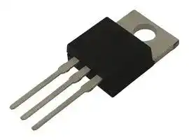
- Triac Case Style: TO-220AB
- Thyristor Mounting: Through Hole
- Holding Current Max: 70mA
- On State RMS Current: 16A
- Peak On State Voltage: 1.6V
- Gate Trigger Voltage Max: 1.3V
- Operating Temperature Max: 125°C
- Peak Non Repetitive Surge Current: 167A
- Peak Repetitive Off State Voltage: 600V
| Delivery and price | |
|---|---|
| Units per pack | 1000 |
| Price | 1.18 € |
| Current stock | 1000+ |
| Lead time | 30 days |
**Thyristors** 15 Amp Standard & 16 Amp Alternistor (High Commutation) Triacs

~~**RoHS** A~~

## ~~Qxx15xx & Qxx16xHx Series~~

**Description** This 15 Amp and 16 Amp bi-directional solid state switch ~~Lo~~ series is designed for AC switching and phase control applications such as motor speed, temperature modulation controls, lighting controls, and static switching relays.

Standard type devices normally operate in Quadrants I & III triggered from AC line.

Standard alternistor triac components operate with in-phase signals in Quadrants I or III and ONLY unipolar negative gate pulses  for Quadrant II or III. The alternistor triac will not operate in Quadrant IV. These are used in circuit applications requiring a high dv/dt capability.

**==> picture [505 x 171] intentionally omitted <==**

**----- Start of picture text -----**<br>
Agency Approval Features & Benefits<br>ee eee<br>a Agency ee Agency File Number •   RoHS-compliant  contact bounce that<br>create voltage transients<br>E71639* •   Glass – passivated<br>a junctions •   No contacts to wear<br>* - L Package only<br>out from reaction of<br>•   Voltage capability up to<br>switching events<br>1000 V<br>•   Restricted (or limited) RFI<br>Main Features •   Surge capability up to<br>Po generation, depending<br>200 A<br>on activation point in sine<br>Symbol Value Unit •   The L-package has  wave<br>IT(RMS) 15 or 16 A an isolation rating of  •   Requires only a small<br>VDRM/VRRM 400, 600, 800 or 1000 V 2500VRMSRMSRMS gate activation pulse in<br>IGT (Q1) 10, 20, 35, 50 or 80 mA •   Solid-state switching  each half-cycle<br>**----- End of picture text -----**<br>


- Restricted (or limited) RFI

- •   Surge capability up to generation, depending

- 200 A on activation point in sine

- •   The L-package has wave an isolation rating of •   Requires only a small

- 2500VRMSRMSRMS

- Requires only a small

- 2500VRMSRMSRMS gate activation pulse in

- •   Solid-state switching each half-cycle eliminates arcing or

**==> picture [243 x 19] intentionally omitted <==**

**----- Start of picture text -----**<br>
Schematic Symbol<br>ee,<br>**----- End of picture text -----**<br>


## **Applications**

Excellent for AC switching and phase control applications such as heating, lighting, and motor speed controls.

**==> picture [150 x 46] intentionally omitted <==**

**----- Start of picture text -----**<br>
MT2 MT1<br>G<br>**----- End of picture text -----**<br>


**==> picture [243 x 69] intentionally omitted <==**

**----- Start of picture text -----**<br>
Additional Information<br>Lo<br>a<br>Datasheet Resources Samples<br>**----- End of picture text -----**<br>


Typical applications are AC solid-state switches, light dimmers, power tools, lawn care equipment, home/brown goods and white goods appliances.

Alternistor Triacs (no snubber required) are used in applications with extremely inductive loads requiring highest commutation performance.

Internally constructed isolated packages are offered for ease of heat sinking with highest isolation voltage.

©2019 Littelfuse, Inc Specifications are subject to change without notice. Revised: BO.12/11/20

**Thyristors** 15 Amp Standard & 16 Amp Alternistor (High Commutation) Triacs

## **Absolute Maximum Ratings — Standard Triac**

**==> picture [506 x 146] intentionally omitted <==**

**----- Start of picture text -----**<br>
Symbol Parameter Value Unit<br>Qxx15Ly TC = 80°C<br>IT(RMS) RMS on-state current  (full sine wave) Qxx15NyQxx15Ry  TC = 90°C 15 A<br>ITSM Non repetitive surge peak on-state current  (full cycle, TJ initial = 25°C) f = 60 Hzf = 50 Hz t = 16.7 mst = 20 ms 200167 A<br>I [2] t I [2] t Value for fusing - tp = 8.3 ms 166 A [2] s<br>di/dt Critical rate of rise of on-state current f = 120 Hz TJ = 125°C 100 A/μs<br>IGTM Peak gate trigger current tp=20μs TJ = 125°C 4 A<br>PG(AV) Average gate power dissipation TJ = 125°C 0.5 W<br>Tstg Storage temperature range - -40 to 150 ºC<br>TJ Operating junction temperature range - -40 to 125 ºC<br>**----- End of picture text -----**<br>


**Note:** xx = voltage/10, y = sensitivity

## **Absolute Maximum Ratings — Alternistor Triac (3 Quadrants)**

**==> picture [506 x 147] intentionally omitted <==**

**----- Start of picture text -----**<br>
Symbol Parameter Value Unit<br>Qxx16LHy TC = 80°C<br>IT(RMS) RMS on-state current (full sine wave) Qxx16NHyQxx16RHy  TC = 90°C 16 A<br>ITSM Non repetitive surge peak on-state current  (full cycle, TJ initial = 25°C) f = 50 Hzf = 60 Hz t = 16.7 mst = 20 ms 200167 A<br>I [2] t I [2] t Value for fusing tp = 8.3 ms 166 A [2] s<br>di/dt Critical rate of rise of on-state current f = 120 Hz TJ = 125°C 100 A/μs<br>IGTM Peak gate trigger current tp=20μs TJ = 125°C 4 A<br>PG(AV) Average gate power dissipation TJ = 125°C 0.5 W<br>Tstg Storage temperature range -40 to 150 ºC<br>TJ Operating junction temperature range -40 to 125 ºC<br>**----- End of picture text -----**<br>


**Note:** xx = voltage/10, y = sensitivity

## **Electrical Characteristics (TJ = 25°C, unless otherwise specified) — Standard Triac**

**==> picture [506 x 142] intentionally omitted <==**

**----- Start of picture text -----**<br>
Symbol Test Conditions Quadrant  Value Unit<br>IGT VD = 12V  RL = 60 Ω I – II – III MAX. 50 mA<br>VGT VD = 12V  RL = 60 Ω I – II – III MAX. 2.0 V<br>VGD VD = VDRM  RL = 3.3 kΩ  TJ = 125°C I – II – III MIN. 0.2 V<br>IH IT = 100mA MAX. 70 mA<br>400V 275<br>dv/dt VD = VDRM  Gate Open  TJ = 125°C 600V MIN. 225 V/μs<br>800V 200<br>VD = VDRM  Gate Open  TJ = 100°C 1000V 200<br>(dv/dt)c (di/dt)c = 8.1 A/ms  TJ = 125°C MIN. 4 V/μs<br>tgt IG = 2 x IGT PW = 15μs  IT = 22.6 A(pk) TYP. 4 μs<br>**----- End of picture text -----**<br>


©2019 Littelfuse, Inc Specifications are subject to change without notice. Revised: BO.12/11/20

15 Amp Standard & 16 Amp Alternistor (High Commutation) Triacs

## **Thyristors**

## **Electrical Characteristics (TJ = 25°C, unless otherwise specified) — Alternistor Triac (3 Quadrants)**

**==> picture [506 x 395] intentionally omitted <==**

**----- Start of picture text -----**<br>
Symbol Test Conditions Quadrant  Qxx16xH2 Qxx16xH3 Qxx16xH4 Qxx16xH6 Unit<br>IGT VD = 12V  RL = 60 Ω I – II – III MAX. 10 20 35 80 mA<br>VGT VD = 12V  RL = 60 Ω I – II – III MAX. 1.3 V<br>VGD VD = VDRM  RL = 3.3 kΩ  TJ = 125°C I – II – III MIN. 0.2 V<br>IH IT = 100mA MAX. 15 35 50 70 mA<br>400V 200 350 475 925<br>dv/dt VD = VDRM  Gate Open  TJ = 125°C 600V MIN. 150 250 400 850 V/μs<br>800V 100 200 350 475<br>VD = VDRM  Gate Open  TJ = 100°C 1000V 100 200 300 350<br>(dv/dt)c (di/dt)c = 8.6 A/ms  TJ = 125°C MIN. 2 20 25 30 V/μs<br>tgt IG = 2 x IGT  PW = 15μs  IT = 22.6 A(pk) TYP. 3 3 3 5 μs<br>Static Characteristics<br>Symbol Test Conditions Value Unit<br>VTM 16A Device I15A Device ITT = 22.6A t = 21.2A tpp = 380μs = 380μs MAX 1.60 V<br>TJ = 25°C 400-1000V 5 μA<br>IIDRMRRM VD = VDRM / VRRM TJ = 125°C 400-800V MAX 2 mA<br>TJ = 100°C 1000V 3<br>Thermal Resistances<br>Symbol Parameter Value Unit<br>Qxx15Ry<br>Qxx15Ny  1.7<br>Qxx16RHy<br>R Ɵ (J-C) Junction to case (AC) Qxx16NHy °C/W<br>Qxx15Ly  2.1<br>Qxx16LHy<br>Qxx15Ry  45<br>Qxx16RHy<br>R Ɵ (J-A) Junction to ambient Qxx15Ly  50 °C/W<br>Qxx16LHy<br>**----- End of picture text -----**<br>


**Note:** xx = voltage/10; y = sensitivity

## **Figure 1:  Definition of Quadrants**

**==> picture [243 x 172] intentionally omitted <==**

**----- Start of picture text -----**<br>
ALL POLARITIES ARE REFERENCED TO MT1<br>MT2 POSITIVE<br>MT2 (Positive Half Cycle)+ MT2<br>(-) I G T (+) I G T<br>GATE GATE<br>MT1 MT1<br>REF REF<br>I G T - QIIIQII QIQIV  +  I G T<br>MT2 MT2<br>(-) I G T (+) I G T<br>GATE GATE<br>MT1 MT1<br>-<br>REF MT2 NEGATIVE REF<br>(Negative Half Cycle)<br>**----- End of picture text -----**<br>


**==> picture [243 x 204] intentionally omitted <==**

**----- Start of picture text -----**<br>
Figure 2:  Normalized DC Gate Trigger Current for All<br>Quadrants vs. Junction Temperature<br>4.0<br>3.0<br>2.0<br>1.0<br>0.0<br>-65             -40 -15 10 35 60 85 100 +125<br>Junction Temperature (TJ) - ºC<br>= 25ºC)(TJ<br>GT<br> / I<br>GT<br>Ratio of  I<br>**----- End of picture text -----**<br>


**Note:** Alternistors will not operate in QIV

©2019 Littelfuse, Inc Specifications are subject to change without notice.

Revised: BO.12/11/20

**Thyristors** 15 Amp Standard & 16 Amp Alternistor (High Commutation) Triacs

**==> picture [243 x 461] intentionally omitted <==**

**----- Start of picture text -----**<br>
Figure 3:  Normalized DC Holding Current<br>vs. Junction Temperature<br>4.0<br>3.0<br>2.0<br>1.0<br>0.0<br>-65             -40             -15              10              35               60              85              100 +125<br>Junction Temperature (TJ) - ºC<br>Figure 5:  Power Dissipation (Typical)<br>vs. RMS On-State Current<br>18<br>16<br>14<br>12<br>10<br>8<br>6<br>4<br>2<br>0<br>0              2              4             6              8             10            12            14           16            18<br>RMS On-State Current [IT(RMS)] - AMPS<br>Figure 7:  Maximum Allowable Case Temperature<br>vs. On-State Current (16A devices)<br>= 25ºC)(TJ<br>IH<br> / I<br>IH<br>Ratio of  I<br>] - Watts<br>D(AV)<br>[P<br>Average On-State Power Dissipation<br>**----- End of picture text -----**<br>


**==> picture [243 x 175] intentionally omitted <==**

**----- Start of picture text -----**<br>
130<br>120<br>Qxx16RHy<br>Qxx16NHy<br>110<br>100<br>Qxx16LHy<br>90<br>80 CURRENT WAVEFORM:  Sinusoidal<br>LOAD:  Resistive or Inductive<br>CONDUCTION ANGLE:  360<br>70 CASE TEMPERATURE:  Measured as shown<br>                                          on dimensional drawing<br>60<br>0                                5                              10                              15                             20<br>RMS On-State Current [IT(RMS)] - AMPS<br>(T) - ºCC<br>Max Allowable Case Temperature<br>**----- End of picture text -----**<br>


**==> picture [243 x 208] intentionally omitted <==**

**----- Start of picture text -----**<br>
Figure 4:  Normalized DC Gate Trigger Voltage for<br>All Quadrants vs. Junction Temperature<br>2.0<br>1.5<br>1.0<br>0.5<br>0.0<br>-65             -40             -15              10              35              60              85            100 +125<br>Junction Temperature (TJ) - ºC<br> = 25ºC)(TJ<br>GT<br> / V<br>GT<br>Ratio of  V<br>**----- End of picture text -----**<br>


**==> picture [243 x 28] intentionally omitted <==**

**----- Start of picture text -----**<br>
Figure 6:  Maximum Allowable Case Temperature<br>vs. On-State Current (15A devices)<br>**----- End of picture text -----**<br>


**==> picture [243 x 392] intentionally omitted <==**

**----- Start of picture text -----**<br>
130<br>120<br>110<br>Qxx15R5<br>100 Qxx15N5<br>90<br>Qxx15L5<br>80 CURRENT WAVEFORM:  Sinusoidal<br>LOAD:  Resistive or InductiveCONDUCTION ANGLE:  360o<br>70 CASE TEMPERATURE:  Measured as shown<br>                                          on dimensional drawing<br>60<br>0                                      5                                    10                                    15<br>RMS On-State Current [IT(RMS)] - AMPS<br>Figure 8:  Maximum Allowable Ambient Temperature<br>vs. On-State Current<br>120<br>110<br>100 Qxx15Ry<br>Qxx15L<br>90 Qxx16RHQxx16LHyy<br>80<br>70<br>60<br>50 CURRENT WAVEFORM:  Sinusoidal<br>LOAD:  Resistive or Inductive<br>40 CONDUCTION ANGLE:  360<br>CASE TEMPERATURE:  Measured as shown<br>30                                           on dimensional drawing<br>20<br>0.0         0.2         0.4          0.6         0.8         1.0          1.2          1.4         1.6          1.8          2.0<br>RMS On-State Current [IT(RMS)] - AMPS<br>) - ºCMax Allowable Case Temperature (TC<br>(T) - ºCA<br>Max Allowable Ambiant Temperature<br>**----- End of picture text -----**<br>


©2019 Littelfuse, Inc Specifications are subject to change without notice.

Revised: BO.12/11/20

**Thyristors** 15 Amp Standard & 16 Amp Alternistor (High Commutation) Triacs

**==> picture [504 x 394] intentionally omitted <==**

**----- Start of picture text -----**<br>
Figure 9:  On-State Current  vs. On-State Voltage (Typical)<br>70<br>TJ = 25ºC<br>60<br>50<br>40<br>30<br>20<br>10<br>0<br>0.6                0.8                1.0               1.2                1.4                1.6                1.8                2.0<br>Positive or Negative Instantaneous On-State Voltage (VT) - Volts<br>Figure 10:  Surge Peak On-State Current vs. Number of Cycles<br>1000<br>Supply Frequency:  60Hz Sinusoidal<br>Load:  Resistive<br>RMS On-State [IT(RMS)]:  Max Rated Value at<br>Specific Case Temperature<br>100<br>Notes:<br>1.   Gate control may be lost during and immediately<br>following surge current interval.<br>2.   Overload may not be repeated until junction<br>temperature has returned to steady-state<br>rated value.<br>10<br>1 10 100 1000<br>Surge Current Duration - Full Cycles<br>On-State Current(I) - AMPST<br>Positive or Negative Instantaneous<br>) - AMPS<br>TSM<br>Current (I<br>Peak Surge (Non-Repetitive) On-State<br>**----- End of picture text -----**<br>


## **Soldering Parameters**

|**Refow Condition**|**Refow Condition**|Pb – Free assembly|
|---|---|---|
|**Pre Heat**|**- Temperature Min (Ts(min))**|150°C|
||**- Temperature Max (Ts(max))**|200°C|
||**- Time (min to max) (ts)**|60 – 180 secs|
|**Average ramp up rate (Liquidus Temp)**<br>**(TL) topeak**||5°C/second max|
|**TS(max) to TL - Ramp-up Rate**||5°C/second max|
|**Rf**|**- Temperature (TL) (Liquidus)**|217°C|
|**eow**|**- Temperature (tL)**|60 – 150 seconds|
|**Peak Temperature (TP)**||260+0/-5°C|
|**Time within 5°C of actual peak**<br>**Temperature(tp)**||20 – 40 seconds|
|**Ramp-down Rate**||5°C/second max|
|**Time 25°C to peak Temperature (TP)**||8 minutes Max.|
|**Do not exceed**||280°C|


**==> picture [243 x 150] intentionally omitted <==**

**----- Start of picture text -----**<br>
t P<br>T P<br>Ramp-up<br>T S(max) T L t L<br>Ramp-down<br>Preheat<br>T S(min)<br>t S<br>25<br>time to peak temperatur e Time<br>Temperature<br>**----- End of picture text -----**<br>


©2019 Littelfuse, Inc Specifications are subject to change without notice. Revised: BO.12/11/20

**Thyristors** 15 Amp Standard & 16 Amp Alternistor (High Commutation) Triacs

|**Physical Specifcations**|**Physical Specifcations**|
|---|---|
|||
|**Terminal Finish**|100% Matte Tin-plated|
|**Body Material**|UL Recognized compound meeting fammability<br>rating V-0|
|**Terminal Material**|Copper Alloy|


## **Design Considerations**

Careful selection of the correct device for the application’s operating parameters and environment will go a long way toward extending the operating life of the Thyristor. Good design practice should limit the maximum continuous current through the main terminals to 75% of the device rating. Other ways to ensure long life for a power discrete semiconductor are proper heat sinking and selection of voltage ratings for worst case conditions. Overheating, overvoltage (including dv/dt), and surge currents are the main killers of semiconductors. Correct mounting, soldering, and forming of the leads also help protect against component damage.

**==> picture [244 x 187] intentionally omitted <==**

**----- Start of picture text -----**<br>
Environmental Specifications<br>Test Specifications and Conditions<br>MIL-STD-750, M-1040, Cond A Applied Peak<br>AC Blocking<br>AC voltage @ 125°C for 1008 hours<br>MIL-STD-750, M-1051,<br>Temperature Cycling<br>100 cycles; -40°C to +150°C; 15-min dwell time<br>EIA / JEDEC, JESD22-A101<br>Temperature/Humidity 1008 hours; 320V - DC: 85°C; 85%<br>rel humidity<br>MIL-STD-750, M-1031,<br>High Temp Storage<br>1008 hours; 150°C<br>Low-Temp Storage 1008 hours; -40°C<br>Resistance to<br>MIL-STD-750 Method 2031<br>Solder Heat<br>Solderability ANSI/J-STD-002, category 3, Test A<br>Lead Bend MIL-STD-750, M-2036 Cond E<br>**----- End of picture text -----**<br>


## **Dimensions — TO-220AB (R-Package) — Non-Isolated Mounting Tab Common with Center Lead**

**==> picture [500 x 201] intentionally omitted <==**

**----- Start of picture text -----**<br>
TC MEASURING POINT AREA (REF.) 0.17 IN [2] Dimension Inches Millimeters<br>O Min Max Min Max<br>E A P 8.13.320 A 0.380 0.420 9.65 10.67<br>MT2<br>B 0.105 0.115 2.66 2.92<br>B<br>C C 0.230 0.250 5.84 6.35<br>13.36 D 0.590 0.620 14.99 15.75<br>D .526<br>E 0.142 0.147 3.61 3.73<br>7.01.276 F 0.110 0.130 2.79 3.30<br>G 0.540 0.575 13.72 14.61<br>H 0.025 0.035 0.64 0.89<br>F NOTCH INGATE LEAD J 0.195 0.205 4.95 5.21<br>TO ID. NON-ISOLATED K 0.095 0.105 2.41 2.67<br>G R TAB L 0.060 0.075 1.52 1.91<br>L M 0.085 0.095 2.16 2.41<br>H N 0.018 0.024 0.46 0.61<br>O 0.178 0.188 4.52 4.78<br>K N Note:   Maximum torque to P 0.045 0.060 1.14 1.52<br>J M be applied to mounting tabis 8 in-lbs. (0.904 Nm). R 0.038 0.048 0.97 1.22<br>MT1 MT2 GATE<br>**----- End of picture text -----**<br>


©2019 Littelfuse, Inc Specifications are subject to change without notice.

Revised: BO.12/11/20

15 Amp Standard & 16 Amp Alternistor (High Commutation) Triacs

## **Thyristors**

## **Dimensions — TO-220AB (L-Package) — Isolated Mounting Tab**

**==> picture [499 x 197] intentionally omitted <==**

**----- Start of picture text -----**<br>
TC MEASURING POINT AREA (REF.) 0.17 IN [2] Dimension Inches Millimeters<br>E A O P 8.13.320 A 0.380 Min 0.420 Max 9.65 Min 10.67 Max<br>B 0.105 0.115 2.67 2.92<br>B<br>C C 0.230 0.250 5.84 6.35<br>D 13.36.526 D 0.590 0.620 14.99 15.75<br>E 0.142 0.147 3.61 3.73<br>7.01<br>.276 F 0.110 0.130 2.79 3.30<br>G 0.540 0.575 13.72 14.60<br>H 0.025 0.035 0.64 0.89<br>F<br>J 0.195 0.205 4.95 5.21<br>K 0.095 0.105 2.41 2.67<br>R<br>G L 0.060 0.075 1.52 1.91<br>L<br>M 0.085 0.095 2.16 2.41<br>H<br>N 0.018 0.024 0.46 0.61<br>O 0.178 0.188 4.52 4.78<br>K N Note:   Maximum torque to P 0.045 0.060 1.14 1.52<br>J M be applied to mounting tab<br>MT1 MT2 GATE is 8 in-lbs. (0.904 Nm). R 0.038 0.048 0.97 1.22<br>**----- End of picture text -----**<br>


## **Dimensions — TO-263AB (N-Package) — D[2] Pak Surface Mount**

**==> picture [501 x 239] intentionally omitted <==**

**----- Start of picture text -----**<br>
TC MEASURING POINT AREA:  0. 11 IN [2] Inches Millimeters<br>MT2B V C E Dimension Min Max Min Max<br>A  0.360  0.370  9.14  9.40<br>8.41 B  0.380  0.420  9.65  10.67<br>7.01 .331<br>A .276 C  0.178  0.188  4.52  4.78<br>S D  0.025  0.035  0.64  0.89<br>E  0.045  0.060  1.14  1.52<br>W U<br>F  0.060  0.075  1.52  1.91<br>MT1 GATE K J G  0.095  0.105  2.41  2.67<br>G D H 8.13.320 H  0.092  0.102  2.34  2.59<br>F J  0.018  0.024  0.46  0.61<br>1168 2.16 K  0.090  0.110  2.29  2.79<br>.460 .085<br>S  0.590  0.625  14.99  15.88<br>V  0.035  0.045  0.89  1.14<br>U 0.002  0.010  0.05  0.25<br>7.01 7.01<br>.276 .276 W 0.040 0.070  1.02  1.78<br>16.89<br>.665<br>8.89 1.40<br>.350 .055<br>3.81<br>.150<br>2.03<br>.080<br>6.60<br>.260<br>**----- End of picture text -----**<br>


©2019 Littelfuse, Inc Specifications are subject to change without notice.

Revised: BO.12/11/20

15 Amp Standard & 16 Amp Alternistor (High Commutation) Triacs

## **Thyristors**

## **Product Selector**

**==> picture [506 x 185] intentionally omitted <==**

**----- Start of picture text -----**<br>
Voltage Gate Sensitivity Quadrants<br>Part Number Type  Package<br>400V 600V 800V 1000V I – II – III<br>Qxx15L5 X X X X 50 mA Standard Triac TO-220L<br>Qxx15R5 X X X X 50 mA Standard Triac TO-220R<br>Qxx15N5 X X X X 50 mA Standard Triac TO-263  D²-PAK<br>Qxx16LH2 X X X X 10 mA Alternistor Triac TO-220L<br>Qxx16RH2 X X X X 10 mA Alternistor Triac TO-220R<br>Qxx16NH2 X X X X 10 mA Alternistor Triac TO-263  D²-PAK<br>Qxx16LH3 X X X X 20 mA Alternistor Triac TO-220L<br>Qxx16RH3 X X X X 20 mA Alternistor Triac TO-220R<br>Qxx16NH3 X X X X 20 mA Alternistor Triac TO-263  D²-PAK<br>Qxx16LH4 X X X X 35 mA Alternistor Triac TO-220L<br>Qxx16RH4 X X X X 35 mA Alternistor Triac TO-220R<br>Qxx16NH4 X X X X 35 mA Alternistor Triac TO-263  D²-PAK<br>Qxx16LH6 X X X X 80 mA Alternistor Triac TO-220L<br>Qxx16RH6 X X X X 80 mA Alternistor Triac TO-220R<br>Qxx16NH6 X X X X 80 mA Alternistor Triac TO-263  D²-PAK<br>**----- End of picture text -----**<br>


## **Packing Options**

**==> picture [506 x 77] intentionally omitted <==**

**----- Start of picture text -----**<br>
Part Number Marking Weight Packing Mode Base Quantity<br>Qxx15L/RyTP Qxx15L/Ry 2.2 g Tube Pack 1000 (50 per tube)<br>Qxx15NyTP Qxx15Ny 1.6 g Tube 1000 (50 per tube)<br>Qxx15NyRP Qxx15Ny 1.6 g Embossed Carrier 500<br>Qxx16L/RHyTP Qxx16L/RHy 2.2 g Tube Pack 1000 (50 per tube)<br>Qxx16NHyTP Qxx16NHy 1.6 g Tube 1000 (50 per tube)<br>Qxx16NHyRP Qxx16NHy 1.6 g Embossed Carrier 500<br>**----- End of picture text -----**<br>


**Note:** xx = Voltage/10; y = Sensitivity

©2019 Littelfuse, Inc Specifications are subject to change without notice.

Revised: BO.12/11/20

**Thyristors** 15 Amp Standard & 16 Amp Alternistor (High Commutation) Triacs

## **TO-263 Embossed Carrier Reel Pack (RP)**

## **Meets all EIA-481-2 Standards**

**==> picture [505 x 283] intentionally omitted <==**

**----- Start of picture text -----**<br>
0.63 0.157<br>(16.0) (4.0)<br>Gate<br>0.059 DIA<br>(1.5)<br>MT1<br>0.945 0.827 *<br>(24.0) (21.0)<br>* Cover tape<br>MT2<br>12.99<br>0.512 (13.0) Arbor (330.0)<br>Hole Dia. Dimensions<br>are in inches<br>(and millimeters).<br>1.01<br>(25.7)<br>Direction of Feed<br>**----- End of picture text -----**<br>


**Part Numbering System**

**==> picture [247 x 187] intentionally omitted <==**

**----- Start of picture text -----**<br>
Q 60 16 L H4 56<br>DEVICE TYPE LEAD FORM DIMENSIONS<br>Q: Triac or Alternistor xx:  Lead Form Option<br>VOLTAGE RATING SENSITIVITY & TYPE<br>40:  400V Standard Triac<br>60:  600V 5:  50mA (QI, II, III)<br>80:  800V Alternistor Triac<br>K0:  1000V H2:  10mA (QI, II, III)<br>CURRENT RATING H3:  20mA (QI, II, III)<br>15:  15A H4:  35mA (QI, II, III)<br>16:  16A H6:  80mA (QI, II, III)<br>PACKAGE TYPE<br>L:  TO-220 Isolated<br>R:  TO-220 Non-Isolated<br>N:  TO-263 (D 2 -Pak)<br>**----- End of picture text -----**<br>


**==> picture [243 x 19] intentionally omitted <==**

**----- Start of picture text -----**<br>
Part Marking System<br>**----- End of picture text -----**<br>


**==> picture [118 x 189] intentionally omitted <==**

**----- Start of picture text -----**<br>
      TO-220 AB - (L and R Package)<br>      TO-263 AB - (N Package)<br>Q6016RH4<br>YMXXX<br>®<br>Date Code Marking<br>Y:Year Code<br>M: Month Code<br>XXX: Lot Trace Code<br>**----- End of picture text -----**<br>


**Disclaimer Notice** - Information furnished is believed to be accurate and reliable. However, users should independently evaluate the suitability of and test each product selected for their own applications.  Littelfuse products are not designed for, and may not be used in, all applications. Read complete Disclaimer Notice at http://www.littelfuse.com/disclaimer-electronics.

©2019 Littelfuse, Inc Specifications are subject to change without notice.

Revised: BO.12/11/20
Updated at June 8, 2026
Founded in 1927 and headquartered in Chicago, Illinois, Littelfuse is a premier global manufacturer of circuit protection, power control, and sensing technologies. Widely recognized for pioneering the first small, fast-acting protective fuse, the company has grown into an industry leader whose highly reliable components are essential to modern industrial, transportation, and consumer electronics applications worldwide. At the core of the Littelfuse portfolio is an expansive and industry-leading range of circuit protection solutions. This encompasses a massive selection of traditional fuses, fuse holders, and resettable PTC thermistor fuses designed to safely interrupt overcurrent conditions. To defend against electrical overstress, Littelfuse also provides advanced transient voltage suppression (TVS) technologies, including thousands of specialized TVS diodes, TVS varistors, and gas discharge tubes (GDTs) that ensure robust defense against voltage spikes and environmental hazards. Beyond its foundational protection components, Littelfuse manufactures a diverse array of discrete semiconductors, sensors, and switching devices. Engineers rely on their high-performance thyristors, including TRIACs and SCRs, alongside power-efficient Schottky diodes and MOSFETs for demanding power control applications. Complemented by precision proximity sensors and highly reliable reed and solid-state relays, Littelfuse delivers the critical building blocks required for secure, efficient, and complete system design.
About Novapart
Novapart is a B2B electronic component broker specialising in stock shortages and cost reduction. We source hard-to-find parts and identify compliant alternatives across a catalogue of 540,000+ components from 500+ manufacturers.
Learn more →Stock Shortage Specialist
When a component is unavailable, discontinued or has an unacceptable lead time, we tap into our network of vetted European and Asian distributors to source what you need — without compromising on quality or traceability.
Request a quote →Compliant Alternatives
We identify pin-to-pin, electrically equivalent substitutes that meet the same certifications (RoHS, AEC-Q100, REACH) as your original specification — validated against datasheets, not just part numbers. Often at a lower cost.
BOM Analysis service →