


PD84001
RF FET Transistor, 18 V, 1.5 A, 6 W, 1 GHz, SOT-89
- Manufacturer: STMICROELECTRONICS
- Product type: RF FETs
- No. of Pins: 3Pins
- Channel Type: N Channel
- Power Dissipation: 6W
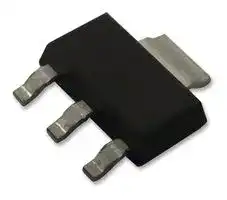
- RF Transistor Case: SOT-89
- Transistor Mounting: Surface Mount
- Power Dissipation Pd: 6W
- Transistor Case Style: SOT-89
- Operating Frequency Max: 1GHz
- Drain Source Voltage Vds: 18V
- Operating Temperature Max: 150°C
- Continuous Drain Current Id: 1.5A
| Delivery and price | |
|---|---|
| Units per pack | 500 |
| Price | 1.76 € |
| Current stock | 10+ |
| Lead time | 30 days |
RF power transistor the LdmoST plastic family

## **PD84001** ~~(S/n~~

## **Features**

- Excellent thermal stability

- Common source configuration

- Broadband performances POUT = 1 W with 15 dB gain @ 870 MHz

- Plastic package

- ESD protection

**==> picture [31 x 8] intentionally omitted <==**

**----- Start of picture text -----**<br>
SOT-89<br>**----- End of picture text -----**<br>


- Supplied in tape and reel

- In compliance with the 2002/95/EC european directive

## **Description**

## **Figure 1. Pin connection**

**==> picture [35 x 9] intentionally omitted <==**

**----- Start of picture text -----**<br>
Source<br>**----- End of picture text -----**<br>


The PD84001 is a common source N-channel, enhancement-mode lateral field-effect RF power transistor. It is designed for high gain, broad band commercial and industrial applications. It operates at 7 V in common source mode at frequencies of up to 1 GHz.

PD84001’s superior gain and efficiency makes it an ideal solution for portable radio and UHF RFID reader.

**==> picture [83 x 21] intentionally omitted <==**

**----- Start of picture text -----**<br>
Source<br>Gate Drain<br>**----- End of picture text -----**<br>


**Table 1. Device summary Order code Marking Package Packaging** PD84001 8401 SOT-89 Tape and reel ~~—[pp]~~

_www.st.com_

1/18

August 2008

Rev 4

**Contents**

**PD84001**

## **Contents**

|**1**|**Electrical data  . . . . . . . . . . . . . . . . . . . . . . . . . . . . . . . . . . . . . . . . . . . . . . 3**|
|---|---|
||1.1<br>Maximum ratings  . . . . . . . . . . . . . . . . . . . . . . . . . . . . . . . . . . . . . . . . . . . . 3|
||1.2<br>Thermal data  . . . . . . . . . . . . . . . . . . . . . . . . . . . . . . . . . . . . . . . . . . . . . . . 3|
|**2**|**Electrical characteristics  . . . . . . . . . . . . . . . . . . . . . . . . . . . . . . . . . . . . . 4**|
||2.1<br>Static  . . . . . . . . . . . . . . . . . . . . . . . . . . . . . . . . . . . . . . . . . . . . . . . . . . . . . 4|
||2.2<br>Dynamic . . . . . . . . . . . . . . . . . . . . . . . . . . . . . . . . . . . . . . . . . . . . . . . . . . . 4|
||2.3<br>ESD protection characteristics . . . . . . . . . . . . . . . . . . . . . . . . . . . . . . . . . . 4|
||2.4<br>Moisture sensitivity level . . . . . . . . . . . . . . . . . . . . . . . . . . . . . . . . . . . . . . . 4|
|**3**|**Impedance  . . . . . . . . . . . . . . . . . . . . . . . . . . . . . . . . . . . . . . . . . . . . . . . . . 5**|
|**4**|**Typical performance . . . . . . . . . . . . . . . . . . . . . . . . . . . . . . . . . . . . . . . . . 6**|
|**5**|**Test circuit . . . . . . . . . . . . . . . . . . . . . . . . . . . . . . . . . . . . . . . . . . . . . . . . 11**|
|**6**|**Package mechanical data . . . . . . . . . . . . . . . . . . . . . . . . . . . . . . . . . . . . 12**|
||6.1<br>Thermal pad and via design . . . . . . . . . . . . . . . . . . . . . . . . . . . . . . . . . . . 14|
||6.2<br>Soldering profile . . . . . . . . . . . . . . . . . . . . . . . . . . . . . . . . . . . . . . . . . . . . 15|
|**7**|**Revision history  . . . . . . . . . . . . . . . . . . . . . . . . . . . . . . . . . . . . . . . . . . . 17**|


2/18

**Electrical data**

**PD84001**

## **1 Electrical data**

## **1.1 Maximum ratings**

**Table 2. Absolute maximum ratings** (TCASE = +25 °C)

|**Symbol**|**Parameter**|**Value**|**Unit**|
|---|---|---|---|
|V(BR)DSS|Drain-source voltage|18|V|
|VGS|Gate-source voltage|-0.5 to +15|V|
|ID|Drain current|1.5|A|
|PDISS|Power dissipation|6|W|
|TJ|Max. operating junction temperature|150|**°**C|
|TSTG|Storage temperature|-65 to +150|**°**C|


## **1.2 Thermal data**

## **Table 3. Thermal data**

|**Symbol**|**Parameter**|**Value**|**Unit**|
|---|---|---|---|
|RthJC|Junction - case thermal resistance|21|**°**C/W|


3/18

**Electrical characteristics**

**PD84001**

## **2 Electrical characteristics**

## **2.1 Static**

**Table 4. Static** (TCASE = +25[o] C)

|**Symbol**|**Test conditions**|**Min.**|**Typ.**|**Max.**|**Unit**|
|---|---|---|---|---|---|
|IDSS|VGS= 0 V<br>VDS= 28 V|||1|μA|
|IGSS|VGS= 5 V<br>VDS= 0 V|||1|μA|
|VGS(Q)|VDS= 10 V<br> ID= 250μA|2.0|3.0|5.0|V|
|VDS(ON)|VGS= 10 V<br>ID= 0.4 A||0.6||V|
|CISS|VGS= 0 V<br>VDS= 7 V<br>f = 1 MHz||14.7||pF|
|COSS|VGS= 0 V<br>VDS= 7 V<br>f = 1 MHz||13.3||pF|
|CRSS|VGS= 0 V<br>VDS= 7 V<br>f = 1 MHz||1.3||pF|


## **2.2 Dynamic**

## **Table 5. Dynamic**

|**Table 5.**|**Dynamic**|||||
|---|---|---|---|---|---|
|**Symbol**|**Test conditions**|**Min.**|**Typ.**|**Max.**|**Unit**|
|POUT|VDD= 7.5 V, IDQ= 50 mA, PIN= 17 dBm, f = 870 MHz|30|31||dBm|
|GPS|VDD= 7.5 V, IDQ= 50 mA, POUT= 30 dBm, f = 870 MHz|13|15||dB|
|hD|VDD= 7.5 V, IDQ= 50 mA PIN= 17 dBm, f = 870 MHz|55|60||%|
|Load<br>mismatch|VDD= 7.5 V, IDQ= 50 mA, POUT= 1 W, f = 870 MHz<br>All phase angles|20:1|||VSWR|


## **2.3 ESD protection characteristics**

## **Table 6. ESD protection characteristics**

|**Table 6.**<br>**ESDprotection characteristics**||
|---|---|
|**Test conditions**|**Class**|
|Human body model|2|
|Machine model|M3|


## **2.4**

## **Moisture sensitivity level**

**Table 7. Moisture sensitivity level**

|**Test methodology**|**Rating**|
|---|---|
|J-STD-020B|MSL 3|


4/18

**PD84001**

**Impedance**

## **3 Impedance**

## **Figure 2. Current conventions**

## **Table 8. Impedance data**

|**Table 8.**<br>**Impedance datapedance dataedance data**|||
|---|---|---|
|**Freq. (MHz)**|**ZGS (**Ω**)**|**ZDL(**Ω**)**|
|920|4.0 + j4.3|3.7 + j6.2|
|900|3.6 + j4.3|3.9 + j5.5|
|880|3.3 + j4.1|4.1 + j4.7|
|860|3.1 + j3.7|4.3 + j4.0|
|840|2.9 + j3.4|4.5 + j3.2|
|820|2.8 + j3.0|4.8 + j2.4|
|800|2.7 + j2.5|5.0 + j1.6|


5/18

**Typical performance**

**PD84001**

## **4 Typical performance**

## **Figure 3. VGS vs ID**

**==> picture [201 x 194] intentionally omitted <==**

## **Figure 4. DC output characteristics**

**==> picture [200 x 195] intentionally omitted <==**

6/18

**Typical performance**

**PD84001**

## **Figure 5. CRSS vs VDS**

## **Figure 6. CISS vs VDS**

**==> picture [462 x 430] intentionally omitted <==**

**----- Start of picture text -----**<br>
3.2 20<br>3.0<br>2.8 18<br>2.6 16<br>2.4<br>2.2 14<br>2.0 12<br>1.8<br>1.6 10<br>1.4<br>8<br>1.2<br>1.0 6<br>0.8<br>0.6 4<br>0.4 2<br>0.2<br>0.0 0<br>0 1 2 3 4 5 6 7 8 9 10 11 12 13 14 15 0 1 2 3 4 5 6 7 8 9 10 11 12 13 14 15<br>CRSS Vds (V)<br>CISS Vds (V)<br>Figure 7. COSS VS VDS<br>Coss vs Vds<br>28<br>26<br>24<br>22<br>20<br>18<br>16<br>14<br>12<br>10<br>8<br>6<br>4<br>2<br>0<br>0 1 2 3 4 5 6 7 8 9 10 11 12 13 14 15<br>COSS Vds (V)<br>Crss (pF) Ciss (pF)<br>Coss (pF)<br>**----- End of picture text -----**<br>


7/18

**Typical performance**

**PD84001**

## **Figure 8. Gain vs output power and frequency**

**Figure 9. Output power vs input power and frequency**

**==> picture [462 x 216] intentionally omitted <==**

**----- Start of picture text -----**<br>
34<br>20<br>32<br>18<br>30<br>16<br>28<br>14<br>26<br>12<br>24<br>10 Vdd = 7.5V<br>22 Idq = 50mA<br>8<br>20<br>6 18<br>18 20 22 24 26 28 30 32 34 0 2 4 6 8 10 12 14 16 18 20<br>Pout (dBm) Pin (dBm)<br>840 MHz 870 MHz 900 MHz 840 MHz 870 MHz 900 MHz<br>Gain (dB) Pout (dBm)<br>**----- End of picture text -----**<br>


## **Figure 10. Efficiency vs output power and frequency**

**Figure 11. Gain and efficiency vs frequency**

**==> picture [462 x 213] intentionally omitted <==**

**----- Start of picture text -----**<br>
70 18 80<br>60 16 70<br>50 14 60<br>40 12 50<br>30 10 40<br>Vdd = 7.5V<br>Idq = 50mA Pin = 17dBm<br>20 8 Vdd = 7.5V 30<br>Idq = 50mA<br>10<br>6 20<br>18 20 22 24 26 28 30 32 34<br>810 820 830 840 850 860 870 880 890 900 910 920<br>Pout (dBm) Freq (MHz)<br>840 MHz 870 MHz 900 MHz Gain Nd<br>Nd (%) Gain (dB)<br>**----- End of picture text -----**<br>


8/18

**Typical performance**

**PD84001**

**Figure 12. Input return loss vs frequency**

**==> picture [219 x 23] intentionally omitted <==**

**----- Start of picture text -----**<br>
Figure 13. Output power vs input power and<br>VDD<br>**----- End of picture text -----**<br>


**==> picture [462 x 228] intentionally omitted <==**

**----- Start of picture text -----**<br>
0 34<br>32<br>Pin = 17dBm<br>-2 Vdd = 7.5V<br>Idq = 50mA 30<br>28<br>-4<br>26<br>-6<br>24<br>Freq = 870 MHz<br>22 Idq = 50mA<br>-8<br>20<br>-10 18<br>810 820 830 840 850 860 870 880 890 900 910 920 0 2 4 6 8 10 12 14 16 18 20<br>Freq (MHz) Pin (dBm)<br>9V 7.5V 6V<br>Pout (dBm)<br>Input Return Loss (dB)<br>**----- End of picture text -----**<br>


**Figure 14. Efficiency vs output power and VDD Figure 15. Output power and drain current vs drain supply voltage**

**==> picture [462 x 236] intentionally omitted <==**

**----- Start of picture text -----**<br>
70 34 0.6<br>Freq = 870 MHz<br>60 32 Pin = 17dBm 0.5<br>Idq = 50mA<br>50 30 0.4<br>40 28 0.3<br>30 26 0.2<br>20 24 0.1<br>10 22 0<br>18 20 22 24 26 28 30 32 34<br>2 3 4 5 6 7 8 9 10<br>Pout (dBm)<br>Vdd (V)<br>9V 7.5V 6V<br>Pout ID<br>Nd (%)<br>Pout (dBm)<br>**----- End of picture text -----**<br>


9/18

**Typical performance**

**PD84001**

**==> picture [462 x 287] intentionally omitted <==**

**----- Start of picture text -----**<br>
Figure 16. Gain and efficiency vs pin<br>y<br>26 90<br>24 80<br>22 70<br>20 60<br>Freq = 520 MHz<br>18 50<br>Vdd = 7.5V<br>16 40<br>14 30<br>12 20<br>10 10<br>8 0<br>-5 0 5 10 15 20 25 30<br>Pin (dBm)<br>Gain-70mA Gain-200mA Gain-50mA Gain-100mA<br>Eff-70mA Eff-200mA Eff-50mA Eff-100mA<br>Gain (dB)<br>Efficiency (%)<br>**----- End of picture text -----**<br>


10/18

**Test circuit**

**PD84001**

## **5 Test circuit**

## **Figure 17. Test circuit schematic / 840-900 MHz**

11/18

**Package mechanical data**

**PD84001**

## **6 Package mechanical data**

In order to meet environmental requirements, ST offers these devices in ECOPACK® packages. These packages have a lead-free second level interconnect . The category of second level interconnect is marked on the package and on the inner box label, in compliance with JEDEC Standard JESD97. The maximum ratings related to soldering conditions are also marked on the inner box label. ECOPACK is an ST trademark. ECOPACK specifications are available at: www.st.com

12/18

**Package mechanical data**

**PD84001**

**Table 9. SOT-89 mechanical data**

|**Dim.**|**mm.**|**mm.**|**mm.**|**Inch**|**Inch**|**Inch**|
|---|---|---|---|---|---|---|
||**Min**|**Typ**|**Max**|**Min**|**Typ**|**Max**|
|A<br>~~a~~<br>~~a~~|1.4<br>~~a~~<br>~~i~~|~~ee~~<br>~~ee~~|1.6<br>~~es~~|55.1||63.0|
|B<br>~~a ~~<br>~~a~~|0.44<br> ~~a ~~<br>~~i~~|~~ee~~<br>~~ee~~<br>~~ee es~~|0.56<br>~~es~~<br>~~es~~|17.3<br>~~ee~~|~~ee~~|22.0|
|B1<br>~~a ~~<br>~~es~~|0.36<br> ~~i~~<br>~~es~~|~~ee ~~<br>~~es~~<br>~~ee es~~|0.48<br> ~~es~~<br>~~es~~<br>~~es~~|14.2<br>~~es~~<br>~~ee~~|~~es~~<br>~~ee~~|18.9<br>~~es~~|
|C<br>~~es~~<br>~~ee~~<br>~~Po~~|0.35<br>~~es~~<br>~~ee~~|~~es~~<br>~~ee es~~<br>~~ee~~|0.44<br>~~es~~<br>~~es ~~<br>~~ee~~|13.8<br>~~es~~<br> ~~ee~~<br>~~ee~~|~~es~~<br>~~ee~~<br>~~ee~~|17.3<br>~~es~~<br>~~ee~~|
|C1<br>~~ee~~<br>~~Po~~<br>~~po~~|0.35<br>~~ee~~|~~ee~~|0.44<br>~~ee~~|13.8<br>~~ee~~|~~ee~~|17.3<br>~~ee~~|
|D<br>~~Po~~<br>~~po~~<br>~~po~~|4.4||4.6|173.2||181.1|
|D1<br>~~po~~<br>~~po~~<br>~~a~~|1.62<br>~~i~~|~~ee~~|1.83<br>~~es~~|63.8||72.0|
|E<br>~~po~~<br>~~a~~|2.29<br>~~i~~|~~ee~~<br>~~ee es~~|2.6<br>~~es~~<br>~~es~~|90.2<br>~~ee~~|~~ee~~|102.4|
|e<br>~~a ~~<br>~~es~~|1.42<br> ~~i~~<br>~~es~~|~~ee ~~<br>~~es~~<br>~~ee es~~|1.57<br> ~~es~~<br>~~es~~<br>~~es~~|55.9<br>~~es~~<br>~~ee~~|~~es~~<br>~~ee~~|61.8<br>~~es~~|
|e1<br>~~es~~<br>~~ee~~<br>~~Po~~|2.92<br>~~es~~<br>~~ee~~|~~es~~<br>~~ee es~~<br>~~ee~~|3.07<br>~~es~~<br>~~es ~~<br>~~ee~~|115.0<br>~~es~~<br> ~~ee~~<br>~~ee~~|~~es~~<br>~~ee~~<br>~~ee~~|120.9<br>~~es~~<br>~~ee~~|
|H<br>~~ee~~<br>~~Po~~<br>~~po~~|3.94<br>~~ee~~|~~ee~~|4.25<br>~~ee~~|155.1<br>~~ee~~|~~ee~~|167.3<br>~~ee~~|
|L<br>~~Po~~<br>~~po~~|0.89||1.2|35.0||47.2|


## **Figure 18. Package dimensions**

13/18

**Package mechanical data**

**PD84001**

## **6.1 Thermal pad and via design**

Thernal vias are required in the PCB layout to effectively conduct heat away from the package. The via pattern has been designed to address thermal, power dissipation and electrical requirements of the device.

The via pattern is based on thru-hole vias with 0.203 mm to 0.330 mm finished hole size on a 0.5 mm to 1.2 mm grid pattern with 0.025 plating on via walls. If micro vias are used in a design, it is suggested that the quantity of vias be increased by a 4:1 ratio to achieve similar results.

## **Figure 19. Pad layout details**

**==> picture [31 x 8] intentionally omitted <==**

**----- Start of picture text -----**<br>
SOT-89<br>**----- End of picture text -----**<br>


14/18

**Package mechanical data**

**PD84001**

## **6.2 Soldering profile**

_Figure 20_ shows the recommeded solder for devices that have Pb-free terminal plating and where a Pb-free solder is used.

## **Figure 20. Recommended solder profile**

_Figure 21_ shows the recommeded solder for devices with Pb-free terminal plating used with leaded solder, or for devices with leaded terminal plating used with a leaded solder.

**Figure 21. Recommended solder profile for leaded devices**

15/18

**Package mechanical data**

**PD84001**

## **Figure 22. Reel information**

**==> picture [405 x 395] intentionally omitted <==**

16/18

**Revision history**

**PD84001**

## **7 Revision history**

## **Table 10. Document revision history**

|**Date**|**Revision**|**Changes**|
|---|---|---|
|06-Dec-2006|1|Initial release|
|16-May-2007|2|Marking updated|
|05-Jun-2007|3|Part number update|
|25-Aug-2008|4|Updated_Table 4 on page 4_|


17/18

**PD84001**

## **Please Read Carefully:**

Information in this document is provided solely in connection with ST products. STMicroelectronics NV and its subsidiaries (“ST”) reserve the right to make changes, corrections, modifications or improvements, to this document, and the products and services described herein at any time, without notice.

All ST products are sold pursuant to ST’s terms and conditions of sale.

Purchasers are solely responsible for the choice, selection and use of the ST products and services described herein, and ST assumes no liability whatsoever relating to the choice, selection or use of the ST products and services described herein.

No license, express or implied, by estoppel or otherwise, to any intellectual property rights is granted under this document. If any part of this document refers to any third party products or services it shall not be deemed a license grant by ST for the use of such third party products or services, or any intellectual property contained therein or considered as a warranty covering the use in any manner whatsoever of such third party products or services or any intellectual property contained therein.

**UNLESS OTHERWISE SET FORTH IN ST’S TERMS AND CONDITIONS OF SALE ST DISCLAIMS ANY EXPRESS OR IMPLIED WARRANTY WITH RESPECT TO THE USE AND/OR SALE OF ST PRODUCTS INCLUDING WITHOUT LIMITATION IMPLIED WARRANTIES OF MERCHANTABILITY, FITNESS FOR A PARTICULAR PURPOSE (AND THEIR EQUIVALENTS UNDER THE LAWS OF ANY JURISDICTION), OR INFRINGEMENT OF ANY PATENT, COPYRIGHT OR OTHER INTELLECTUAL PROPERTY RIGHT.**

**UNLESS EXPRESSLY APPROVED IN WRITING BY AN AUTHORIZED ST REPRESENTATIVE, ST PRODUCTS ARE NOT RECOMMENDED, AUTHORIZED OR WARRANTED FOR USE IN MILITARY, AIR CRAFT, SPACE, LIFE SAVING, OR LIFE SUSTAINING APPLICATIONS, NOR IN PRODUCTS OR SYSTEMS WHERE FAILURE OR MALFUNCTION MAY RESULT IN PERSONAL INJURY, DEATH, OR SEVERE PROPERTY OR ENVIRONMENTAL DAMAGE. ST PRODUCTS WHICH ARE NOT SPECIFIED AS "AUTOMOTIVE GRADE" MAY ONLY BE USED IN AUTOMOTIVE APPLICATIONS AT USER’S OWN RISK.**

Resale of ST products with provisions different from the statements and/or technical features set forth in this document shall immediately void any warranty granted by ST for the ST product or service described herein and shall not create or extend in any manner whatsoever, any liability of ST.

ST and the ST logo are trademarks or registered trademarks of ST in various countries.

Information in this document supersedes and replaces all information previously supplied.

The ST logo is a registered trademark of STMicroelectronics. All other names are the property of their respective owners.

© 2008 STMicroelectronics - All rights reserved

STMicroelectronics group of companies

Australia - Belgium - Brazil - Canada - China - Czech Republic - Finland - France - Germany - Hong Kong - India - Israel - Italy - Japan - Malaysia - Malta - Morocco - Singapore - Spain - Sweden - Switzerland - United Kingdom - United States of America

**www.st.com**

18/18
Updated at February 9, 2023
STMicroelectronics is a global leader in the semiconductor industry, recognized for developing highly integrated, energy-efficient solutions that power modern electronics. With a strong focus on innovation, ST provides a comprehensive portfolio of microelectronics that address the demanding requirements of industrial, automotive, communications, and consumer applications. Our extensive selection of STMicroelectronics components is built around a robust lineup of discrete semiconductors and circuit protection devices. We offer a wide variety of single MOSFETs, Schottky diodes, and fast and ultrafast recovery rectifier diodes, designed to deliver exceptional efficiency and thermal performance in power management and conversion systems. For robust circuit protection, our inventory features hundreds of transient voltage suppressors and TVS diodes that safeguard sensitive electronic components against destructive voltage spikes. In addition to core power discretes like TRIACs, SCRs, bipolar transistors, and single IGBTs, our STMicroelectronics range includes specialized integrated passive filters and MEMS sensors. Furthermore, ST offers advanced integrated passive devices, such as baluns and RF filters, which utilize high-quality monolithic RF IPD processes on glass or high-resistance silicon substrates. These components provide competitive cost structures, reduced power losses, and simplified RFIC-to-antenna matching, ensuring optimal system performance and delivering the reliability required for next-generation wireless and power designs.
About Novapart
Novapart is a B2B electronic component broker specialising in stock shortages and cost reduction. We source hard-to-find parts and identify compliant alternatives across a catalogue of 540,000+ components from 500+ manufacturers.
Learn more →Stock Shortage Specialist
When a component is unavailable, discontinued or has an unacceptable lead time, we tap into our network of vetted European and Asian distributors to source what you need — without compromising on quality or traceability.
Request a quote →Compliant Alternatives
We identify pin-to-pin, electrically equivalent substitutes that meet the same certifications (RoHS, AEC-Q100, REACH) as your original specification — validated against datasheets, not just part numbers. Often at a lower cost.
BOM Analysis service →