
Image not available
Illustrative purposes only

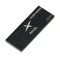
PCS.55.M
RF Antenna, 2.5 to 2.69GHz, 5G/4G/LTE/GPS/GNSS/Glonass/Galileo/BeiDou/CAT-M/NB-IoT/IoT, 0dBi, 50 ohm
⚠️ Reference pricing provided. In case of supply shortages, we will connect you with our trusted procurement partners to ensure your project's continuity.
- Manufacturer: TAOGLAS
- Product type:
- Gain: 0dBi
- SVHC: To Be Advised
- VSWR: -
- Input Power: 2W
- Antenna Type: 5G / 4G / LTE / GPS / GNSS / Glonass / Galileo / BeiDou / CAT-M / NB-IoT / IoT
- Frequency Max: 2.69GHz
- Frequency Min: 2.5GHz
- Product Range: -
- Input Impedance: 50ohm
- Antenna Mounting: SMD
- Antenna Polarisation: Linear
| Delivery and price | |
|---|---|
| Units per pack | 500 |
| Price | 1.25 € |
| Current stock | 500+ |
| Lead time | 30 days |
Datasheet

## AS ~ a“ > \ TAOGLAS. + 5 Qd om Y) (© +) (O C) **Part No: PCS.55.M** **Description** Small OTS LTE Antenna 600-3000 MHz **Features:** Small form factor SMD Dielectric Antenna 5G/4G/LTE: 600-3000MHz GPS / GLONASS / Galileo / BeiDou (1561-1602MHz) Available in North America (NA), European Union (EMEA), and World Wide (WW) configurations Dimensions: 27*10*1.6mm RoHS & REACH Compliant SPE-23-8-281-A www.taoglas.com **==> picture [358 x 270] intentionally omitted <==** **----- Start of picture text -----**<br> 1. Introduction 2<br>2. Specifications 3<br>3. Antenna Characteristics 6<br>4. Radiation Patterns 9<br>5. Mechanical Drawing 46<br>6. Packaging 47<br>7. Antenna Integration Guide 48<br>8. Application Note 59<br>9 Solder Reflow Profile 69<br>Changelog 70<br>**----- End of picture text -----**<br> Taoglas makes no warranties based on the accuracy or completeness of the contents of this document and reserves the right to make changes to specifications and product descriptions at any time without notice. Taoglas reserves all rights to this document and the information contained herein. Reproduction, use or disclosure to third parties without express permission is strictly prohibited. 1 www.taoglas.com SPE-23-8-281-A The PCS.55.M, is a patent pending compact cellular antenna designed specifically for IoT devices with small ground planes. It combines revolutionary antenna design techniques with the antenna integration experience of Taoglas to provide a solution for wideband coverage of both 5G/4G LTE and GNSS bands, including the most challenging 600700MHz bands. The PCS.55.M provides a simple off-the-shelf solution for LTE, LTE CAT-M, NB-IoT, & GNSS applications. At only 27x10x1.6mm, this compact cellular antenna is the perfect antenna for small IoT devices, where requirements for smaller PCB design are becoming more dependent on the antenna size. This antenna also has a relatively small keepout area compared to most other compact cellular antennas that are on the market, owing to Taoglas' years of antenna design expertise. Typical Applications include: - Handheld IoT Devices - Handsets and Tablets - Compact Asset Trackers The PCS.55.M is available in three matching configurations. The optimum components for North America (NA), European Union (EU), and World Wide (WW) have been determined to allow designers to easily integrate the PCS.55.M to get the best performance for any particular deployment scenario. The PCS.55.M is easy to integrate using standard SMD technologies and the matching circuits for each deployment (NA, EMEA, or WW) have been simplified to a 3 component configuration to allow for greater flexibility on the user side. Many antennas advertise a small form factor but with the hidden cost of implementing a large PCB ground plane. At Taoglas, we believe that the whole antenna system (antenna + ground plane) needs to be small to meet the evolving demands of the IoT market. As a result, we have performed experimental ground plane studies in order to be fully transparent on the effect of small ground planes on antenna performance. This allows our customers to have full visibility on how our antennas will perform on various different ground plane sizes. The data for these studies is shown in the Application Note on page 59. For further information or, integration and matching guidelines contact your regional Taoglas customer support team. 2 www.taoglas.com SPE-23-8-281-A |**Electrical**|**Electrical**|**Electrical**|**Electrical**|**Electrical**|**Electrical**|**Electrical**|**Electrical**|**Electrical**|**Electrical**|**Electrical**| |---|---|---|---|---|---|---|---|---|---|---| |**Band**|Frequency<br>(MHz)|Measurement|Measurement<br>Efficiency (%)|Average Gain<br>(dB)|Peak Gain<br>(dBi)|Return Loss<br>(dB)|Impedance|Polarization|Radiation<br>Pattern|Max Input<br>Power| |**5GNR**<br>**Band71**|617-698|NA|17.9|-7.5|-4.4|-2.5|50 Ω|Linear|Omni|2W| |||EMEA|9.1|-10.4|-7.3|-2.5||||| |||WW|23.9|-6.2|-3.3|-4.7||||| |**5GNR/4G**<br>**Band 12,17,28,29,85**|698-746|NA|47.4|-3.2|0.2|-8.5||||| |||EMEA|23.3|-6.3|-2.7|-4.1||||| |||WW|31.2|-5.1|-1.6|-3.7||||| |**5GNR/4G**<br>**Band 13,14,20,28**|746-800|NA|41.7|-3.8|-0.3|-5.1||||| |||EMEA|31.1|-5.1|-1.5|-4.4||||| |||WW|31.7|-5.0|-1.5|-3.3||||| |**5GNR/4G**<br>**Band**<br>**5,18,19,20,26,27**|800-880|NA|27.4|-5.6|-2.2|-3.1||||| |||EMEA|35.6|-4.5|-1.0|-5.0||||| |||WW|32.6|-4.9|-1.6|-4.1||||| |**5GNR/4G**<br>**Band 5,8,19,26**|880-960|NA|16.1|-7.9|-4.4|-2.6||||| |||EMEA|26.6|-5.7|-1.8|-5.6||||| |||WW|23.6|-6.3|-2.6|-4.3||||| |**5GNR/4G**<br>**Band 74,75,76**|1427-1518|NA|32.9|-4.8|0.4|-4.7||||| |||EMEA|24.8|-6.1|-1.0|-3.1||||| |||WW|31.9|-5.0|0.4|-5.0||||| |**GNSS**|1560-1602|NA|43.3|-3.6|1.2|-5.9||||| |||EMEA|35.2|-4.5|0.7|-4.7||||| |||WW|43.3|-3.6|1.6|-6.3||||| |**4G/3G**<br>**Band**<br>**1,2,3,4,25,39,66**|1710-2155|NA|46.6|-3.3|3.7|-6.3||||| |||EMEA|47.4|-3.2|3.3|-6.6||||| |||WW|43.0|-3.7|3.5|-5.9||||| |**4G/3G**<br>**Band 7, 38, 41, 69**|2500-2690|NA|14.7|-8.3|-2.0|-1.8||||| |||EMEA|20.9|-6.8|-0.4|-2.2||||| |||WW|18.6|-7.3|0.0|-2.2||||| The PCS.55.M antenna performance was measured with Taoglas PCSD.55.A EVB. 3 www.taoglas.com SPE-23-8-281-A ||**Mechanical**| |---|---| |Antenna Dimensions|27 x 10 x 1.6mm| |Material|FR4| |Weight|0.9g| |Soldering Type|SMD| ||**Environmental**| |---|---| |Operation Temperature|-40°C ~ +85°C| |Storage Temperature|-40°C ~ +85°C| |Moisture Sensitivity Level|3| 4 www.taoglas.com SPE-23-8-281-A |||**5G/4G Bands**|**5G/4G Bands**|**5G/4G Bands**|| |---|---|---|---|---|---| |**Band Number**||**5GNR/ FR1/ LTE/ LTE-Advanced/ WCDMA/ HSPA/ HSPA+/ TD-SCDMA**|||| ||**Uplink**|**Downlink**|**EMEA**|**NA**|**WW**| |**B1**|1920 to 1980|2110 to 2170|✓|✓|✓| |**B2**|1850 to 1910|1930 to 1990|✓|✓|✓| |**B3**|1710 to 1785|1805 to 1880|✓|✓|✓| |**B4**|1710 to 1755|2110 to 2155|✓|✓|✓| |**B5**|824 to 849|869 to 894|✓|✓|✓| |**B7**|2500 to 2570|2620 to 2690|✓||✓| |**B8**|880 to 915|925 to 960|✓|✓|✓| |**B9**|1749.9 to 1784.9|1844.9 to 1879.9|✓|✓|✓| |**B11**|1427.9 to 1447.9|1475.9 to 1495.9|✓|✓|✓| |**B12**|699 to 716|729 to 746||✓|✓| |**B13**|777 to 787|746 to 756|✓|✓|✓| |**B14**|788 to 798|758 to 768|✓|✓|✓| |**B17**|704 to 716|734 to 746||✓|✓| |**B18**|815 to 830|860 to 875|✓|✓|✓| |**B19**|830 to 845|875 to 890|✓|✓|✓| |**B20**|832 to 862|791 to 821|✓|✓|✓| |**B21**|1447.9 to 1462.9|1495.9 to 1510.9|✓|✓|✓| |**B22**|3410 to 3490|3510 to 3590|||| |**B23**|2000 to 2020|2180 to 2200|✓|✓|✓| |**B24**|1626.5 to 1660.5|1525 to 1559|✓|✓|✓| |**B25**|1850 to 1915|1930 to 1995|✓|✓|✓| |**B26**|814 to 849|859 to 894|✓|✓|✓| |**B27**|807 to 824|852 to 869|✓|✓|✓| |**B28**|703 to 748|758 to 803|✓|✓|✓| |**B29**|717 t|o 728|✓|✓|✓| |**B30**|2305 to 2315|2350 to 2360|✓|✓|✓| |**B31**|452.5 to 457.5|462.5 to 467.5|||| |**B32**|1452 t|o 1496|✓|✓|✓| |**B34**|2010 t|o 2025|✓|✓|✓| |**B35**|1850 t|o 1910|✓|✓|✓| |**B36**|1930 t|o 1990|✓|✓|✓| |**B37**|1910 t|o 1930|✓|✓|✓| |**B38**|2570 t|o 2620|✓||✓| |**B39**|1880 t|o 1920|✓|✓|✓| |**B40**|2300 t|o 2400|✓|✓|✓| |**B41**|2496 t|o 2690|✓||✓| |**B42**|3400 t|o 3600|||| |**B43**|3600 t|o 3800|||| |**B45**|1447 t|o 1467|✓|✓|✓| |**B46**|5150 t|o 5925|||| |**B47**|5855 t|o 5925|||| |**B48**|3550 t|o 3700|||| |**B49**|3550 t|o 3700|||| |**B50**|1432 t|o 1517|✓|✓|✓| |**B51**|1427 t|o 1432|✓|✓|✓| |**B52**|3300 t|o 3400|||| |**B53**|2483.5|to 2495|✓||✓| |**B65**|1920 to 2010|2110 to 2200|✓|✓|✓| |**B66**|1710 to 1780|2110 to 2200|✓|✓|✓| |**B68**|698 to 728|753 to 783|✓|✓|✓| |**B69**|2570 t|o 2620|✓||✓| |**B70**|1695 to 1710|1995 to 2020|✓|✓|✓| |**B71**|663 to 698|617 to 652|||✓| |**B72**|451 to 456|461 to 466|||| |**B73**|450 to 455|460 to 465|||| |**B74**|1427 to 1470|1475 to 1518|✓|✓|✓| |**B75**|1432 t|o 1517|✓|✓|✓| |**B76**|1427 t|o 1432|✓|✓|✓| |**B77**|3300 t|o 4200|||| |**B78**|3300 t|o 3800|||| |**B79**|4400 t|o 5000|||| |**B85**|698 to 716|728 to 746||✓|✓| |**B87**|410 to 415|420 to 425|||| |**B88**|412 to 417|422 to 427|||| 5 www.taoglas.com SPE-23-8-281-A ## Return Loss ## VSWR 6 www.taoglas.com SPE-23-8-281-A ## **3.3** Efficiency ff ## **3.4** Average Gain ff 7 www.taoglas.com SPE-23-8-281-A ## **3.5** Peak Gain | 8 www.taoglas.com SPE-23-8-281-A ## Test Setup 9 www.taoglas.com SPE-23-8-281-A ## EMEA Patterns at 650 MHz ## XZ Plane ## YZ Plane ## XY Plane 10 www.taoglas.com SPE-23-8-281-A ## NA Patterns at 650 MHz ## XZ Plane ## YZ Plane ## XY Plane 11 www.taoglas.com SPE-23-8-281-A ## WW Patterns at 650 MHz ## XZ Plane ## YZ Plane ## XY Plane 12 www.taoglas.com SPE-23-8-281-A ## EMEA Patterns at 700 MHz ## XZ Plane ## YZ Plane ## XY Plane 13 www.taoglas.com SPE-23-8-281-A ## NA Patterns at 700 MHz ## XZ Plane ## YZ Plane ## XY Plane 14 www.taoglas.com SPE-23-8-281-A ## WW Patterns at 700 MHz ## XZ Plane ## YZ Plane ## XY Plane 15 www.taoglas.com SPE-23-8-281-A ## EMEA Patterns at 850 MHz ## XZ Plane ## YZ Plane ## XY Plane 16 www.taoglas.com SPE-23-8-281-A ## NA Patterns at 850 MHz ## XZ Plane ## YZ Plane ## XY Plane 17 www.taoglas.com SPE-23-8-281-A ## WW Patterns at 850 MHz ## XZ Plane ## YZ Plane ## XY Plane 18 www.taoglas.com SPE-23-8-281-A ## EMEA Patterns at 900 MHz ## XZ Plane ## YZ Plane ## XY Plane 19 www.taoglas.com SPE-23-8-281-A ## NA Patterns at 900 MHz ## XZ Plane ## YZ Plane ## XY Plane 20 www.taoglas.com SPE-23-8-281-A ## WW Patterns at 900 MHz ## XZ Plane ## YZ Plane ## XY Plane 21 www.taoglas.com SPE-23-8-281-A ## EMEA Patterns at 960 MHz ## XZ Plane ## YZ Plane ## XY Plane 22 www.taoglas.com SPE-23-8-281-A ## NA Patterns at 960 MHz ## XZ Plane ## YZ Plane ## XY Plane 23 www.taoglas.com SPE-23-8-281-A ## WW Patterns at 960 MHz ## XZ Plane ## YZ Plane ## XY Plane 24 www.taoglas.com SPE-23-8-281-A ## EMEA Patterns at 1450 MHz ## XZ Plane ## YZ Plane ## XY Plane 25 www.taoglas.com SPE-23-8-281-A ## NA Patterns at 1450 MHz ## XZ Plane ## YZ Plane ## XY Plane 26 www.taoglas.com SPE-23-8-281-A ## WW Patterns at 1450 MHz ## XZ Plane ## YZ Plane ## XY Plane 27 www.taoglas.com SPE-23-8-281-A ## EMEA Patterns at 1575 MHz ## XZ Plane ## YZ Plane ## XY Plane 28 www.taoglas.com SPE-23-8-281-A ## NA Patterns at 1575 MHz ## XZ Plane ## YZ Plane ## XY Plane 29 www.taoglas.com SPE-23-8-281-A ## WW Patterns at 1575 MHz ## XZ Plane ## YZ Plane ## XY Plane 30 www.taoglas.com SPE-23-8-281-A ## EMEA Patterns at 1710 MHz ## XZ Plane ## YZ Plane ## XY Plane 31 www.taoglas.com SPE-23-8-281-A ## NA Patterns at 1710 MHz ## XZ Plane ## YZ Plane ## XY Plane 32 www.taoglas.com SPE-23-8-281-A ## WW Patterns at 1710 MHz ## XZ Plane ## YZ Plane ## XY Plane 33 www.taoglas.com SPE-23-8-281-A ## EMEA Patterns at 1850 MHz ## XZ Plane ## YZ Plane ## XY Plane 34 www.taoglas.com SPE-23-8-281-A ## NA Patterns at 1850 MHz ## XZ Plane ## YZ Plane ## XY Plane 35 www.taoglas.com SPE-23-8-281-A ## WW Patterns at 1850 MHz ## XZ Plane ## YZ Plane ## XY Plane 36 www.taoglas.com SPE-23-8-281-A ## EMEA Patterns at 1910 MHz ## XZ Plane ## YZ Plane ## XY Plane 37 www.taoglas.com SPE-23-8-281-A ## NA Patterns at 1910 MHz ## XZ Plane ## YZ Plane ## XY Plane 38 www.taoglas.com SPE-23-8-281-A ## WW Patterns at 1910 MHz ## XZ Plane ## YZ Plane ## XY Plane 39 www.taoglas.com SPE-23-8-281-A ## EMEA Patterns at 2155 MHz ## XZ Plane ## YZ Plane ## XY Plane 40 www.taoglas.com SPE-23-8-281-A ## NA Patterns at 2155 MHz ## XZ Plane ## YZ Plane ## XY Plane 41 www.taoglas.com SPE-23-8-281-A ## WW Patterns at 2155 MHz ## XZ Plane ## YZ Plane ## XY Plane 42 www.taoglas.com SPE-23-8-281-A ## EMEA Patterns at 2700 MHz ## XZ Plane ## YZ Plane ## XY Plane 43 www.taoglas.com SPE-23-8-281-A ## NA Patterns at 2700 MHz ## XZ Plane ## YZ Plane ## XY Plane 44 www.taoglas.com SPE-23-8-281-A ## WW Patterns at 2700 MHz ## XZ Plane ## YZ Plane ## XY Plane 45 www.taoglas.com SPE-23-8-281-A 46 www.taoglas.com SPE-23-8-281-A 47 www.taoglas.com SPE-23-8-281-A 48 www.taoglas.com SPE-23-8-281-A ## **7.1** Schematic and Symbol Definition ay The circuit symbol for the antenna is shown below. The antenna has 5 pins with only two pins (Pin 1 and Pin 2) as functional. Pins 3, 4 and 5 are for mechanical strength. |**Pin**<br>~~i~~|**Description**<br>~~i~~| |---|---| |1|RF Feed| |2|Ground| |3, 4, 5|Mechanical, Not Connected| 49 www.taoglas.com SPE-23-8-281-A ## Antenna Integration For any given PCB size, the antenna should ideally be placed on the PCB’s shortest side, to take advantage of the ground plane. Optimized matching components can be placed as shown. ## PCB Layout - NA The footprint and clearance on the PCB must meet the layout drawing in section (Footprint Drawing). Note the placement of the optimized components. L1 is placed as close as possible to the RF feed (pad 1) within the copper keep out area. C1 is then placed tightly in series with C2 placed in parallel after that. 50 www.taoglas.com SPE-23-8-281-A ## PCB Layout - EMEA The footprint and clearance on the PCB must meet the layout drawing in section (Footprint Drawing). Note the placement of the optimized components. C1 is placed as close as possible to the RF feed (pad 1) across the copper keep out area. L1 is then placed tightly in parallel with C2 placed in series after that. ## PCB Layout - WW The footprint and clearance on the PCB must meet the layout drawing in section (Footprint Drawing). Note the placement of the optimized components. L1 is placed as close as possible to the RF feed (pad 1) within the copper keep out area. C1 is then placed tightly in series with L2 placed in parallel after that. **==> picture [5 x 11] intentionally omitted <==** **----- Start of picture text -----**<br> c<br>**----- End of picture text -----**<br> 51 www.taoglas.com SPE-23-8-281-A ## PCB Clearance Below shows the antenna footprint and clearance through ALL layers on the PCB. Only the antenna pads and connections to feed and GND are present within this clearance area (marked RED). The clearance area extends to 5.4mm from the antenna pads to the ground area. This clearance area includes the bottom side and ALL internal layers on the PCB. 52 www.taoglas.com SPE-23-8-281-A ## Evaluation Board . 30mm **==> picture [41 x 9] intentionally omitted <==** **----- Start of picture text -----**<br> 120mm<br>**----- End of picture text -----**<br> Topside Bottom Side 53 www.taoglas.com SPE-23-8-281-A ## Evaluation Board Ground Plane Length Ground Plane Length: 103.8mm 54 www.taoglas.com SPE-23-8-281-A ## **7.9** Matching Circuit - NA eed Matching components with the PCS.55.M are recommended for the antenna to have optimal performance on the evaluation board, located in the spaces specified in the above images. Additional matching components may be necessary for your device, so we recommend incorporating extra component footprints, forming a “pi” network, between the cellular module and the edge of the ground plane. |**Designator**|**Type**|**Value**|**Manufacturer**|**Manufacturer Part Number**| |---|---|---|---|---| |L1|Inductor|8.2nH|Murata|LQG15HS8N2G02D| |C1|Capacitor|2.7pF|Murata|GCM1555C1H2R7BA16D| |C2|Capacitor|0.5pF|Murata|GRM1555C1HR50CA01D| 55 www.taoglas.com SPE-23-8-281-A ## Matching Circuit - EMEA Matching components with the PCS.55.M are recommended for the antenna to have optimal performance on the evaluation board, located in the spaces specified in the above images. Additional matching components may be necessary for your device, so we recommend incorporating extra component footprints, forming a “pi” network, between the cellular module and the edge of the ground plane. |**Designator**<br>L1|**Type**<br>Inductor|**Value**<br>10nH|**Manufacturer**<br>TDK|**Manufacturer Part Number**<br>MLK1005S10NJT000| |---|---|---|---|---| |C1|Capacitor|4.3pF|Murata|GJM1555C1H4R3BB01D| |C2|Capacitor|3.3pF|Murata|GJM1555C1H3R3BB01D| 56 www.taoglas.com SPE-23-8-281-A ## **7.11** Matching Circuit - WW ones Matching components with the PCS.55.M are recommended for the antenna to have optimal performance on the evaluation board, located in the spaces specified in the above images. Additional matching components may be necessary for your device, so we recommend incorporating extra component footprints, forming a “pi” network, between the cellular module and the edge of the ground plane. |**Designator**<br>L1|**Type**<br>Inductor|**Value**<br>10nH|**Manufacturer**<br>Murata|**Manufacturer Part Number**<br>MLK1005S10NJT000| |---|---|---|---|---| |L2|Inductor|15nH|Murata|MLK1005S15NJT000| |C1|Capacitor|2.2pF|Murata|GRM1555C1H2R2CA01D| 57 www.taoglas.com SPE-23-8-281-A ## Footprint 58 www.taoglas.com SPE-23-8-281-A The effect of shortening the ground plane on antenna performance was evaluated. Using the evaluation board of the PCS.55.M, the PCB was cut back 10mm at a time and tested in an anechoic chamber. The results for North America (NA), Europe, Middle East, Africa (EMEA), and Worldwide (WW) are shown here: ## Efficiency – North America ## Average Gain – North America 59 www.taoglas.com SPE-23-8-281-A ## **8.3** Peak Gain – North America | ## **8.4** Efficiency – EMEA ff 60 www.taoglas.com SPE-23-8-281-A ## **8.5** Average Gain – EMEA ay ## **8.6** Peak Gain – EMEA es 61 www.taoglas.com SPE-23-8-281-A ## **8.7** Efficiency – Worldwide ff ## **8.8** Average Gain – Worldwide ay 62 www.taoglas.com SPE-23-8-281-A ## Peak Gain – Worldwide 63 www.taoglas.com SPE-23-8-281-A ## Effects of Right Side PCB Ground on Antenna Performance The PCS.55.M antenna was tuned for a 120x80mm ground plane and the distance between the PCB ground on the right side of the antenna was parameterized and swept from 0 to 50 mm. The minimum condition, or 0mm, has the ground right up against the antenna and the maximum condition, or 50mm, has no ground on the right side of the antenna (i.e. a full 80x16mm keep out area). This was done in order to determine the minimum distance that the ground can be placed next to the antenna without affecting performance. The configuration with 25mm is shown below. For minimal (0.2 dB) performance impact, a clearance of 25mm is recommended. Return loss and efficiency 25, 35 and 50mm clearance are shown below: 64 www.taoglas.com SPE-23-8-281-A ## Return Loss ## **8.10.2** Efficiency 65 www.taoglas.com SPE-23-8-281-A ## **8.10.3** Return Loss For more compact designs, a distance of 5 or 10mm can be implemented at the cost of efficiency and bandwidth as shown below: ## Efficiency 66 www.taoglas.com SPE-23-8-281-A ## **8.11** Correlation of CST Blackbox Model to Measured Results To evaluate the accuracy of the CST Blackbox Model available to all customers, the following comparisons of return loss and efficiency have been made: Please note the following simulated results were run at 18 cells/wavelength and with a -80 dB accuracy criterion. The measured results are for the PCS.55.M evaluation board with the NA tuning in place. **==> picture [364 x 10] intentionally omitted <==** **----- Start of picture text -----**<br> v<br>**----- End of picture text -----**<br> 67 www.taoglas.com SPE-23-8-281-A ## Repeatability Study In order to verify the repeatability of the design, 20 production samples of the evaluation board for the PCS.55.M were tested in an anechoic chamber on the same day with standard SMA torque of 1 N ⋅ m 68 www.taoglas.com SPE-23-8-281-A The PCS.55.M can be assembled by following the recommended soldering temperatures are as follows: - *Temperatures listed within a tolerance of +/- 10º C The PCS.55.M is not limited to the number of passes through the reflow process. Smaller components are typically mounted on the first pass, however, we do advise mounting the PCS.55.M when placing larger components on the board during subsequent reflows. 69 www.taoglas.com SPE-23-8-281-A Changelog for the datasheet **SPE-23-8-281 – PCS.55.M** ## **Revision: A (First Release)** Date: 2023-09-28 Changes: Initial Release Changes Made by: Gary West ## **Previous Revisions** **==> picture [494 x 480] intentionally omitted <==** 70 www.taoglas.com SPE-23-8-281-A 71 www.taoglas.com SPE-23-8-281-A
Updated at June 9, 2026
About Novapart
Novapart is a B2B electronic component broker specialising in stock shortages and cost reduction. We source hard-to-find parts and identify compliant alternatives across a catalogue of 410,000+ components from 500+ manufacturers.
Learn more →Stock Shortage Specialist
When a component is unavailable, discontinued or has an unacceptable lead time, we tap into our network of vetted European and Asian distributors to source what you need — without compromising on quality or traceability.
Request a quote →Compliant Alternatives
We identify pin-to-pin, electrically equivalent substitutes that meet the same certifications (RoHS, AEC-Q100, REACH) as your original specification — validated against datasheets, not just part numbers. Often at a lower cost.
BOM Analysis service →