
Image not available
Illustrative purposes only

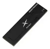
PCS.50A
Antenna, Chip, 1.71 GHz to 2.69 GHz, -2.6 dB, Linear, SMD
⚠️ Reference pricing provided. In case of supply shortages, we will connect you with our trusted procurement partners to ensure your project's continuity.
- Manufacturer: TAOGLAS
- Product type: Antennas - Single Band Chip
- SVHC: To Be Advised
- Product Range: Universe Series
| Delivery and price | |
|---|---|
| Units per pack | 250 |
| Price | 4.88 € |
| Current stock | 10+ |
| Lead time | 30 days |
Datasheet

+ ed yO iG Y) OO a| (© ' |1.|Introduction|3| |---|---|---| |2.|Operational Instructions of the PCSD.50.A|5| |3.|Specifications|7| |4.|Antenna Characteristics|9| |5.|Radiation Patterns|11| |6.|Mechanical Drawing|23| |7.|Antenna Integration Guide|24| |8.|Packaging|34| |9.|Application Note|35| |10. Solder Reflow|10. Solder Reflow|37| ||Changelog|38| Taoglas makes no warranties based on the accuracy or completeness of the contents of this document and reserves the right to make changes to specifications and product descriptions at any time without notice. Taoglas reserves all rights to this document and the information contained herein. Reproduction, use or disclosure to third parties without express permission is strictly prohibited. SPE-21-8-119-A www.taoglas.com 2 ## 1. Introduction The Taoglas Universe PCS.50A is a patent pending active Cellular and GNSS antenna designed specifically for IoT devices with small ground planes. With an unprecedented level of integration, it combines aperture tuning and active switching technologies to provide a wideband coverage for GNSS and most 4G cellular bands, including the most challenging 700MHz bands. The PCS.50 has an RF switch to adjust the resonance frequency of the antenna depending on the device requirements. The aperture tuning technology allows the antenna to cover the whole spectrum of 4G LTE bands by adjusting the resonant frequency of the antenna to the desired frequency band of operation. This allows the device to use the correct frequency band required by the radio module. Additionally, a second active switch can be simply added if either Cellular or GNSS needs to be selected. * The PCS.50A is compatible with the radio modules that support RF front end control interface (RFFE). The radio module controls the active RF switch to adjust the antenna resonance frequency to operate efficiently on multiple bands and increasing the RF capabilities by 3dB compared with standard passive solutions. This will in turn improve the Total Radiated Power (TRP) and Total Isotropic Sensitivity (TIS). The PCS.50A is easy to integrate using standard SMD technologies, and implementing the active solution is easy thanks to Taoglas’ integration support, providing different design files depending on your requirements. The antenna can be tuned by simply selecting the best switching the configuration to achieve the optimum antenna performance. Please see section 2 of this datasheet for the key operational instructions of this antenna to ensure optimum performance. Section 3, 4 and 5 of this datasheet shows the PCS.50A antenna performance on Taoglas evaluation board PCSD.50A. Section 7 shows how to integrate the antenna into your device and the Application Note in Section 9 demonstrates the products use in different scenarios. SPE-21-8-119-A www.taoglas.com 3 The PCS.50, tuned for PCBs to a size of just 40 x 50m, makes it suitable for even the smallest of IoT and CATM devices. Typical applications include IoT devices such as smart sensors requiring cellular and GNSS connectivity, wearables or asset tracking. The antenna itself measures just 38 x 10 x 1.6mm and as it is manufactured from high grade FR4 PCB, it is lightweight, yet robust and it is supplied on tape and reel. Contact your regional Taoglas customer support team for quick and professional support from our senior engineering team on integration and matching of the antenna to your device. *Depending on the capabilities of the radio module used. SPE-21-8-119-A www.taoglas.com 4 ## **2.** Operational Instructions of the PCSD.50.A Taoglas developed an evaluation board called PCSD.50.A that includes the PCS.50.A antenna, RF switches and other components to operate this smart antenna solution. This is available to order from Taoglas. Taoglas developed this EVB to help customers in implementing this solution on their application. The evaluation kit uses a simple RF switch SP8T to select different matching circuits and a SPDT to select GNSS or LTE radios. The RF switches used in the evaluation kit are: - SP8T: Infineon BGS18GA14E6327XTSA1 - SPDT: Infineon BGS12SN6E6327XTSA1 In the evaluation kit, both RF switches are controlled by the DIP switch, representing the control interface of the radio module. The DIP switch is connected to a 3V coin battery (CR02032). The DIP switch has two states: 1 represents ON, 0 represents OFF. The DIP switch is a 10 way switch, numbered 1 to 10. - Pins 1-4 are used to control the SP8T (U2): Pin 1 controls the power to SP8T, Pin 2 controls V3 on the RF switch, Pin 3 controls V2 on the RF switch, Pin 4 controls V1 on the RF switch. - Pins 9-10 are used to control the SPDT (U1): **==> picture [201 x 143] intentionally omitted <==** **----- Start of picture text -----**<br> PIN 1=VDD Pin 4=V1 Pin 3=V2 Pin2=V3 SP8T State<br>1 0 0 0 S1: M1-ANT<br>1 0 0 1 S2:M2-ANT<br>1 0 1 0 S3:M3-ANT<br> 1 0 1 1 S4:M4-ANT<br>PIN 10=VDD PIN 9=CTRL SPDT State<br>1 0 GNSS-ANT<br>1 1 LTE-ANT<br>**----- End of picture text -----**<br> Pin 9 is the control input for the SPDT, 0 = GNSS Antenna, 1 = LTE Antenna, Pin 10 controls the power to SPDT. - Pin 5, 6, 7, 8 are not connected and therefore not used. The pin definition and control table are shown in the tables above. SPE-21-8-119-A www.taoglas.com 5 ## **2.1** Antenna Active Tuning Circuit Below is the Schematic of the PCSD.50.A using SP8T and SPDT. For the current setup, only the first 4 states, State 1 to State 4 (S1-S4 ), of the SP8T are used. The other 4 states are reserved for future applications. Four sets of matching circuits are placed after the SP8T RX1-RX4. The antenna performance is tested and recorded when each of them are connected. SPE-21-8-119-A www.taoglas.com 6 ## **3.** Specifications **==> picture [40 x 42] intentionally omitted <==** |**Electrical**|**Electrical**|**Electrical**|**Electrical**|**Electrical**|**Electrical**|||| |---|---|---|---|---|---|---|---|---| |||||||||**Max Input**<br>**Power**| |||||**Average**|**Peak**||**Id**|| |**Band**|**Frequency (MHz)**|<br>**State**|**Efficiency**<br>**(%)**|<br>**Gain**|**Gain**|**Pliti**||| |||||||**oarzaon**|**mpeance**|| |||||**(dB)**|**(dBi)**|||| |||||||||| |||S1|12|-9.2|-4.8|Linear|50Ω|5W| |**5GNR/4G**||||||||| ||698~746|||||||| |Band 12,17,28,29,85||||||||| |||||||||| |||||||||| |||S2|19|-7.3|-2.5|||| |**5GNR/4G**||||||||| ||746~800|||||||| |Band 13,14,20,28||||||||| |||||||||| |||||||||| |||S3|17|-7.7|-3.0|||| |**5GNR/4G**||||||||| ||800~880|||||||| |Band 5,18,19,20,26,27||||||||| |||||||||| |||||||||| |||S4|24|-6.2|-1.1|||| |**5GNR/4G**||||||||| ||880~960|||||||| |Band 5,8,19,26||||||||| |||||||||| |||||||||| |**GNSS**||S4|37|-4.4|0.8|||| |GPS L1, GLONASS G1, BeiDou B1,|1559~1610|||||||| |Galileo E1||||||||| |||S1|56|-2.6|3.2|||| |**4G/3G**||||||||| ||1710~2690|||||||| |Band 1,2,3,4,9,23,25,35,39,66||||||||| |||||||||| |||||||||| ||||**Mechanical**|||||| |Antenna Dimensions|||38mm x 10mm x 1.6mm|||||| |Material|||FR4|||||| |Weight|||2.5g|||||| |Soldering Type|||SMD Reflow|||||| |**Environmental**||||||||| |Operation Temperature||-40°C ~ +85°C||||||| |Storage Temperature||-40°C ~ +85°C||||||| |Moisture Sensitivity Level||3||||||| Results are based on the Evaluation board of 40mm x 50mm with ground plane length of 37.5 mm. The antenna efficiency values meet operator requirement for USA markets for CATM1 cellular technology. *Results are shown using the optimum state of the antenna on the evaluation board. SPE-21-8-119-A www.taoglas.com 7 ||**5G/4G Bands**|**5G/4G Bands**|**5G/4G Bands**| |---|---|---|---| |Band Number|5GNR/FR1/LTE/LTE-Advanced/WCDMA/HSPA/HSPA+/TD-SCDMA||| ||**Uplink**|**Downlink**|**Covered**| |**1**|UL: 1920 to 1980|DL: 2110 to 2170|✓| |**2**|UL: 1850 to 1910|DL: 1930 to 1990|✓| |**3**|UL: 1710 to 1785|DL: 1805 to 1880|✓| |**4**|UL: 1710 to 1755|DL: 2110 to 2155|✓| |**5**|UL: 824 to 849|DL: 869 to 894|✓| |**7**|UL: 2500 to 2570|DL:2620 to 2690|✓| |**8**|UL: 880 to 915|DL: 925 to 960|✓| |**9**|UL: 1749.9 to 1784.9|DL: 1844.9 to 1879.9|✓| |**11**|UL: 1427.9 to 1447.9|DL: 1475.9 to 1495.9|| |**12**|UL: 699 to 716|DL: 729 to 746|✓| |**13**|UL: 777 to 787|DL: 746 to 756|✓| |**14**|UL: 788 to 798|DL: 758 to 768|✓| |**17**|UL: 704 to 716|DL: 734 to 746|✓| |**18**|UL: 815 to 830|DL: 860 to 875|✓| |**19**|UL: 830 to 845|DL: 875 to 890|✓| |**20**|UL: 832 to 862|DL: 791 to 821|✓| |**21**|UL: 1447.9 to 1462.9|DL: 1495.9 to 1510.9|| |**22**|UL: 3410 to 3490|DL: 3510 to 3590|| |**23**|UL:2000 to 2020|DL: 2180 to 2200|✓| |**24**|UL:1625.5 to 1660.5|DL: 1525 to 1559|✓| |**25**|UL: 1850 to 1915|DL: 1930 to 1995|✓| |**26**|UL: 814 to 849|DL: 859 to 894|✓| |**27**|UL: 807 to 824|DL: 852 to 869|✓| |**28**|UL: 703 to 748|DL: 758 to 803|✓| |**29**|UL: -|DL: 717 to 728|✓| |**30**|UL: 2305 to 2315|DL: 2350 to 2360|✓| |**31**|UL: 452.5 to 457.5|DL: 462.5 to 467.5|| |**32**|UL: -|DL: 1452 - 1496|✓| |**35**|1850|to 1910|✓| |**38**|2570|to 2620|✓| |**39**|1880|to 1920|✓| |**40**|2300|to 2400|✓| |**41**|2496|to 2690|✓| |**42**|3400|to 3600|| |**43**|3600|to 3800|| |**48**|3550|to 3700|| |**66**|UL: 1710-1780|DL: 2110-2200|✓| |**71**|617|to 698|| |**74/75/76**|1427|to 1518|| |**78**|3300|to 3800|| |**79**|4400|to 5000|| |**85**|698-716|728-746|✓| SPE-21-8-119-A www.taoglas.com 8 **==> picture [559 x 366] intentionally omitted <==** **----- Start of picture text -----**<br> 4. Antenna Characteristics<br>a<br> 4.1 Return Loss<br>|<br>0<br>-2<br>-4<br>-6<br>-8<br>-10<br>-12<br>-14<br>-16<br>-18<br>-20 yy<br>600 750 900 1050 1200 1350 1500 1650 1800 1950 2100 2250 2400 2550 2700 2850 3000<br>Frequency [MHz]<br>PCS.50A_S1 PCS.50A_S2 PCS.50A_S3 PCS.50A_S4<br>Return Loss [dB]<br>**----- End of picture text -----**<br> ## **4.2** Efficiency **==> picture [526 x 284] intentionally omitted <==** **----- Start of picture text -----**<br> 100<br>90<br>80<br>70<br>60<br>50<br>40<br>30<br>20<br>10<br>0<br>600 750 900 1050 1200 1350 1500 1650 1800 1950 2100 2250 2400 2550 2700 2850 3000<br>Frequency [MHz]<br>PCS.50A_S1 PCS.50A_S2 PCS.50A_S3 PCS.50A_S4<br>Efficiency [%]<br>**----- End of picture text -----**<br> SPE-21-8-119-A www.taoglas.com 9 ## **4.3** Peak Gain **==> picture [515 x 302] intentionally omitted <==** **----- Start of picture text -----**<br> 6<br>5<br>4<br>3<br>2<br>1<br>0<br>-1<br>-2<br>-3<br>-4<br>-5<br>-6<br>600 750 900 1050 1200 1350 1500 1650 1800 1950 2100 2250 2400 2550 2700 2850 3000<br>Frequency [MHz]<br>PCS.50A_S1 PCS.50A_S2 PCS.50A_S3 PCS.50A_S4<br>Gain [dBi]<br>**----- End of picture text -----**<br> ## **4.4** Average Gain **==> picture [521 x 294] intentionally omitted <==** **----- Start of picture text -----**<br> 0<br>-1<br>-2<br>-3<br>-4<br>-5<br>-6<br>-7<br>-8<br>-9<br>-10<br>-11<br>-12<br>600 750 900 1050 1200 1350 1500 1650 1800 1950 2100 2250 2400 2550 2700 2850 3000<br>Frequency [MHz]<br>PCS.50A_S1 PCS.50A_S2 PCS.50A_S3 PCS.50A_S4<br>Aver Gain [dB]<br>**----- End of picture text -----**<br> SPE-21-8-119-A www.taoglas.com 10 **5.** Radiation Patterns **4 5.1** Test Setup 1 Chamber Setup SPE-21-8-119-A www.taoglas.com 11 ## **5.2** 700MHz 3D and 2D Radiation Patterns ## XY Plane ## XZ Plane YZ Plane SPE-21-8-119-A www.taoglas.com 12 ## 800MHz ## XY Plane ## XZ Plane ## YZ Plane SPE-21-8-119-A www.taoglas.com 13 ## 850MHz ## XY Plane ## XZ Plane ## YZ Plane SPE-21-8-119-A www.taoglas.com 14 ## 900MHz ## XY Plane XZ Plane ## YZ Plane SPE-21-8-119-A www.taoglas.com 15 ## 1700MHz XY Plane XZ Plane YZ Plane SPE-21-8-119-A www.taoglas.com 16 ## 1800MHz ## XY Plane ## XZ Plane ## YZ Plane SPE-21-8-119-A www.taoglas.com 17 ## 1900MHz ## XY Plane ## XZ Plane YZ Plane SPE-21-8-119-A www.taoglas.com 18 ## 2100MHz ## XY Plane ## XZ Plane ## YZ Plane SPE-21-8-119-A www.taoglas.com 19 ## 2300MHz ## XY Plane ## XZ Plane YZ Plane SPE-21-8-119-A www.taoglas.com 20 ## 2600MHz ## XY Plane ## XZ Plane ## YZ Plane SPE-21-8-119-A www.taoglas.com 21 ## 2700MHz ## XY Plane ## XZ Plane YZ Plane SPE-21-8-119-A www.taoglas.com 22 ## **6.** Mechanical Drawing (Units: mm) SPE-21-8-119-A www.taoglas.com 23 ## **7.** Antenna Integration Guide SPE-21-8-119-A www.taoglas.com 24 ## **7.1** Schematic Symbol and Pin Definition of The circuit symbol for the antenna is shown below. The antenna has 5 pins with only two pins functional (Pin 1 and Pin 2). Pins 3, 4 and 5 are not connected and are only used for mechanical integration only. |**Pin**<br>~~|~~|**Description**<br>~~|~~| |---|---| |1|RF Feed| |2|Tuning| |3, 4, 5|Not Connected| Please note you can download the design files, 3D model and 2D drawings from the website here: https://www.taoglas.com/product/universe-pcs-50-designed-for-iot-devices/ SPE-21-8-119-A www.taoglas.com 25 **7.2** Antenna Integration Depending on the size of the PCB, the antenna should ideally be placed on the PCB’s shorter side, this will allow the antenna to take advantage of a longer ground plane. SPE-21-8-119-A www.taoglas.com 26 ## | **7.3** PCB Layout The footprint and clearance on the PCB must meet the antenna specification (section 6). Below shows the antenna footprint and clearance through ALL the layers of the PCB. Only the antenna pads and connections to RF Feed and TUNE are present within this clearance area (marked RED). The clearance area extends 1.6mm from the antenna mechanical pads to the ground area. This clearance area includes the bottom side and ALL internal layers of the PCB. SPE-21-8-119-A www.taoglas.com 27 **7.4** Evaluation Board Shown below are images of the evaluation PCB used to measure the antenna and generate the results shown in this document. SPE-21-8-119-A www.taoglas.com 28 ## **7.6** Evaluation PCB Ground Plane Length Shown below is the PCSD.50.A with solder mask removed to highlight the PCB ground plane length. SPE-21-8-119-A www.taoglas.com 29 ## **7.7** Antenna Matching Circuit (SP8T RF switch configuration) The matching components M1-M8 are placed after the SP8T RF switch. These are used to tune the antenna resonances. The values for these components are shown in the mapping table below. |GPIO_1=V1|GPIO_2=V2|GPIO_3=V3|SP8T State|Matching<br>Components|Frequency coverage| |---|---|---|---|---|---| |0|0|0|S1: M1-ANT|7.5nH,<br>L-07C7N5JV6S|700-750MHz| |0|0|1|S2:M2-ANT|5.1nH<br>L-07C5N1JV6S|750-800MHZ, 1700MHz-2700MHz| |0|1|0|S3:M3-ANT|2.7nH<br>L-07C2N7JV6S|800-880MHz| |0|1|1|S4:M4-ANT|0R|880-960MHz, GNSS| |1|0|0|S5:M5-ANT|N/F|Reserved for future application| |1|0|1|S6:M6-ANT|N/F|Reserved for future application| |1|1|0|S7:M7-ANT|N/F|Reserved for future application| |1|1|1|S8:M8-ANT|N/F|Reserved for future application| SPE-21-8-119-A www.taoglas.com 30 An additional matching circuit at the antenna feed side may be necessary for some applications to provide additional tuning options. Taoglas recommend incorporating extra component footprints, to form an ‘’L’’ or “Pi” matching network between the antenna feed and the radio module. On the PCSD.50.A evaluation board, an L network is reserved but it is not used as there is a zero Ω link fitted in this case. SPE-21-8-119-A www.taoglas.com 31 ## **7.8** PCS.50.A Footprint Below shows the antenna mounting footprint this displays recommended size and layout of the pads on the PCB. These pads are numbered to correspond with the pads on the antenna. SPE-21-8-119-A www.taoglas.com 32 ## **8. Packaging** SPE-21-8-119-A www.taoglas.com 33 SPE-21-8-119-A www.taoglas.com 34 **8.9** Application Note Packaging PCS.50.A is a smart antenna solution that works together with a radio module creating a whole RF system. When using the PCS.50.A antenna as part of a design, a suitable radio module will need to be selected that can control a tuneable antenna solution. Typically, there are two types of radio modules that operate with a tuneable antenna solution: - Radio module with GPIO interface - Radio module with MIPI interface Depending on the radio module selected the RF switch should also have the same interface. As an example, a radio module with a GPIO interface requires an RF switch with a GPIO interface. SPE-21-8-119-A www.taoglas.com 35 Taoglas offer integration services for this device please contact customer services or local sales for more support. A mapping table will be generated during the integration service. The mapping table links the matching circuits with the frequency bands and RF states (one example is shown below). The mapping table will be programmed within the interface of the radio module. When the radio module selects the frequency band, it uses the RF switch to select the best matching circuits for that frequency corresponding to the mapping table. ||||||| |---|---|---|---|---|---| |GPIO_1=V1|GPIO_2=V2|GPIO_3=V3|SP8T State|Matching Components|Frequency Coverage| |0|0|0|S1: M1-ANT|7.5nH, L-07C7N5JV6S|700-750MHz| ||||||| |0|0|1|S2:M2-ANT|5.1nH, L-07C5N1JV6S|750-800MHZ, 1700MHz-2700MHz| ||||||| |0|1|0|S3:M3-ANT|2.7nH, L-07C2N7JV6S|800-880MHz| ||||||| |0|1|1|S4:M4-ANT|0R|880-960MHz, GNSS| ||||||| |1|0|0|S5:M5-ANT|N/F|Reserved for future application| ||||||| |1|0|1|S6:M6-ANT|N/F|Reserved for future application| ||||||| |1|1|0|S7:M7-ANT|N/F|Reserved for future application| ||||||| |1|1|1|S8:M8-ANT|N/F|Reserved for future application| PCS.50A covers both LTE and GNSS. An SPDT is used to choose between LTE and GNSS, if the customer only requires LTE, the SPDT can be removed from the circuit. SPE-21-8-119-A www.taoglas.com 36 ## **8.10.** Solder Reflow Reccomendations Packaging The PCS.50.A can be assembled by following the recommended soldering temperatures are as follows: *Temperatures listed within a tolerance of +/- 10º C The PCS.50.A is not limited to the number of passes through the reflow process. Smaller components are typically mounted on the first pass, however, we do advise mounting the PCS.50.A when placing larger components on the board during subsequent reflows. SPE-21-8-119-A www.taoglas.com 37 Changelog for the datasheet **SPE-21-8-119 – PCS.50.A** ## **Revision: A (First Release)** Date: 2021-12-06 Changes: First Release Changes Made by: Gary West ## **Previous Revisions** **==> picture [495 x 480] intentionally omitted <==** SPE-21-8-119-A www.taoglas.com 38 www.taoglas.com © Taoglas www.taoglas.com SPE-21-8-119-A 39
Updated at April 22, 2026
About Novapart
Novapart is a B2B electronic component broker specialising in stock shortages and cost reduction. We source hard-to-find parts and identify compliant alternatives across a catalogue of 410,000+ components from 500+ manufacturers.
Learn more →Stock Shortage Specialist
When a component is unavailable, discontinued or has an unacceptable lead time, we tap into our network of vetted European and Asian distributors to source what you need — without compromising on quality or traceability.
Request a quote →Compliant Alternatives
We identify pin-to-pin, electrically equivalent substitutes that meet the same certifications (RoHS, AEC-Q100, REACH) as your original specification — validated against datasheets, not just part numbers. Often at a lower cost.
BOM Analysis service →